#fpga
1 messages · Page 2 of 1
 wise ingot
 stark trench
Lol
 silk verge
I remember when "jump" was known as "load program counter"
stark trench
That name is still relevant
wise ingot
At the risk of sounding ignorant to modern architectures, isn't this what JMP instructions actually do?
stark trench
It is
If you look at DungV, all I am doing is using the first byte of the intermediate to adjust the program counter to the next location to go to
DungV now can handle 255 instructions
Though I have space to do up to 1023 instructions
Maybe 2047 if I really pushed it
wise ingot
stark trench
Though I have space to do up to 1023 instructions
I mean, there's nothing preventing you from loading your PC in 2 cycles, like the 6502 (which had an 8-bit data, but a 16-bit address bus) did ;P
stark trench
True lol
wise ingot
(you can see that many of my opinions on CPU design come from the 6502. This is probably bad)
:P
stark trench
6502 was a great CPU
wise ingot
stark trench
6502 was a great CPU
It's actually still a thing!
https://wdc65xx.com/integrated-circuit
stark trench
The 8081 is also still very popular, especially in PLC
silk verge
I have a sneaking fondness for the 1802 and its futuristic register-rich, load and store architecture, which presages some of the development of RISC
I'm fond of the 6502, but having cut my teeth on the 6800, it does feel like the cheaper version (which, of course, it is: the 6800 was $300 and the 6502 was $25 at the time)
wise ingot
silk verge
I have a sneaking fondness for the 1802 and its futuristic register-rich, load a...
Apparently, wdc makes some interestingly anachronistic devboards for the 65c02
silk verge
The 65C02 is a nice update in several ways too
wise ingot
Yeah, first of all it's CMOS ;P
 frozen flower
Turns out I did extremely well in the course! All that's left to do now is tinker on an actual FPGA now! 😁
wise ingot
frozen flower
Turns out I did extremely well in the course! All that's left to do now is tink...
Congrats! :D
stark trench
frozen flower
Turns out I did extremely well in the course! All that's left to do now is tink...
Nice work! 🎉
wise ingot
@stark trench : https://github.com/olofk/serv you might find this interesting

GitHub
SERV - The SErial RISC-V CPU. Contribute to olofk/serv development by creating an account on GitHub.
stark trench
I’ve seen it, pretty neat
I’ve known of it for a bit, someone resurfaced it the other day when I was probing about the size of other CPU cores on lattice fpga 🙂
wise ingot
stark trench
I’ve known of it for a bit, someone resurfaced it the other day when I was probi...
There is also a neat project on the GF180 shuttle that has a few serv cores wired up in a proto-JTAG
It's sad that there will probably be no more openmpw shuttles in the predictable future
But, I guess it should have been expected, with the economy being what it is
 heavy arrow
stark trench
I’ve known of it for a bit, someone resurfaced it the other day when I was probi...
heavy arrow
stark trench
I’ve known of it for a bit, someone resurfaced it the other day when I was probi...
@wise ingot: posts bit-serial RISC-V CPU
@stark trench: I've known about it for a bit

stark trench
wise ingot
There is also a neat project on the GF180 shuttle that has a few serv cores wire...
Oh yeah I did see that. I was contemplating whether I wanted spi or jtag to program my CPU
wise ingot
||SPI, obviously. It doesn't come with a huge specification and a VHDL-derived description language that makes AXI blush :P||
stark trench
Lol
silk verge
Oh, I wonder if there's an HDL implementation of an MC14500 single-bit CPU...
Hmm, untested... http://www.brouhaha.com/~eric/retrocomputing/motorola/mc14500b/
wise ingot
silk verge
Oh, I wonder if there's an HDL implementation of an MC14500 single-bit CPU...
You could make one ☕
Possible project idea?
silk verge
That might be within my abilities, it's a fairly straightforward chip. I wonder if it would fit in a TinyFPGA BX.
wise ingot
I love how it has pins to signify it's doing a jmp, etc etc
silk verge
Hmm, Jameco has a GAL20V8. Goldmine has a PAL20R4, but I don't think that's sufficient.
wise ingot
Ah, so you're going for the challenge?
(I have no idea about anything GAL or PAL-related (please don't read any double entendres into this sentence lol), so I can't say anything there)
silk verge
I originally learned HDLs programming PAL/GAL chips back in the 1900s. It might be interesting to reduce the MC14500B into Boolean equations.
And then compile PALASM.FOR and run it
wise ingot
It's probably possible
....not so sure about being able to compile PALASM.FOR though, at least on modern systems :P
If you do it, you should keep a blog of the adventure, if you have the time and mental energy. I think it'd certainly make for an interesting read
silk verge
The Gnu ForTran compiler should be able to manage it, and I'd rather do that than fire up Wine and run the DOS version
wise ingot
Sometimes I feel the call of the void giving me an inexplicable hankering to learn fortran.....
After all, it's for FORmula TRANslation... It can't make any worse code than numpy.... Probably will be a lot better too, since it'll be compiled
silk verge
They taught us ForTran, Modula 2, Pascal, APL, and assembler in college
wise ingot
OTOH, good luck finding someone to work with who wants to read FORTRAN
silk verge
Although I already knew ForTran and assembler (and BASIC)
wise ingot
(I mean, I could use C, but, meh)
silk verge
 heavy arrow
silk verge
The Gnu ForTran compiler should be able to manage it, and I'd rather do that tha...
heavy arrow
silk verge
The Gnu ForTran compiler should be able to manage it, and I'd rather do that tha...
If it originally ran on DOS it's probably expecting x86 real mode.
wise ingot
I'd guess fortran would be high-level enough not to make any such assumptions?
winevdm might be able to if that's the case, yeah
silk verge
But you're right, ForTran is high level enough that isn't a consideration
Amusingly, the keypunches were modified to punch Fieldata cards for our Univac instead of standard Hollerith
heavy arrow
silk verge
But I'm guessing Wine can do it.
16-bit mode, i.e. no memory protection. You'd need a DOS emulator for that.
silk verge
What's fun is watching Wine on a 22MHz SparcStation running windows for workgroups 3.1.
wise ingot
Do you have many "retro" machines?
heavy arrow
... and somehow probably still running better than Windows 3.1.
silk verge
I have a handful of "retro" machines, a 6800 evaluation board, a KIM-1, an Atari 800, etc.
wise ingot
Which one's your favorite?
silk verge
The 6800 holds a special place in my heart because it's my first computer, and I learned all the basic concepts programming it. But my favourite is easily the Atari 800, with all its smart peripherals offloading tasks from the main CPU.
I saved my money for a year and a half to buy that thing.
wise ingot
Did you pick it for architectural, or price reasons?
silk verge
Architectural, I loved the design and capabilities.
wise ingot
now I'm curious...
silk verge
It was an expensive beast (I had a friend who worked at Math Box, who got me the employee discount, so it was $756, which was serious money in those days)
I was well and truly tired of loading programs from cassette (waiting 20 minutes only to find something went wrong got old really fast). The Atari (being an Atari) had cartridge based programs, so I could fire up Basic, Assembler, or a host of other programs basically instantly. The GTIA chip gave full color graphics, including sprites (full height instead of the little boxes the Commodore 64 could manage), player-missle graphics, collision detection, and even light pen support. The POKEY chip gave very capable sound generation and supported up to 4 joysticks (analog, digital, or both), which doubled as 4-bit I/O ports. And an expansion bus for an assortment of peripherals.
silk verge
It was pretty much the class of the field. People derided it as a "games machine", ignoring the fact that games were the most demanding applications available.
It did have its quirks. It did its math in BCD, giving high accuracy, but dismal speed (trig functions took an appreciable fraction of a second).
wise ingot
(still are, to a point. There's a reason many ppl seeking workstations go buy a gaming laptop or build a gaming pc, though they'll never game)
silk verge
I have a friend's cast-off gaming PC running FreeNAS in the basement.
wise ingot
[personally, I feel those gaming laptops with the giant power bricks kinda defeat the purpose of getting a laptop though :P]
wise ingot
silk verge
I have a friend's cast-off gaming PC running FreeNAS in the basement.
hopefully you've removed the battery! 😅
silk verge
I haven't even removed the (once) fancy GPU, which is doing nothing as there's not even a monitor connected.
I forgot about the battery, as I forgot how crappy PCs tend to be, having been spoiled by using server-class computers as home computers.
silk verge
Through my employer, I have access to plenty of high-end inference engines.
wise ingot
silk verge
Through my employer, I have access to plenty of high-end inference engines.
I mean, obviously, but I thought it'd be fun to see how far it could go
silk verge
There may be an ancient-enough version of Cuda (or whatever) to support it, I dunno
 west salmon
Question for you seasoned FPGA folks: Do you have a recommended workflow for designing to a spec?
In software engineering, my workflow usually goes something like this:
- Project Requirements Documentation (PRD) - Either a formal version from a product team or a "one-pager" that lays out testable requirements for the project.
- Design/Architecture - Design and architect the solution to the requirements. This could be high-level, detailed, or a combination, as makes sense.
- Implementation - I generally use a Test Driven Development loop (write positive test for desired functionality that fails, write code so that it passes, refactor, repeat until done).
I would think of a protocol spec document as somewhere between 1 and 2 - most protocol docs that I've read provide both testable requirements and the actual spec of the data packet (serial) and timing. But, I suppose, I'm looking for how digital circuit designers approach interpreting a spec, prioritizing functionality to implement, etc.
silk verge
In the past, I've been known to use an Interface Control Document (ICD), which was the touchstone between two different systems, and specified all the details they required to interoperate. The notion is that if both sides adhere to the ICD, they'll be able to talk to each other. In many cases, neither side existed yet, so in practice, I'd often build simulators (with lots of debug facilities) for both sides, and get the simulators talking (this was great for finding issues in the ICD as well). Then I'd make the simulators available to the groups implementing the project. If they could both work successfully with the simulators, they should ideally work when connected together. This worked better than you might expect, but does involve a fair amount of extra effort. The big payoff is when a running system breaks, you can split it apart and use the simulators again to figure out which side isn't following the rules (I've had a bunch of 3AM panic calls where I did exactly this).
 vale geyser
i do some retro gal programming. wincupl and galasm are both available and work pretty well. galasm runs in linux and is easier than wincupl. wincupl if you want to simulate. web search should find either.
silk verge
I didn't know about GALasm, thanks for the tip!
stark trench
For anyone US based, I have 5 IcyBlue feather available on Tindie 🙂 https://www.tindie.com/products/29279/

Tindie
A Lattice ICE5LP4K Based Feather With LEDs, LiPo Charging, and 22 GPIO For FPGA Fun!
wise ingot
Congrats! Nice!
 umbral seal
Just ordered one (though your site actually) along with a Cast-Away since I'm running out of KB2040s and I might be able to use the size and those castellated edges for a project. Now I'll have two FPGA boards in case I mess up one of them once I start tinkering. lol.
stark trench
umbral seal
Just ordered one (though your site actually) along with a Cast-Away since I'm ru...
🤓
 umbral seal
 stark trench
👀

@silk verge I’ve finally got around to testing the lattice featherwing you were interested in. Going to put it through the paces and see if I can program it from a feather m4 and others
wise ingot
stark trench
👀
What's the board's color? Brown? Is this a phenolic PCB? Are these even still in production?
wise ingot
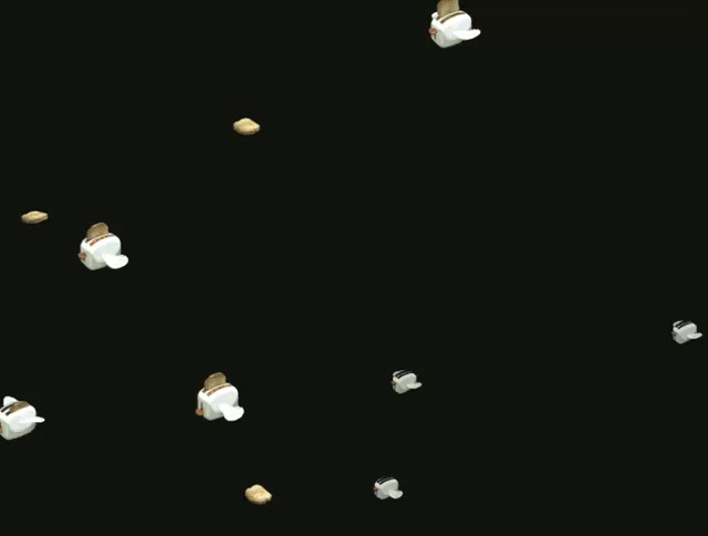
afterdark ;P
Jokes and potentially obscure references notwithstanding, it's a very interesting color. I guess it makes the traces easier to see?
(Therefore, it's easier to debug the board?)
wise ingot
What package is the IC? QFP?
stark trench
QFN
wise ingot
Hah, I saw tiny legs outside and assumed QFP 😅
OTOH that'd be too few IO for an FPGA
Speaking of, did you get lattice icecube2 to work?
stark trench
not yet, I spoke to a lattice FAE that works for arrow and they're going to investigate it
 lost spoke
wise ingot
https://tenor.com/view/toast-flying-toaster-gif-16812956
lost spoke
wise ingot
https://tenor.com/view/toast-flying-toaster-gif-16812956
great, now i have another thing to implement of my rpi, lol
wise ingot
Mr fancy over here has his personal FAE and offhandedly mentions it as if it's the most usual thing in the world 😅 (I'm just teasing you :P)
lost spoke
that at least sounds like a safer (copyright wise) way to demo sprites, vs just a mario running animation, and then running from nintendo's lawyers 😛
wise ingot
lost spoke
that at least sounds like a safer (copyright wise) way to demo sprites, vs just ...
FYI, the after dark flying toasters are copyrighted too. No idea who has the rights though
lost spoke
yeah, but that project has been "dead" for decades, and they arent nintendo
wise ingot
Sierra Entertainment was eventually acquired by Vivendi Games, which in turn was merged with Activision to form Activision Blizzard. The After Dark franchise will be owned by Microsoft pending international approval of their acquisition of Activision Blizzard.
lost spoke
nintendo does DMCA takedowns if you even play the game "wrong"
lost spoke
that could work, but is there a premade set of sprites for a running animation?
heavy arrow
lost spoke
nintendo does DMCA takedowns if you even play the game "wrong"
Yes, and they get away with it because nobody wants to get involved in a legal battle against them.
wise ingot
lost spoke
that could work, but is there a premade set of sprites for a running animation?
It's a platformer, so most probably yeah, if you're willing to spelunk the source code/assets?
lost spoke
sounds perfect
wise ingot

GitHub
SuperTux source code. Contribute to SuperTux/supertux development by creating an account on GitHub.
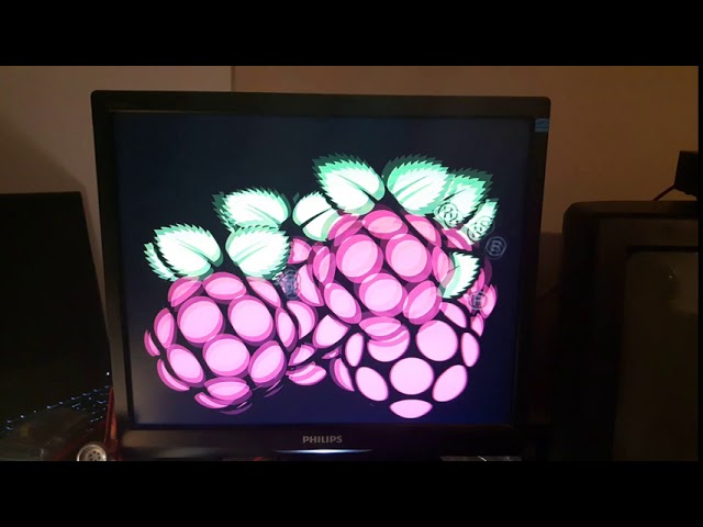 wise ingot
huh. Do you have a datasheet for the 2D accel?
lost spoke
the cpu was so low, it was exposing a bug in the cpu usage calculations, where it thought it was using negative cpu
wise ingot
I've been interested in playing w/. something like that for some time
lost spoke
lost spoke
the cpu was so low, it was exposing a bug in the cpu usage calculations, where i...
basically, there was a timer scheduled to check the cpu usage very 1000ms
it fired every 1010ms
and the program used 1ms over the last 1010ms, but the math assumed it was last 1000ms, and underflows happened
lost spoke
wise ingot
huh. Do you have a datasheet for the 2D accel?
i first found docs at https://blog.benjdoherty.com/2019/05/21/Exploring-Hardware-Compositing-With-the-Raspberry-Pi/
then wrote my own docs at https://github.com/librerpi/rpi-open-firmware/blob/master/docs/video-pipeline.md
and i have plenty of example code
wise ingot
Ah, so it's all reveng?
lost spoke
the linux source is well commented
lost spoke
originally, it was
with the legacy stack, dispmanx (the stack in the blob) managed everything
and the mailbox framebuffer would be used to map /dev/fb0 to a dispmanx sprite
or you can use the dispmanx userland libs, to create your own sprites
with the fkms drivers, linux exposes a DRM/kms api to userland, and then maps each DRM plane to a dispmanx sprite for you
then came the real kms drivers, where linux just takes over, and dispmanx is turned off
there is a chunk of display-list memory, uint32_t[4096] long on the pi0-pi3 model range
https://github.com/librerpi/lk-overlay/blob/master/platform/bcm28xx/hvs/hvs.c#L126-L149
void hvs_regen_noscale_noviewport_noalpha(hvs_layer *l) {
  assert(l->dlist_length == 7);
  assert(l->premade_dlist);
  uint32_t *d = l->premade_dlist;
  // CTL0
  d[0] = CONTROL_VALID
    | CONTROL_PIXEL_ORDER(HVS_PIXEL_ORDER_ABGR)
    | CONTROL_UNITY
    | CONTROL_FORMAT(gfx_to_hvs_pixel_format(l->fb->format))
    | CONTROL_WORDS(7);
  // POS0
  d[1] = POS0_X(l->x) | POS0_Y(l->y) | POS0_ALPHA(0xff);
  // POS2, input size
  d[2] = POS2_H(l->fb->height) | POS2_W(l->fb->width) | (l->alpha_mode << 30); // fixed alpha
  // POS3, context
  d[3] = 0xDEADBEEF;
  // PTR0
  d[4] = (uint32_t)l->fb->ptr | 0xc0000000;
  // context 0
  d[5] = 0xDEADBEEF;
  // pitch 0
  d[6] = l->fb->stride * l->fb->pixelsize;
}
you can then write 7 control words to it like this
repeat that, for each sprite
and then terminate it with a dlist_memory[display_slot++] = CONTROL_END;
then put the index for the start of the list, into a control register, and your done
wise ingot
wait, do they actually use the deadbeef magic, or is it just padding? lol
lost spoke
the 2d core will write to that slot on every scanline
it stores its own state in there
so its just padding, to reserve that space
wise ingot
Is that in DDR, or in some block SRAM inside the device?
(From the C, it looks like it's in DDR, but IDK how this platform compiles stuff :P)
heavy arrow
The OS doesn't really have control of what resides in memory vs. cache. That is handled by the hardware and possibly ucode.
lost spoke
there is a block of ram in the SoC, that is being used as 3 fifo's, but its basically just single-port ram, with 3 sets of r/w pointers
and those fifo's hold a stream of pixels for each active display
any time the fifo has room for 1 full scanline of image data, the HVS will parse the entire display list, and figure out what sprites are on the next scanline
heavy arrow
The OS can direct what regions of memory get copied into each FIFO.
lost spoke
it will then copy image data from dram->fifo
wise ingot
lost spoke
it will then copy image data from dram->fifo
Does REG32 tell the compiler that this maps to a hardware register?
lost spoke
that just casts an addr into a 32bit volatile pointer
and the * then de-refs the pointer
so gcc will read/write the addr
wise ingot
Ah. I haven't written any C code for ARM :)
lost spoke
this also isnt ARM
Yes, context memory (for display list) is embedded SRAM. It can do one pixel per cycle for palettised formats (compared to 4 pixels per cycle for unscaled, and 2 pixels per cycle scaled).
from one of the engineers
lost spoke
lost spoke
it will then copy image data from dram->fifo
so, for unscaled images, the HVS can copy 4 pixels per clock
for scaled images, 2 pixels per clock
and for palettised images, 1 pixel per clock
lost spoke
lost spoke
<https://github.com/librerpi/lk-overlay/blob/master/platform/bcm28xx/hvs/hvs.c#L...
CONTROL_UNITY tells the HVS that this image is to be rendered unscaled
CONTROL_FORMAT(gfx_to_hvs_pixel_format(l->fb->format)) is what pixel format the image data is in
enum hvs_pixel_format {
    /* 8bpp */
    HVS_PIXEL_FORMAT_RGB332 = 0,
    /* 16bpp */
    HVS_PIXEL_FORMAT_RGBA4444 = 1,
    HVS_PIXEL_FORMAT_RGB555 = 2,
    HVS_PIXEL_FORMAT_RGBA5551 = 3,
    HVS_PIXEL_FORMAT_RGB565 = 4,
    /* 24bpp */
    HVS_PIXEL_FORMAT_RGB888 = 5,
    HVS_PIXEL_FORMAT_RGBA6666 = 6,
    /* 32bpp */
    HVS_PIXEL_FORMAT_RGBA8888 = 7,

    HVS_PIXEL_FORMAT_YCBCR_YUV420_3PLANE = 8,
    HVS_PIXEL_FORMAT_YCBCR_YUV420_2PLANE = 9,
    HVS_PIXEL_FORMAT_YCBCR_YUV422_3PLANE = 10,
    HVS_PIXEL_FORMAT_YCBCR_YUV422_2PLANE = 11,
    HVS_PIXEL_FORMAT_H264 = 12,
    HVS_PIXEL_FORMAT_PALETTE = 13,
    HVS_PIXEL_FORMAT_YUV444_RGB = 14,
    HVS_PIXEL_FORMAT_AYUV444_RGB = 15,
    HVS_PIXEL_FORMAT_RGBA1010102 = 16,
    HVS_PIXEL_FORMAT_YCBCR_10BIT = 17,
};```image data in ram, can be in any of these formats
wise ingot
lost spoke
this also isnt ARM
I am going to sound completely stupid here, but, is there a different microcontroller inside the raspi SoC that you hit with that C code? If so, what arch is it?
heavy arrow
lost spoke
it will then copy image data from dram->fifo
Yeah, that'd mostly be handled by the DMA controller.
lost spoke
heavy arrow
Yeah, that'd mostly be handled by the DMA controller.
the HVS is a bus master, and can do its own DMA
lost spoke
wise ingot
I am going to sound completely stupid here, but, is there a different microcontr...
there are at least 5 turing complete cpu clusters within the SoC
the VPU is a dual-core RISC design, with a custom ISA
32 registers, 32bits each, some are special purpose like stack/pc/status, much like 32bit arm
and 64x64x8bit of vector registers
bootcode.bin, start(4).elf, recovery.bin and most of the example source ive linked, all run on the VPU
the VCE is somehow involved in mpeg2 license checks, and vc1/mpeg2/h264 encode/decode, and i suspect its turing complete
wise ingot
Ah yeah, I remember that; The VPU brings up the SoC
But I thought it was another ARM core
Since they already had the ARM license ;P
lost spoke
the ISP is involved in image scaling, pixel format conversion, and other camera stuff, but also helps out with h264 things
the VPU has been in the videocore, since before the arm 😛
originally, one of the ipod's ran on a videocore chip, entirely arm-less!
wise ingot
Ah, so videocore is past IP
lost spoke
and an engineer said, "why not throw an arm in, we might have a use later"
and thus, the bcm2835 was born!
wise ingot
 lost spoke
the V3D is the 3d core, which runs shaders
lost spoke
wise ingot
https://tenor.com/view/alive-itsalive-frankenstein-monster-gif-4795022
very much true
the bcm2711, is a vc4, with random vc6 things glued on the side
the vc6 design wasnt finished
so they just glued the new bits onto the old core
wise ingot
hah
lost spoke
so, the HVS, you give it up to 3 display lists, detailing every sprite on all 3 monitors
it will then top up 3 single-port FIFO's with scanlines, as room becomes available
the pixel valve, will read that single-port FIFO in a bursty fasion (with latency), and convert it into a proper dual-ported FIFO
the pixel valve then meters pixels out, at a configured pixel clock, while generating hsync/vsync/blanking signals, and turning the pixel flow off as needed
so now you have hsync/vsync/blanking, and 24bits of color
that is then routed to various encoders, hdmi/dsi/dpi/smi/vec
and turned into signals that can leave the SoC
wise ingot
How did we find all these out?
You'd typically need to sign at least one NDA to get this level of detail...
lost spoke
some of it from reading the linux source
some from just guessing or decompiling
and some from asking on the rpi forums
and engineers just say things
and some, from watching it malfunction when pushed to its limits
let me get an example...
  hvs_channels[2].dispbase = BASE_BASE(0)      | BASE_TOP(0x7f0);
  hvs_channels[1].dispbase = BASE_BASE(0xf10)  | BASE_TOP(0x50f0);
hvs_channels[0].dispbase = BASE_BASE(0x800) | BASE_TOP(0xf00);```these registers for example, define the bounds of the 3 FIFO's within the ram
linux will read them, to compute how big the fifo is, because it impacts vsync latency
but only start(4).elf will initialize them
wise ingot
Are you working on some sort of open FW for the pi?
lost spoke
yep

in this demo, i have too many sprites on screen
and if they all wind up on the same scanline, the HVS cant fill the fifo fast enough
and things begin to malfunction
the (s)nes is designed for a set resolution/pixel-clock, so they know the exact limits, and the hw forces sprites off when you do this
the rpi is too flexible, and they expect software to know the limits
wise ingot
is this the rpi1?
wise ingot
probably, since it's the only one that has composite I think
And it says "NTSC dance"
on the title
lost spoke
pi3 has composite
lost spoke
pi1+, pi2, pi3, and pi4, all have composite over the headphone jack
TRRS
original pi1 has headphone(TRS) + RCA
wise ingot
WAIT WHAT
lost spoke
pi0 has composite on a pair of 0.1" headers
wise ingot
o_o
lost spoke
the pi400 is the only model without composite
wise ingot
I thought the SoCs they used in >pi1 could not even output composite, hence the hdmi
OK!
lost spoke
whats more cursed, is that the bcm2835 has an FM radio in it
wise ingot
prolly disabled because of French DVB regulations?
lost spoke
receive only, and all of the required circuity is missing on every pi board
wise ingot
(Also, I've just realized we're having this discussion in #fpga , which is definitely not the right channel)
lost spoke
where shal we move?
lost spoke
doesnt really fit there
wise ingot
We need #digital-design-chat lol
wise ingot
I guess nobody uses it anyway 🙃
lost spoke
so, the HVS has a "current scanline" register
it then feeds pixels into the first fifo
the pv contains a second fifo, and fires the vsync/hsync irq
because of the depth of that 1st fifo, there is a lag to the vsync/hsync
and if the dram is slow to answer, that 1st fifo will run low, and the vsync/hsync lag changes

in this video, i setup the hsync irq
and then within hsync, i check if the "current scanline" is a multiple of something, like 5
if it is a multiple, i set the background color to blue, else white
wise ingot
ha
 wise ingot
You did the underclock to see what happens when there is high memory latency?
lost spoke
and then when it got to a zero-sprite region, it was able to generate a burst of scanlines, before the PV could hsync again
yeah
Yes, context memory (for display list) is embedded SRAM. It can do one pixel per cycle for palettised formats (compared to 4 pixels per cycle for unscaled, and 2 pixels per cycle scaled).
wise ingot
Fun fact: I've been wanting to play around with a SoC with built-in sprite management since I came across this datasheet https://www.generalplus.com/pLVfLN898SVpfSNnormal_download ; I had no idea the answer was in the raspi I have in my closet :P
Generalplus
凌通科技主要研發消費性的積體電路產品為主,擁有IC電路設計和應用軟體設計技術,包括Embedded Memory、類比IP和DSP等,以微控制器(MCU)為核心,衍生通訊、電玩/電腦週邊、遙控器、電子寵物等應用,同時擁有類比電路設計、嵌入式記憶體、液晶顯示、數位信號處理器及系統應用整合等技術,搭配重複再使用(Reuse)及系統整合單晶片(SoC)的設計能力,提供客戶最完善的整體解決方案。
lost spoke
and an engineer later let this slip, which answered everything
another 2 details...
this is actually very bad for performance
if you have 10 sprites covering the same pixel, you still have to pay to draw it 10 times
and due to the alpha, 9 of those draws go to waste
smaller sprites, with less overlap, means less waste, so you can have more sprites overall
a video game with proper collision between objects, would enforce that automatically
also, you need to draw to every pixel on the screen
if no sprite covers a pixel, this happens:

but, there is an optional background fill option, but that adds a flat cost, because it pre-fills every scanline
lost spoke
lost spoke
https://www.youtube.com/watch?v=EmSTdVAjv1E
this was using the bg fill, to quickly change the next scanline color
https://github.com/librerpi/rpi-open-firmware/blob/master/docs/pixelvalve.txt
            VC4           VC6
0x7e206000  pv0(DSI0/DPI) pv0(DSI0/DPI)
0x7e207000  pv1(DSI1/SMI) pv1(DSI1/SMI)
0x7e20a000                pv2(hdmi0)
0x7e216000                pv4(hdmi1)
0x7e807000  pv2(HDMI/VEC)
0x7ec12000 pv3(vec)```on the vc4 era (pi0-pi3), you have 3 hvs channels, and 3 pixel valves, and they are just hard-wired together
one pipeline can drive either dsi0 or dpi
one for dsi1 or smi
and one for hdmi or vec
smi isnt documented, dsi0 isnt brought out to headers on most models
so your only choice for pv0, is dpi
pv1, dsi1
and then pv2 has a choice, hdmi or vec
so you can run the pi1/pi2/pi3 in either dpi+dsi+hdmi, or dpi+dsi+vec, all tripple monitor!
the zero's dont expose dsi1 either

@wise ingot DPI is the simplest format, and you may have even generated it with a fpga before!
you could also easily make an fpga into a DPI capture card
ive also mis-configured DPI before, and wound up generating a 20,000 fps video signal
SMI is a multi-purpose bus, its able to access displays, generic chips, and NAND flash
SMI has a 18bit data bus, a 6 bit addr bus, and then some control signals
in one mode, it has a r/w direction, and a strobe to initiaite a transfer
in the other mode, its a read-strobe and write-strobe
in video mode, it just does bus writes, to a pre-configured 6bit addr, i think a FIFO in an external display
and you can mix in commands on the same bus
in theory, it can also access those old hitachi lcd drivers, fully hw accelerated (but not as a video port)
internally, vec can generate up to 3 analog outputs
in 3 output mode, it can do rgb and YPbPr
in 2 output mode, s-video
in 1 output mode, composite
but when putting the design onto the chip, broadcom only included 1 DAC
so its stuck with only composite
@heavy arrow can you see ways you might abuse SMI or DPI with a fpga?
heavy arrow
wise ingot
You'd typically need to sign at least one NDA to get this level of detail...
For basic display timings? That's publicly available.
lost spoke
heavy arrow
For basic display timings? That's publicly available.
but what about the whole chain from dram to video output?
heavy arrow
lost spoke
<@578805364019953715> can you see ways you might abuse SMI or DPI with a fpga?
You mean for general purpose high speed data transfer? You'd probably need to build a custom kernel module.
heavy arrow
lost spoke
but what about the whole chain from dram to video output?
Depends on the thing.
lost spoke
nope, can do it with the standard kernel
https://github.com/librerpi/rpi-tools/blob/master/smi-test.c
  int fd = open("/dev/smi", O_RDWR);
  ret = ioctl(fd, BCM2835_SMI_IOC_WRITE_SETTINGS, &settings);
    write(fd, buffer, count*2);
just load the right dtoverlay, set the bus timing params, and write your data!
when in 16bit mode, it will take every 16bit value from the buffer, present it on 16 pins, strobe a pin, then repeat
fully hw accelerated, including dma
wise ingot
heavy arrow
For basic display timings? That's publicly available.
(For the record, I wasn't referring to the basic display timings, but the internal architecture of the module)
[I may have accidentally forgotten to turn off the pinging in this message. Sorry!]
lost spoke
the vec can also malfunction in its own fun ways
it expects a pure 108mhz reference clock, which is used to derive the color burst
 heavy arrow
wise ingot
(For the record, I wasn't referring to the basic display timings, but the intern...
heavy arrow
wise ingot
(For the record, I wasn't referring to the basic display timings, but the intern...
It depends heavily on what it is and who makes it. AMD is one of the more transparent companies when it comes to video architectures.
lost spoke
if you give it even 108.1mhz, then a modern tv just goes "nope" and turns color decoding off

but an old tv doesnt care, and then drifts out of phase rapidly, because the signal is clocked wrong
wise ingot
heavy arrow
It depends heavily on what it is and who makes it. AMD is one of the more transp...
Yeah, I remember you linking that pdf :)
heavy arrow
NVIDIA and Broadcom are two of the most tight-lipped companies about it.
wise ingot
lost spoke
if you give it even 108.1mhz, then a modern tv just goes "nope" and turns color ...
Funnily enough, there was some discussion on this in the tiny tapeout server
lost spoke
heavy arrow
NVIDIA and Broadcom are two of the most tight-lipped companies about it.
and i have no idea how to drive the VEC in YPbPr/RGB/S-Video modes
the linux drivers lack support, because those dont work on any rpi hw
heavy arrow
I haven't really done anything with analog video, but I've worked quite a bit with DisplayPort.
wise ingot
heavy arrow
NVIDIA and Broadcom are two of the most tight-lipped companies about it.
Yeah, I figured as much :)
lost spoke
and those modes are only briefly mentioned in some headers broadcom released
i also havent been able to initialize hdmi or dsi from baremetal
those are far more complex to bringup, and PLLH wont lock
wise ingot
Isn't there relevant code in the kernel?
wise ingot
oh.
lost spoke
linux fails hard, because PLLH wont lock
linux can drive the entire video subsystem, once its been turned on
but the blob still has to turn it on
wise ingot
I assume PLLH is the PLL for the HDMI clock signal?
wise ingot
I'd recommend against that
Just spend the mental energy to make your own IP
And don't get yourself in a legal minefield
lost spoke
i think i'm just missing 1 power domain
and linux already has code to bring power domains online
i just have to point it to the right domain
so it doesnt seem like that big of a legal minefield
wise ingot
I am not a lawyer, but I assumed you meant decompiling/dissasembling the blob
lost spoke
i am doing that as well, to get hints
wise ingot
Oh. That's no good
lost spoke
for many hw blocks, thats the only option
wise ingot
Seriously, the trouble you could land yourself in is not worth it, though
lost spoke
the rpi engineers on the forum know i'm doing that, and havent said to stop
they get more upset if i decompile the usb3 controller firmware, lol
lost spoke
the first rpi engineers started out as broadcom employees
wise ingot
Oh well. I'm just saying (grumbles)
lost spoke
i think its more, that rpi/broadcom dont care what i do to rpi firmware
but they dont want to upset via-labs, where they buy the usb chips from
so they dont want me discussing that on the rpi forums
wise ingot
I'd recommend switching hobbies
lost spoke
oh, and that reminds me, many years ago, somebody bought a trial batch of bcm2835 chips from broadcom
they then promptly violated the license on the rpi formware, by running it on a non-rpi board
and broadcom has never sold to the public since
i think thats the extent of what they will do
wise ingot
Oh well, don't say I didn't warn you
lost spoke
as an example of how i can do things with just a hint...
this is linux code, for bringing a power domain up/down
complete with comments explaining every step
i dont know why its in a fork and was never merged, but it says SPDX-License-Identifier: GPL-2.0+ at the top of the file
#define PM_GNRIC                        0x00
#define PM_AUDIO                        0x04
#define PM_HDMI                0x58
and now you have a guessing game, which of these turns hdmi on?
i just need to try that, and see what happens
wise ingot
Do you have any other projects that don't involve peeking at other people's binaries? 😅
lost spoke
mostly haskell code, and stuff for nixos
ive also been porting zfs to little-kernel
and i can then run little-kernel on the VPU, as rpi firmware
so your /boot partition could be on zfs on the rpi
lost spoke
i use zfs on all of my systems
but LK did already have ext2 support, and i extended it to ext4
heavy arrow
There is no legal issue using zfs as a kernel module. It just can't be integrated into the Linux kernel itself.
Also linux doesn't have anything that can match zfs.
lost spoke
heavy arrow
There is no legal issue using zfs as a kernel module. It just can't be integrate...
and in my case, its more about, can i implement my own zfs driver, and link it into a kernel that is MIT based, with a bunch of GPL bits on the side
heavy arrow
GPL is the strictest part there, so if anything those GPL bits are going to give you trouble.
lost spoke
could i just label the whole thing as GPL?
heavy arrow
No. The entire reason zfs is not in the Linux kernel is because the license it was released under is incompatible with GPL.
lost spoke
but what if i'm writing my own zfs from scratch?
just reading a pdf that explains the on-disk structures
heavy arrow
Yeah you could do that probably.
lost spoke
then its not tainted by that license
 wise ingot
stark trench
wise ingot
stark trench
Nice! I presume you're sending the bitstream over (presumably) SPI?
stark trench
It’s the only way for ice40
wise ingot
You could even have the feather switch "personalities" mid execution
stark trench
SPI (host/peripheral)
wise ingot
Yeah
stark trench
I’ve got a few bugs to work out plus writing a tool to reverse bin files
You have to write the LSb first
I might also convert them to a text file
 mellow socket
stark trench
I’ve got a few bugs to work out plus writing a tool to reverse bin files
mellow socket
stark trench
I’ve got a few bugs to work out plus writing a tool to reverse bin files
inverting should be as easy as... (had to do a similar thing recently hehe)```py
def bitrev(bits):
"""Copied from some C code :P"""
bits = (bits & 0x0f) << 4 | (bits & 0xf0) >> 4;
bits = (bits & 0b00110011) << 2 | (bits & 0b11001100) >> 2;
bits = (bits & 0b01010101) << 1 | (bits & 0b10101010) >> 1;
return bits
loop that iterated the file
message = file.read(n)  # get next N bytes
message = bytearray(map(bitrev, message))  # beware your RAM usage
Assuming this is a Lsb first/last issue
Or like, you also have to start from the end? 🙃
stark trench
mellow socket
Assuming this is a Lsb first/last issue
Or like, you also have to start from th...
If I read the datasheet properly, it’s sending the LSb of the who thing first. I’ll have to experiment. I’m likely just going to make a tool that inverts the file and just send normally.
mellow socket
stark trench
If I read the datasheet properly, it’s sending the LSb of the who thing first. I...
Oh, so you have to invert the whole file and not each byte? How gross
stark trench
I need to see how iceprog is doing it and copy that
wise ingot
stark trench
If I read the datasheet properly, it’s sending the LSb of the who thing first. I...
oh, that's especially cursed 😅
wise ingot
mellow socket
stark trench
Btw, you were selling those, right? How bad is shipping to Spain? 👀
stark trench
mellow socket
Btw, you were selling those, right? How bad is shipping to Spain? 👀
Hard right now due to CE requirements
I’m trying to have that sorted by like the end of the year but we’ll see
After that, shipping should be ~$20-$30 because international shipping sucksss
wise ingot
stark trench
Hard right now due to CE requirements
Aren't there also exports regulations/compliance stuff (ensuring the end user isn't embargoed/is allowed to receive FPGAs etc etc)?
stark trench
wise ingot
Aren't there also exports regulations/compliance stuff (ensuring the end user is...
I mean, I’m kind of lumping compliance together
Not all fpga have export controls but it’s a matter of being thorough
wise ingot
stark trench
Not all fpga have export controls but it’s a matter of being thorough
I see! OTOH, the commercial software is very controlled
(no idea what the status of the OSS stuff is)
stark trench
wise ingot
(no idea what the status of the OSS stuff is)
Considering it’s on GitHub and accessible anywhere GitHub is, it’s probably difficult to enforce export controls if any on it.
Generally export controls relate mostly to specific IP types that can be built on the fpga. I’ve mostly seen it focused on wireless/wired communication protocols, anything remotely related to DoD.
But there are plenty of things, especially related to cryptography that are export controlled
wise ingot
stark trench
Generally export controls relate mostly to specific IP types that can be built o...
Possibly so. I am not American, and all I know is the form I have to fill out to be able to download vivado :)
wise ingot
stark trench
Considering it’s on GitHub and accessible anywhere GitHub is, it’s probably diff...
Tangent: I remember sourceforge (remember sourceforge? 😅 ) asking whether the project had "strong cryptography" in it on creation
stark trench
Lol
I work in an industry where export control knowledge is critical
So I am fairly familiar
Not an expert, but I am familiar
wise ingot
I can only imagine :)
Out of curiosity, if you can disclose, what makes an FPGA controlled?
wise ingot
Oh, that makes sense
wise ingot
@mellow socket See also past discussion starting from
#fpga message
stark trench
@wise ingot one area where my programming library is helpful is my upcoming RP2040+ice40 feather 🙂
I’m not sure if you remember sharing that
 wise ingot
stark trench
<@930143452749004830> one area where my programming library is helpful is my upc...
wise ingot
stark trench
<@930143452749004830> one area where my programming library is helpful is my upc...
I actually do!
You need to call it the mercury board. As a play on xilnx zynq (obviously joking :P)
stark trench
Lol
wise ingot
stark trench
Lol
I guess a fun application would be loading bitstreams according to the design's needs
* different bitstreams
stark trench
I actually should add a flag that checks total size of binary files to make sure they match platforms
Since bitstream files are always going to be specific sizes for each platform
wise ingot
stark trench
Since bitstream files are always going to be specific sizes for each platform
i mean, worst case, it'll just be rejected by the fpga, right?
stark trench
Probably
 viral ridge
stark trench
viral ridge
stark trench
Just asking, but why don't you use direct gnd connections for the gnd plane?
stark trench
viral ridge
Just asking, but why don't you use direct gnd connections for the gnd plane?
?
I use thermal relief so it’s easy to solder
viral ridge
Oh cool, yeah it's harder to hand solder with that. I mainly get my prototypes assembled elsewhere, and with a direct gnd with spokes noise and heat transfer makes it more reliable
wise ingot
TIL bluespec is open-source.
https://github.com/B-Lang-org/bsc
GitHub
Bluespec Compiler (BSC). Contribute to B-Lang-org/bsc development by creating an account on GitHub.
Think it'd be worth looking into at this point? ☕
wise ingot
EOS S3: MCU + eFPGA SoC with 100% Open Source Development Tools. Quickly get started in your next embedded design with EOS S3 complete open source platform
stark trench
wise ingot
<@728676724522352733> https://www.quicklogic.com/products/soc/eos-s3-microcontro...
These came out in 2020 I believe. I’ve never had a chance to try them out though
wise ingot
stark trench
These came out in 2020 I believe. I’ve never had a chance to try them out though
Yeah, they're not new, but I randomly came across them today and thought you'd find them interesting
(They're new to me xD)
stark trench
They’re technically new to me because I haven’t used them lol
wise ingot
you gotta make a devboard for them >:P
They're like ultra budget zynq with only 2k logic cells
(Or I gotta make one and send it to some PCBA to finally learn, if it doesn't require Too Many Layers)
stark trench
I think they have a qfn package
wise ingot
Looks like a devboard goes for ~EUR45
https://eu.mouser.com/ProductDetail/SparkFun/DEV-17273?qs=QNEnbhJQKvZWnZmS1ogf6w%3D%3D
Not great, not terrible
stark trench
Yeah
 vast moat
Nicely, there's also an EOS board available in the Feather form factor: https://www.crowdsupply.com/quicklogic/quickfeather
silk verge
wise ingot
They're like ultra budget zynq with only 2k logic cells
That seems really useful for a lot of projects.
wise ingot
silk verge
That seems really useful for a lot of projects.
Indeed!
stark trench
silk verge
That seems really useful for a lot of projects.
Just like an RP2040 with an FPGA :3

 glossy void
Wasn’t there a similar board that paired an fpga with an esp32?
stark trench
Ice-V
Esp32 + ice40
Also realizing one small mistake, I thought I broke out cdone, oh well. This is why we prototype lol
wise ingot
stark trench
They’re technically new to me because I haven’t used them lol
A strange quirk I noticed in this IC: They bridged AHB to Wishbone into the FPGA fabric
Possibly to avoid the AHB learning curve for the FPGA designer?
silk verge
I understood some of those words
heavy arrow
silk verge
I understood some of those words
"to"
(Actually I understand all of them)
wise ingot
silk verge
I understood some of those words
They are both protocols for point-to-point buses within SoCs/synthesizable designs in general.
AHB (AMBA High-performance Bus) is ARM's, used in things like the rp2040, and has strings attached to its use, while Wishbone is an OSHW thing.
heavy arrow
AHB is the midrange AMBA bus. There's also APB (low-speed) and AXI.
silk verge
So there's some middle ground between CPUs (like ARM) and FPGAs, and this is where these concepts live?
vast moat
silk verge
So there's some middle ground between CPUs (like ARM) and FPGAs, and this is whe...
Yes, these sorts of buses are how the ARM CPU core itself communicates with other things on the chip, like UARTs, timer peripherals, etc. and often the memory and flash too.
wise ingot
silk verge
So there's some middle ground between CPUs (like ARM) and FPGAs, and this is whe...
They also live within an FPGA design, for connecting modules with one another with a sort of standard interface
For example, if, in an FPGA design, you use an IP core provided by your FPGA vendor (or one you licensed from a company!), it will most probably use on of these buses for interfacing to the rest of the logic
silk verge
I remember the good old 6800 bus. And the weird old 1802 bus.
heavy arrow
It's memory mapped as well. You can think of it loosely as being analogous to PCIe, but instead of communicating with add-on cards it's communicating with different hardware blocks on-chip.
lost spoke
my rough understanding, is that the interconnect has N masters and N slaves
and typically, the addr range for each slave is hard-wired into it
something like the rp2040 has a 4 master to 10 slave interconnect, and can support all 4 masters accessing 4 unique slaves, on every clock cycle
but something like the bcm283{5,6,7}/2711, i think only supports one transfer at a time, but has FIFO's on the ports, to let things buffer up, and then burst over
wise ingot
lost spoke
my rough understanding, is that the interconnect has N masters and N slaves
and ...
that sounds about right, re: the interconnect doing address decoding.
However, there is no reason per se for an interconnect to be required; The connection can be a point-to-point one.
lost spoke
i can see how you would design the master/slave ports to be signal compatible
so you can just omit the interconnect for 1:1 links
and then its kinda like ethernet and a switch
you can either cat5 2 NIC's directly together
or you can cat5 3 NIC's to a switch
and functionally, there is no difference
wise ingot
lost spoke
i can see how you would design the master/slave ports to be signal compatible
That's how it works for most of these protocols. It's especially prominent when using AXI in FPGA designs, where you may want a part of your logic to interface to a specific IP core, and nothing more
(note that the most recent specifications use manager/subordinate)
lost spoke
wise ingot
(note that the most recent specifications use manager/subordinate)
the PC people have ruined SPI 😛
wise ingot
lost spoke
the PC people have ruined SPI 😛
For what it's worth, I don't think getting rid of historically problematic and awkward terminology is ruining anything. Like, there is no reason to reference actual slavery when referring to connection topologies!
Besides, it does not even make sense; A subordinate module can be the manager of a module that is downstream to it.
Anyway, I do not feel further discussion to this end would be productive.
lost spoke
more, that i cant make sense of the new SPI names
 edgy copper
Eh, the only annoyance I have on the SPI front is that with no actual standards body leading it
Different folk have settled on different naming conventions
lost spoke
and isnt philips and i2c making things worse in that area?
people are afraid of legal action, so they make up their own names, that are legally distinct, lol
so you wind up reading 2 paragraphs before you realize, "oh, its just i2c"
edgy copper
On the i2c front everyone tends to at least use the same terminology as phillips though
its still always scl and sda
wise ingot
edgy copper
Eh, the only annoyance I have on the SPI front is that with no actual standards ...
(FWIW, I am not really familiar with what's going on in the SPI front. I imagined they went for Manager/Subordinate like AXI did in AXI5)
edgy copper
With SPI, as there is no formal spec or governing body its been upto whomever makes a chip or board to label it as they please
lost spoke
from the rp2040 datasheet
 edgy copper
So I have seen at least two dominant replacement naming conventions, but also a few others
lost spoke
is txd relative to the manager or the subordinate?
mosi was very clear, txd is not
mosi can even still work with the PC correct naming!
manager out, subordinate in!!
edgy copper
The best replacement naming setup I have seen that is clear is simply swapping master for controller and slave for peripheral (and I have seen someone refer this way to an i2c bus too)
Though manager and subordinate I was just thinking the same thing as clever
lost spoke
oh, and the previous screenshot was a variant with rx/tx on the same pin
 edgy copper
Though of course problem with using controller/peripheral terminology to discuss a bus, is that you're using an on chip peripheral/controller
wise ingot
My guess is that the rp2040 licensed an SPI IP core, and took the signal names from its datasheet. The rest of the rp2040 datasheet uses the obsolete terminology
lost spoke
yeah, its using an IP core designed by arm
edgy copper
So now you're both referring to the actual silicon that provides the SPI interface as a controller, and its role as a controller
lost spoke
a random winbond spi flash chip
i would assume DO is out relative to the flash, so MISO
and DI is then MOSI

and now i'm remembering, some uart adapters, mis-label rx/tx, so a noob can just wire tx->tx, and rx->rx
because its too hard to teach them about cross-over!
and now you have to doubt the pinout of every uart adapter
wise ingot
edgy copper
So now you're both referring to the actual silicon that provides the SPI interfa...
IIRC the reasoning behind the controller peripheral terminology is recorded at https://www.sparkfun.com/spi_signal_names
PICO (peripheral in / controller out). For devices that can be either a controller or a peripheral; the signal on which the device sends output when acting as the controller, and receives input when acting as the peripheral.
POCI (peripheral out / controller in). For devices that can be either a controller or a peripheral; the signal on which the device receives input when acting as the controller, and sends output when acting as the peripheral.
edgy copper
Yeah I know and can follow its reasoning
wise ingot
(OK, sorry! :) )
edgy copper
Its just, now using the same term to describe 2 different things depending on context
If I just say SPI peripheral
am I talking contextually about something acting the peripheral role (or historically slave)
or am I referring to the MCUs SPI peripheral
manager/subordinate avoids that problem quite nicely
silk verge
I've been going with "host" and "target"
wise ingot
silk verge
I've been going with "host" and "target"
Not a bad choice; I typically use "Manager" and "Subordinate" when needing to work with things that have kept to the obsolete terminology, so that signal names that have M or S in them continue to make sense
"Typically used" (by me. As in, it's a personal practice. No idea how widespread it is)
EDIT: I rewrote the message so that it makes more sense
heavy arrow
wise ingot
Not a bad choice; I typically use "Manager" and "Subordinate" when needing to wo...
We use that at work, and to me it's almost worse.
wise ingot
heavy arrow
We use that at work, and to me it's almost worse.
TBH, I understand. Is there anything you would consider better in the context of, say, signal names within a module interfacing with a 3rd-party IP which uses the obsolete terminology?
(genuinely curious)
heavy arrow
Just use the acronyms.
wise ingot
How about in speech?
heavy arrow
Acronyms
In all honesty I prefer to use whatever terminology I think most accurately describes how the system operates. Master/slave is rarely if ever an accurate description.
And for the new SPI acronyms (POCI and PICO) I fully encourage use of 👉 and 🤏
I work with video SERDES chips, so I use source/sink, tx/rx, and ser/des a lot.
wise ingot
source/sink (or whatever else accurately describes your system and is not Whatever The Old Acronyms Stand For) is good
wise ingot
I've encountered it in audio contexts
heavy arrow
Yeah that too
wise ingot
I am also kind of growing fond of the convention of tagging the signals with the relevant module (something like input module1_ready, output reg module1_valid and so on)
heavy arrow
It works whenever you have point-to-point interfaces with a well-defined direction.
heavy arrow
wise ingot
I am also kind of growing fond of the convention of tagging the signals with the...
That kills reusability though.
That'd be appropriate for signal/wire names, but I wouldn't put references to another specific hardware block in the port definition.
wise ingot
That's fair. On the other hand, something like dma_axis_valid would be informative to the effect that you are expecting an AXI stream DMA to be connected there...
heavy arrow
I2C is where it gets messy. I have yet to find a good description since there is really no dedicated controller. If the clock and data lines are high literally anything can start talking.
And some devices do both, so calling them "controllers" really doesn't make any sense.
heavy arrow
Ah yes, politicize it. Brilliant!
wise ingot
heavy arrow
Ah yes, politicize it. Brilliant!
(For the record: https://en.wikipedia.org/wiki/Party_line_(telephony) )
A party line (multiparty line, shared service line, party wire) is a local loop telephone circuit that is shared by multiple telephone service subscribers.Party line systems were widely used to provide telephone service, starting with the first commercial switchboards in 1878. A majority of Bell System subscribers in the mid-20th century in the ...
[you most probably know this, but I am stating it for the benefit of anyone concerned about the server rules]
heavy arrow
Wasn't familiar with the term, but it makes sense.
west salmon
I'm still ideating and working on learning Vivado (and digital circuit design, overall). But, I'm wondering if you folks with FPGA and HW experience can give some guidance or thoughts on the right "primitives" to use for the use case that I'm working towards:
Effectively, a streaming video buffer, where multiple streams of pixel data can be written to asynchronously and arbitrary streams combined/composited to a unified output. For example, two virtual monitors' signals could be streamed to this "buffer" and the "mix" determined by some logic elsewhere that uses an IMU. Would a RAM buffer be the right choice for this? Or is there a better, less stateful, lower-latency construct that would be worth exploring?
If approaching this in software, I'd probably use something like a large array and select the output with pointers. But, I'd really like to solve it in HW/GW to both learn and potentially avoid the extra latency from running SW.
heavy arrow
You're describing an async FIFO, which can be implemented with the block RAM.
Or you can make one yourself.
west salmon
Thank you! That's exactly what I was looking for.
heavy arrow
This sounds like something DisplayPort related.
west salmon
Indeed! I'm looking to get to a DP implementation eventually. For the more immediate future, I'm going to abuse some cheap GPUs that can output DP.
heavy arrow
For video data you're going to need a pretty hefty FPGA, and you'll have to find a way to get the different video timings synchronized. Trying to composite a 1080p video on top of a 4k one in real time won't be particularly simple.
heavy arrow
west salmon
Indeed! I'm looking to get to a DP implementation eventually. For the more immed...
You're aware that MST allows you to transfer multiple streams over a single DP link, right?
heavy arrow
You'll want a bigger GPU, of course.
Also potentially useful:
http://www.sunburst-design.com/papers/CummingsSNUG2008Boston_CDC.pdf
west salmon
Indeed. And considering that I'm initially using a Zynq-7020 w/ 4.9Mb of BRAM, I'm probably going to need to use external memory in order to have a large enough "canvas", right?
heavy arrow
Probably.
west salmon
Thanks very much, again, for the guidance!
stark trench
The Lattice CrossLink-NX is an FPGA designed specifically for things like video and camera interfaces. It might be worth exploring their dev kit ($129)
wise ingot
stark trench
The Lattice CrossLink-NX is an FPGA designed specifically for things like video ...
(I don't think it has any onboard DDR out of the box though)
west salmon
Yeah. It looks like it might need help if wanting to use anything but DSI but, it has a ton of BRAM that can be configured as true dual port, which would probably work well for a streaming FIFO.
And I hadn't thought about that - was just thinking "will a PCIe Gen 2x1 be enough to pipe through a cheapo video card that can do 3840x1080?". A PI or PI-like SBC might work well.
west salmon
Hrm. Another couple of questions. I've found an RGB2DP IP offered for free by Digilent targeting the Zynq-7000 series. I've got an Arty Z7-20 (Zynq 7020) but there are not any multigig transceivers available, from my understanding though there are HDMI source and sink ports attached to the PL.
Could I potentially use the HDMI source port to transmit the DisplayPort data? If I understand the connector pinouts correctly, there are an equal number of data pins. Thinking about this, I'm suspecting that the HDMI source port might be too slow.
Alternatively, I have 49 digital I/Os in an Arduino shield form Factor. Could I potentially get enough bandwidth for a DP signal by splitting each lane into parallel in the fabric and recombining with a high-speed parallel to serial IC?
My goal isn't direct to display but to a USB PD Friend board to use the lanes for DP alt mode.
west salmon
I'll try to make it work anyway and see if Vivado shouts at me 🙂
wise ingot
west salmon
Hrm. Another couple of questions. I've found an RGB2DP IP offered for free by Di...
I think 7020 has serdes
west salmon
wise ingot
I think 7020 has serdes
Unfortunately, I don't think that that functionality came until the Ultrascale+ fabric. Fingers crossed that Avnet gets Zuboards back in stock.
 long bridge
why the heck is fpga software still so wack and clunky?
xilinx, intel
its just so frustrating to use
wise ingot
long bridge
why the heck is fpga software still so wack and clunky?
Which one are you currently using? Most have a TCL interface which allow you to mostly avoid their GUI
long bridge
vivado 2023. It does have a tcl interface
maybe one could just use vscode and the vivado tcl interface to compile? not sure how that'd work, and if its possible to add the the tcl tools to PATH so you could use it in another shell
oh seems like yo ucan, and theres apparently some usefu extensions
wise ingot
long bridge
maybe one could just use vscode and the vivado tcl interface to compile? not sur...
FYI, Although I've never used it, I've heard of https://github.com/olofk/edalize
 tribal badger
I just wish TCL wasn't such a bare bones interpreted language. It's so slow
 polar frost
 slate oak
my bad, you're talking the ui language
slate oak
my bad, you're talking the ui language
Really real programmers use bits driven by switches... or plug panels...
 molten hemlock
polar frost
Really real programmers use bits driven by switches... or plug panels...
molten hemlock
polar frost
Really real programmers use bits driven by switches... or plug panels...
😆 I've totally done that. Built a 6800 computer from scratch and programmed it using dip switches. But, yeah, I did a lot of wild things in the 80s.
polar frost
molten hemlock
😆 I've totally done that. Built a 6800 computer from scratch and programmed it ...
80s? What happened to the 70s? 🤓
molten hemlock
polar frost
80s? What happened to the 70s? 🤓
 silk verge
In the 1970s, I used a monitor (MIKBUG) to bit-bang a serial port on a 6800 to talk to an ancient Flexowriter teletype. In the 1980s, I had a graphical interface, keyboard, and light pen in the form of an Atari 800. In the 2000s, I used a hex keypad and 7 segment display to program a 6502 in a replica KIM-1. In the 2010s, I used toggle switches to control a simulated PDP-8. In the 2020s, I'm using a DIP switch to control a breadboarded 1802 and eyeing the notion of flipping bits in hand-woven core memory with a magnet on a stick.
long bridge
wow, all the way back in the 70s
silk verge
Yup. With my first computer (this one, which I still have). I no longer have the huge hulking Flexowriter, so now I use a much more powerful modern computer as a dumb terminal for it, via a custom cable I built to convert the TTL asynchronous serial port (which was originally implemented by replacing the intended RS-232 converter chips on the board with ordinary logic gates) via the 1/4" phone jack to USB.
 wise ingot
silk verge
Yup. With my first computer (this one, which I still have). I no longer have t...
wise ingot
silk verge
Yup. With my first computer (this one, which I still have). I no longer have t...
This paragraph reminded me of a period UNIX book I was reading one day; It described the terminal emulator as (and I'm paraphrasing here) "the program you use to turn your thousand-dollar computer into a hundred-dollar terminal"
silk verge
Yes, that's exactly what I'm doing. Making a 2GHz 64 bit computer with gigabytes of RAM pretend to be a terminal for a 1MHz 8-bit computer with 576B of RAM
silk verge
The CPU board is an ordinary Motorola 6800 evaluation board. My friend Fred built the enclosure, came up with the idea of using phone jacks as serial ports, then later, built a S-100 converter into it, to convert the Motorola bus into a more popular one, to support the commodity S-100 RAM boards behind it.
slate oak
It runs custom software
wise ingot
slate oak
It runs custom software
Given its nature, of course it runs custom software! My question pertains more to what kind of custom software it runs
:)
silk verge
It runs MIKBUG 🙂
wise ingot
Makes sense! A monitor suits these machines :)
 reef tusk
so hum... fpga can have thousands of logic units (so sensors(??)) like 100$ ones seems to have from 512 to 2056. But sensors uses a few tens/hundreds uA even just for logic signals. How does that compute together ? It would seem to be at some point you wont be able to power all of them / exchange ttl with all of them?
 plucky helm
Logic units aren’t sensors. More like tiny switches
heavy arrow
More like little blocks of SRAM plus some additional "glue logic".
reef tusk
but dont they get their input/logic from somewhere ands run some sort of logic gates on it ? So hundreds of them imply I'd need a source of 0 and 1 for their logic gates ?
sorry I kinda forgot the conversation the channel was muted
heavy arrow
reef tusk
but dont they get their input/logic from somewhere ands run some sort of logic g...
The "logic gates" are implemented in lookup tables (which are the small SRAM-like structures I was talking about). These logic blocks consume very little power when not switching. As far as power supplies are concerned, most FPGAs have multiple VDDIO supplies that control the logic levels for different I/O pin groups.
silk verge
And yes, FPGAs are (generally) digital, and operate on 1s and 0s.
 jovial zinc
any good resources so I can learn verilog? I have a clear goal in mind but have no idea how to get there
 mild agate
It's eons ago, but I learned from "Verilog HDL" by Samir Palnitkar. The language has evolved quite a bit since then, so I'd look for something more modern that is compliant with IEEE1364-2001.
mild agate
jovial zinc
any good resources so I can learn verilog? I have a clear goal in mind but have ...
Once you've found a text, you'll want a compiler and simulator to try things out. Icarus Verilog (https://steveicarus.github.io/iverilog/usage/index.html) can be used in combination with GTKWave to run some interestingly large designs.
heavy arrow
Personally, I recommend doing either VHDL or SystemVerilog. Regular Verilog tends to force some very bad habits.
Also, keep in mind that a lot of internet tutorials are not written from a digital hardware design perspective.
stark trench
heavy arrow
Personally, I recommend doing either VHDL or SystemVerilog. Regular Verilog tend...
I think the big bad habit of Verilog is that it’s pitched often as a “C like HDL” and then people (like me) end up getting frustrated when our designs don’t synthesize properly or at all because we designed it like another piece of software
VHDL at the very least forces you to think on a hardware level
heavy arrow
And that is why I prefer VHDL.
long bridge
take a look at chisel in scala
its quite good as an HDL that is close to verilog in some ways but incorporates higher level features
heavy arrow
Yep, it depends on what you want to accomplish though.
stark trench
I’ve been spending time getting better at prompt generation for ChatGPT. It’s a fun exercise, plus it’s a fun way to get ideas for fpga designs
Here’s the output Verilog for a random seed generator
module RandomSeedGenerator(
    input wire clk,          // Clock input
    input wire reset,        // Reset input
    input wire start_stop,   // Start/Stop control input
    input wire [2:0] frequency_selection, // Frequency selection input
    output reg [7:0] seed,   // Output seed
    output reg seed_ready    // Seed ready output
);

reg [7:0] lfsr = 8'd1;       // 8-bit linear-feedback shift register (LFSR)
reg [2:0] frequency_divider = 0; // Frequency divider based on selection

// Generate random seed based on LFSR
always @(posedge clk or posedge reset) begin
    if (reset) begin
        lfsr <= 8'd1;
        seed_ready <= 0;
    end else begin
        if (start_stop) begin
            if (frequency_divider == 0) begin
                // Update LFSR only when frequency divider is zero
                lfsr[0] <= lfsr[7] ^ lfsr[5] ^ lfsr[4] ^ lfsr[2];
                lfsr[7:1] <= lfsr[6:0];
            end

            // Output seed when ready
            if (frequency_divider == 0) begin
                seed <= lfsr;
                seed_ready <= 1;
            end else begin
                seed_ready <= 0;
            end

            // Decrement frequency divider
            if (frequency_divider > 0)
                frequency_divider <= frequency_divider - 1;
        end
    end
end
// Update frequency divider based on selection
always @(frequency_selection) begin
    case (frequency_selection)
        3'b000: frequency_divider <= 1000000; // Select frequency 1 Hz
        3'b001: frequency_divider <= 500000;  // Select frequency 2 Hz
        3'b010: frequency_divider <= 250000;  // Select frequency 4 Hz
        3'b011: frequency_divider <= 125000;  // Select frequency 8 Hz
        3'b100: frequency_divider <= 62500;   // Select frequency 16 Hz
        3'b101: frequency_divider <= 31250;   // Select frequency 32 Hz
        3'b110: frequency_divider <= 15625;   // Select frequency 64 Hz
        3'b111: frequency_divider <= 7813;    // Select frequency 128 Hz
        default: frequency_divider <= 1000000; // Default to frequency 1 Hz
    endcase
end

endmodule```I've put up a synthesizable example on github here: https://github.com/skerr92/ice5lp4k_examples/blob/master/RSG/top.v
stark trench
I am going to try and implement an AES encryption/decryption engine. Seems like a fun exercise
Thankfully the block diagram is pretty straightforward
 worldly oriole

This is our first video on implementing digital logic circuits in Verilog, a Hardware Description Language (HDL). In this lesson we'll go through the installation (Windows) for Icarus and GTKWave and write a very simple, hello world, style module and testbench.
 junior rapids
any good idea for a beginner fpga?
can i just buy any? if they are all programed with HDL does this mean they are "compatible" between each other?
stark trench
junior rapids
can i just buy any? if they are all programed with HDL does this mean they are "...
I’d recommend an iCE40 FPGA like icebreaker
Or even IceStick
junior rapids
stark trench
I’d recommend an iCE40 FPGA like icebreaker
ah yeah, ive heard of the ICE fpgas
ill see if i can get a good board in some months
i saw one named ICESugar i think? it came with a pack of PMOD's and it was like 35 dollars
stark trench
ICeSugar is also another one
There’s open source toolchain support for ice40 fpga, lots of examples
stark trench
I’m working on some updates for IcyBlue Feather

 eternal crown
I just picked up the TinyFPGA BX - ICE40. Any advice for a beginner?
silk verge
junior rapids
any good idea for a beginner fpga?
The Nandland Go board is another possibility, it happens to be the one I started with. It's supported by open source toolchains such as IceStorm/IceStudio/apio. https://nandland.com/the-go-board/

Introduction to the Nandland Go Board: The First FPGA development board you should buy. Purchase one here.
junior rapids
silk verge
The Nandland Go board is another possibility, it happens to be the one I started...
Oh that looks good, and yeah icestudio compatibility is pretty nice
 glad bough
Necroposting but you can also get ebaz4305 and other used fpgas. The first you can find it off AliExpress for like 25$, if you can source from china from places like goldfish they cost 5$
 onyx bobcat
Any suggestions for a good book/learning material on how HDLs are compiled into the actual routing+blocks on an fpga? (~ like the 'dragon book' but for fpgas?)
stark trench
onyx bobcat
Any suggestions for a good book/learning material on how HDLs are compiled into ...
I wouldn’t say compiled in the context of HDL, the word you’re looking for is synthesize, and then after that placing and routing (picking the best path through the fabric).
I’m not sure if there is a good book on how synthesis works, but let me look.
There’s a book called “Verilog HDL: A Guide to Digital Design and Synthesis”, it might be helpful

O’Reilly Online Learning
I personally ordered this book and it’s been a good reference for me: Verilog by Example: A Concise Introduction for FPGA Design https://a.co/d/aTbOwOO

A practical primer for the student and practicing engineer already familiar with the basics of digital design, the reference develops a working grasp of the verilog hardware description language step-by-step using easy-to-understand examples. Starting with a simple but workable design sample, inc...
mild agate
Another excellent learning resource for Verilog/SystemVerilog are the papers by Cliff Cummings, collected here: http://www.sunburst-design.com/papers/
Improve your Verilog, SystemVerilog, Verilog Synthesis design and verification skills with expert and advanced training from Cliff Cummings of Sunburst Design, Inc.
onyx bobcat
Thank you both for the suggestions!
stark trench
Hey folks, I’m taking a few preorders for the next revision of my IcyBlue FPGA Feather! USB C, hardware bugs fixed, and better layout for improved performance!
https://www.oakdev.tech/store/p25/PREORDER_-_IcyBlue_FPGA_V2.html#/
Oak Dev Tech
Oak Development Technologies or Oak Dev Tech is a hobby and DIY electronics maker specialized in modularized breakouts for rapid prototyping and hobbyist makers.


 stark trench
For anyone interested in just a featherwing to add on to your project, I’m taking orders for a Lattice FeatherWing: https://www.oakdev.tech/store/p23/Lattice-FeatherWing.html#/
Oak Dev Tech
How Chill! An icy edition to your feather wing collection brings a Lattice iCE5LP4K FPGA to your Feather'd shenanigans. Programmed over SPI, this FPGA feather wing brings every pin of the iCE5LP4K to 0.1" headers and the RGB open drain pins to a tiny yet bright RGB LED.

 stark trench
Hey @silk verge you mentioned a while back wanting to know when the FPGA feather wing I was working on would be ready, I’m getting boards and parts ordered today. Should be ready to ship in the next 2 weeks. 🤞
onyx bobcat
onyx bobcat
Thank you both for the suggestions!
For anyone in the future - additional resources I found scratched my itch:
https://www.coursera.org/learn/vlsi-cad-logic and https://www.coursera.org/learn/vlsi-cad-layout
and a list'o'links: https://www.reddit.com/r/FPGA/comments/10de0ow/resources_for_learning_logic_synthesis_and_place/
stark trench
For those wanting IcyBlue with the UP5K, I’ve added a preorder option to the IcyBlue product page: https://www.oakdev.tech/store/p25/IcyBlue_FPGA_V2.html#/
Oak Dev Tech
Oak Development Technologies or Oak Dev Tech is a hobby and DIY electronics maker specialized in modularized breakouts for rapid prototyping and hobbyist makers.


 stark trench
Just a heads up for anyone thinking about using IceCube2 from lattice semi. They’ve paywalled licensing at over $400 a year. It was once free and the only option for VHDL users. Thankfully Yosys won’t ever pay wall it with it being OSS.
stark trench
Lattice Feather Wing boards 🤓
 stark trench
Ordered the wrong 1.2V regulator 💀
Few more days till they’re (the fpga feather wing) ready to ship 😢
stark trench
They look good, just need the 1.2V regulator and they’ll be ready to test and package 🤓
 junior rapids
Thoughts on these cheap CPLD's that have been popping up on ali?
 silk verge
Probably fake chips, but might work. You'd need something to generate the bitstream, and something to program the chip (this can be tricky if the chips use a nonstandard algorithm). But could be handy if you want some random logic and 5V compatibility (I don't know of any 5V FPGAs)
heavy arrow
silk verge
Probably fake chips, but might work. You'd need something to generate the bitst...
The only ones I can think of that might be able to do 5V are the old microsemi ones.
silk verge
I was pleasantly surprised to find the 5V ARM CPU powering the Arduino R4. I have been toying with the idea of putting an FPGA and level shifters on a DIP carrier for 5V breadboard use.
heavy arrow
The tricky part is finding level translators that don't restrict use cases too much. I2C is a notable pain point there.
 versed sigil
increasing numbers of peripherals are 3.3V or lower, right? (though i wish 3.3V character LCD modules were easier to find)
stark trench
There are a large number of sensors too that are using 1.8V and lower as well
But usually those are newer sensors being fabbed on newer processes
heavy arrow
I believe the 5V requirement usually stems from the backlight. But even if the LCD driver requires 5V, you can still likely drive the data lines with 3.3V as long as you never read data back from the LCD (assuming VIH=2.4V).
versed sigil
what i've heard is that the larger LCDs (16 chars wide or more) can need a negative bias voltage for readable contrast if VCC is 3.3V
supposedly, lots of the 5V character modules have an unpopulated footprint for a charge pump controller to enable lower-voltage operation
i'm actually interested in experimenting with very low-power (primary battery, etc) projects, so actually running at lower voltages is useful. though i guess people like using EPD or other bistable displays for that?
silk verge
versed sigil
increasing numbers of peripherals are 3.3V or lower, right? (though i wish 3.3V ...
That's true, but I'm still breadboarding 50-year-old CPUs, and it occurred to me I could have a 3-chip computer using an 1802 for the CPU, an FRAM chip for both RAM and ROM, and a small CPLD/FPGA to implement the memory gating logic, a counter, a shift register, and a sequencer: combined with the 1802's DMA engine, that 3-chip computer could generate RS-170 video!
Then again, there's a nice supply of 1.8V RF430 CPUs with built-in NFC (they can even be powered by NFC) in discarded glucose monitors
versed sigil
silk verge
That's true, but I'm still breadboarding 50-year-old CPUs, and it occurred to me...
i remember using PAL/GAL chips for custom glue logic in school
silk verge
Yeah, I was a big fan of the GAL22V10
Used it in one project where a CPU (VMS320) booted in 8-bit mode, then shifted to 16 bits for operation. The GAL chip did the juggling of the memory address leads to make it all work (it also involved prescrambling the boot ROM to align with the interleaved addresses)
versed sigil
i'm remembering that Lattice (!) actually developed the GAL architecture (and that might have been how they got started?)
molten hemlock
Now I'm having flashbacks to when I worked for a PC clone company. The 486 had just come out and our senior engineer had designed a board to work with it. The thing was this enormous 4-layer board covered in PALs. Unsurprisingly, the first run of boards didn't work. Some design issues but a lot of production flaws. Dozens of trace shorts, mostly on internal layers. We eventually worked through them all but what a nightmare.
 wheat pewter
IceCube2 is very archaic software, surprised to hear they intend to charge for it
stark trench
It’s probably part of a push to EOL the fpga it supports but are not supported in Radiant. Push people to more cost effective parts
silk verge
At least PALASM is free (and open source, well early versions are).
stark trench
Indeed
silk verge
I wonder if I could replace a 74181 with a PROM. An FPGA could do it easily, but I think it's stateless and deterministic, so perhaps a PROM could do it. It would be goofy to build a PDP-11/05 using PROMs as the ALU...
stark trench
Would be cool to see if you could do it
Also, looking at recent lattice pre releases.. I think they want to axe all the lower model fpga because they’re not well suited for AI/ML and neural networks due to memory constraints
The lowest level that can is the UltraPlus lineup
silk verge
That's annoying, there aren't a lot of parts we can use with FOSS and the vendor-specific ones are ... awful.
stark trench
Yeah.. probably buy up lower level parts while we can
I don’t imagine them doing a slow wind down
silk verge
Altera was looking at going open source (in 2015) but then they were acquired by Intel, who naturally abandoned that.
There's a little support for some Xilinx parts in Symbiflow and F4PGA. And QuickLogic is still out there.
I'm also keeping an eye on Raptor
stark trench
Gowin is based on OSS tool chains
And then there is another one I can’t think of the name of..
Cologne Chip came out with an OSS buildable fpga
versed sigil
i want to look at how versatile the CCL feature of the new AVRs is. sounds like a subset of PAL/GAL capabilities and possibly runtime configurable?
heavy arrow
stark trench
Gowin is based on OSS tool chains

GOWRON mentioned?
Oh wait, GOWIN
Close enough.
heavy arrow
versed sigil
i want to look at how versatile the CCL feature of the new AVRs is. sounds like ...
Last I looked in a datasheet it was basically a single logic element. It has a lookup table, a few flip-flops, and some additional glue logic. That's about it.
stark trench
heavy arrow
Last I looked in a datasheet it was basically a single logic element. It has a l...
Better than nothing I guess lol
silk verge
Speaking of Gowron, we just took a batleth class with Robert O'Reilly and J. G. Hertzler
 stark trench
Lattice Responded to the outcry in the change of licensing structure and has now added a free option for hobbyist, education, and start ups
wheat pewter
Sounds like damage control...
stark trench
wheat pewter
Sounds like damage control...
It absolutely is.
stark trench
Okay, the PCBs arrive, they’ve been assembled, and they work! 🥳
Say hello to the Lattice FeatherWing!
 wheat pewter
I used ICE5LP4K before. Fun times
stark trench
wheat pewter
I used ICE5LP4K before. Fun times
It’s a great little fpga. Great for learning, doing some light DSP, blinking lights, and related 🙂
junior rapids

GitHub
Super Nintendo Entertainment System for Tang FPGA boards - nand2mario/snestang
Snes on tang 20k and tang 25k fpgas

 supple pulsar
It looks like a largest power-of-two detector, but you wrote a module that only detects exact powers of two
I found some relevant links:
https://hdlbits.01xz.net/wiki/Always_case2
http://www.catb.org/esr/faqs/smart-questions.html
 little dagger
as you can see m trying to create a sine wave
I'm trying to take advantage of quarter symmetry but this seems not a sin wave i can't seem to figure out the fix here

so will be helpful if anyone's got an insight
lost spoke
little dagger
as you can see m trying to create a sine wave
I'm trying to take advantage of q...
might be something to do with signed vs unsigned, and if its centered on 0 or int_max/2
if the DAC expects unsigned numbers, then 0 is the lowest voltage and INT_MAX is the highest voltage, and the sine must be centered on INT_MAX/2
little dagger
lost spoke
might be something to do with signed vs unsigned, and if its centered on 0 or in...
honestly the only problem m having is that 3rd quarter wave is starting after the next posedge
i can modify the pair quarter but the next pair starts after next posedge
lost spoke
to me, it looks like if you shift half of that waveform down, (by the length of the steep drop), it will line up and form a perfect sine
little dagger
lost spoke
to me, it looks like if you shift half of that waveform down, (by the length of ...
I'm loading the values from a ROM
lemme just share the code
lost spoke
but if the rom is loaded with signed values, that go from -128 to +127
and you feed them to a DAC that expects unsigned from 0 to 255
little dagger
nope no negative values
they are unsigned indeed
I'm doing 0 511 so 10 bits or 9
i can do 255 too

sin_rom_lut dut1(
                          .clk(clk),
                          .addr_rd(phase_accumulator[30] ?  ~phase_accumulator[29:21] : phase_accumulator[29:21]),
                          .data_out( sine_sym1)
                      );

//reg addr10_delay1; always @(posedge clk) addr10_delay1 <= phase_accumulator[31] ;
//reg addr10_delay2; always @(posedge clk) addr10_delay2 <= addr10_delay1;


reg [9:0] sine_sym2;

                      always @(negedge clk ) begin

                      sine_sym2 = phase_accumulator[31] ? {1'b1,sine_sym1} : {1'b0,-sine_sym1};  // second symmetry
                      sin_wave = sine_sym2[9:1];   end
@lost spoke what do you think
lost spoke
is {1'b0,-sine_sym1} going to try and do twos complement negative?
lost spoke
i assume your currently testing in sim?
can you also graph phase_accumulator and sine_sym2?
little dagger
lost spoke
i assume your currently testing in sim?
can you also graph `phase_accumulator` a...
 lost spoke
little dagger
~ - got me confusing
lost spoke
little dagger
~ - got me confusing
so the - i copied is going native? and i could see that causing these problems
little dagger
i can try replacing them with ~
lost spoke
having proper addition might also help
id need to see the raw numbers and think out the logic to see what the proper answer is
little dagger
hmhm
lost spoke
{1'b1, and {1'b0, is essentially switching between +(INT_MAX/2) and +0, so your having an offset
lets assume an 8bit space, just so i can work with the example numbers in my head
the high period of the waveform, would have a +128 offset, so the data spans from 128 to 255
and for the low periods, it would have a +0 offset, so it spans from 0-127

@little dagger and then looking at this, i can see that the sine doesnt span 0-127
it looks more like it spans 0-63?
lost spoke
as a simple idea, try discarding the MSB of sine_sym1
little dagger
it's synchronizing wrong
little dagger
lost spoke
as a simple idea, try discarding the MSB of `sine_sym1`
That I cant
I have to access the 512 sin values
9 bits
[8:0]
lost spoke
can you post the table of those?
little dagger
it's just this file
wait
im drunk
the individual values are 0-255
depth is 512
lost spoke
so it only has half the bit-depth you expected
lets see, the file starts at 0x100, and goes up to 0x1ff, then goes back down to 0x100, and keeps going down, to 0, then back up to 0xfc
that looks like a complete sine wave, centered on 0x100
little dagger
little dagger
 lost spoke
if phase acc bit 31 is low (the first half of the output, the low side) then it uses {1'b0,-sine_sym1}
my verilog is rusty, what does the - operator do to the values?
lost spoke
thats what i thought
so the 0x100 to 0x1ff slope, gets inverted, and becomes...
0xf00 to 0xe01 scope?
assuming it was 24bits
little dagger
odule phase_accumulator
#(
parameter N = 32, //phase_accumulator bits
//parameter OUTPUT_SIN = 9,
parameter FRW = 26
)
(
//INPUTS
input wire clk, //system_clock
input wire reset,
input wire [FRW-1:0] frequency_tuning_word,
//OUTPUTS
//output wire [8:0] sin_lookup_output,
output reg [N-1:0] phase_accumulator,
output reg [8:0] sin_wave,
output reg [9:0] sine_sym2
    );
    wire [9:0] sine_sym1;
//    wire [8:0] phase = phase_accumulator[29:20];


     always @(posedge clk or posedge reset)
     begin
      // FREQUENCY TUNING WORD M
        if (reset)
                begin phase_accumulator <= 0; end
                else
                begin phase_accumulator <= phase_accumulator + frequency_tuning_word; end
     end

      sin_rom_lut dut1(
                          .clk(clk),
                          .addr_rd(phase_accumulator[30] ? ~phase_accumulator[29:21] : phase_accumulator[29:21]),
                          .data_out(sine_sym1)
                      );

//reg addr10_delay1; always @(posedge clk) addr10_delay1 <= phase_accumulator[31] ;
//reg addr10_delay2; always @(posedge clk) addr10_delay2 <= addr10_delay1;


                      always @(posedge clk ) begin

                      sine_sym2 <= phase_accumulator[31] ? {1'b1,sine_sym1} : {1'b0,-sine_sym1};  // second symmetry
                      sin_wave <= sine_sym2[8:0];   end

endmodule
i should mention that if i use a the 512 values or 255 or whatever of a complete sin period
the graph comes good a nice sin wave of desired frequency
however
wouldnt it be absolute bonkers to use 1/4 of the memory to make that exact sine wave?
that
that's what im trying to do
lost spoke
little dagger
wouldnt it be absolute bonkers to use 1/4 of the memory to make that exact sine ...
yeah
for something like this, i would usually just open a spreadsheet and start bashing on it, until things look right
little dagger
can't say ive used spreadsheets like that
lost spoke
ive turned excel into an analog clock before 😛
little dagger
never knew it was possible
lost spoke
its easy!
first, extract the hour/minute/second from the current time
divide to get a percentage around a circle
convert from percentage to radians
sin/cos give you an XY coord for that angle
XY plot to draw a line from 0,0 to the desired angle
use 3 datasets with 2 datapoints each, to draw 3 lines, for the hour/minute/second hand
multiply the XY out of sin/cos to change the length of the hands
only problem, is that excel expects the spreadsheet to only be modified by a person, and doesnt re-compute when NOW() changes value
so you need to keep mashing the refresh hotkey
little dagger
lost spoke
so you need to keep mashing the refresh hotkey
or an auto clicker
little dagger
@lost spoke

phase_accumulator[31] delaying this bit worked
and i put all of it in single always block
lost spoke
nice
silk verge
That brings back memories
 supple pulsar
https://www.crowdsupply.com/signaloid/signaloid-c0-microsd
FPGA dev board in Micro SD form factor, iCE40UP5K with 128 Mbit flash
 silk verge
Like the Electric Imp board, cute
silk verge
little dagger
howd you implement it
Basically just a wide word divider, so instead of adding 1 to an 8-bit register, it adds large numbers (like 14751) to an 80-bit register.
Fortunately, in an FPGA, stuff like an 80-bit register is easy to implement
little dagger
mhmh
little dagger
silk verge
Basically just a wide word divider, so instead of adding 1 to an 8-bit register,...
did you improve it further then?
silk verge
It seems to work fine, now I'm working on the rest of it, like how to control it via SPI, and laying out a PCB to hold the FPGA, clock generator, DAC, power amplifiers, etc.
little dagger
thats what my job is rn actually
ic
im going to try using cordic algorithm too
thats why i was asking haha
silk verge
For the sine conversion itself, I'm just using a lookup table, as I don't need a lot of amplitude accuracy for this project, but I do need a lot of frequency accuracy
little dagger
frequency resolution?
silk verge
Both accuracy and resolution
silk verge
Basically I'm implementing very fine speed control of an AC motor
little dagger
but accuracy
i mean
if you're generating 1khz
it's just 1k freq of sin wave or
etc
silk verge
In this case, it will be near 60Hz, but needs to be precise, so I can set to 60.00001Hz for example
silk verge
Right. But it also needs to be accurate, which isn't hard, I can buy a 1.5ppm 25MHz oscillator off the shelf for $7 or so to drive the FPGA clock input
little dagger
mhmhm
junior rapids
I got one of dem fpgas
 silk verge
Oh, I'm not familiar with that one. I'm intrigued by the FPC connector (MIPI, maybe?) and the unpopulated SOIC-8 footprint (serial EPROM for fuse data?)
supple pulsar
Found some docs
https://dl.sipeed.com/shareURL/TANG/Nano/HDK
The display port almost looks like VGA in the schematic
Sipeed-中文下载站,资料下载.
mild agate
Intriguing indeed. Reading the schematic, the unpopulated SOIC-8 pads are for a PSRAM. Looking at AliExpress some versions ship with PSRAM installed. At <$10 a pop it's a bargain. It looks like development requires a Gowin tool for synthesis. Anyone out there tried one?
supple pulsar
I've tried the 9k a bit, it works but I don't know how high-end it is since I got an Altera board pretty soon after
silk verge
supple pulsar
Found some docs
https://dl.sipeed.com/shareURL/TANG/Nano/HDK
The display port al...
Looks like an LCD to me, signals like LCD_CLK, LCD_HSYNC, and a bunch of parallel RGB data. Resistive touch pad, too (but apparently just routed to test points).
 distant shell
The Gowin EDA software is not trash, the UI is pretty good but their synth and PnR tools are weird
It doesn't support certain VHDL features but I don't remember which one sorry.
And their IP generator is good but you can't edit an IP after it was generated, all of their IPs (even the FIFOs or BRAM) are encrypted you have to start all over each time you want to edit them
stark trench
I wanted to start the new years off right by having a starting point to continue my work making examples for the RP2040/ICE5LP4K feather I made this year. Made this super simple PWM over SPI example: https://github.com/Oak-Development-Technologies/rpga_pwm_spi
GitHub
A novel example of sending PWM values over a SPI like interface from the RP2040 to the iCE5LP4K on the RPGA Feather - Oak-Development-Technologies/rpga_pwm_spi
silk verge
Hmm, I had been wanting to learn how to implement an SPI target on an FPGA...
stark trench
This SPI example is more of a SPI like interface in that I have clock, enable, and a serial data pin. I set enable high to write 8 bits from a lookup table of sorts, then bring enable low for a clock cycle to push the new PWM value to the PWM logic
There’s a separate internal clock that drives the PWM logic
I possibly could change it to do 16 bit writes so I can select which color of the RGB led to change the PWM value on
silk verge
Mmmm dual clocks
My design (precision non-integral divider) will have several registers
stark trench
Definitely workable from the base I set up. For me, I tend to get hung up on the down the road details so if I can start small I can expand a little more easily with a good starting point to fall back to.
Updated that git repo with the 16 bit write example.
Kind of has a slow strobe effect with how I’m sending the PWM values
Changed the Verilog to set the registers that aren’t being set, to be 0. Makes a more clear display of changing the LED with the SPI stream
stark trench
Hey @silk verge here's an example for writing a bank of registers (256 8 bit register slots) https://github.com/Oak-Development-Technologies/ice40_spi_io_expander
GitHub
An IO Expander for ICE40 FPGA that interfaces over a SPI like interface. - Oak-Development-Technologies/ice40_spi_io_expander
silk verge
Oh, nice find, thanks!
stark trench
I wrote it this morning xD
it's not perfect and might need some help to work with actual SPI but it's close enough anyway lol
silk verge
The cool thing is I can try it and see (using some 3.3V MCU as a test host) and reflash until it does what I want
stark trench
My IcePython tool for circuitpython is quite handy to getting the bitstream loaded
silk verge
I've mostly been developing with apio
stark trench
APIO is pretty fun to use, IceStudio is fun as well thanks to being visually based
stark trench
hey @silk verge I further updated that register writing io expander example. Added the option for PWM output 🙂
Works pretty good too
silk verge
Cool, I'll have a look!
Looks like "enable" is more an address/data switch than a chip select?
stark trench
it's functioning as a chip select, I kind of view chip select as an enable pin on SPI
right wrong or otherwise lol
silk verge
Er, more like combined enable/latch, maybe?
stark trench
well, it gates the data input
if you're not sending it high (you could change it to be active low), it won't do anything with the data
though some weird nuance with it is right now I have to send clocks when enable is low to push in the new data to the actual registers
silk verge
Maybe I'm reading this wrong. It looks like you enable it, clock in 16 bits, then drop enable and send an additional clock which transfers the low 8 bits into the register indicated by the high 8 bits
stark trench
Since I'm using two clocks now, I might just let the HFOSC set the data when enable is low.
flow is:
enable high
send 16 bits (over 16 clock pulses)
enable low
(one clock cycle to set the data into register)
rinse repeat
while True:
    if (count == 16):
        count = 0
        flow_cnt = flow_cnt + 1
        if (flow_cnt == 11):
            flow_cnt = 0
        print("count reset", flow_cnt)
        pico16.value = False
        pico17.value = False
        #time.sleep(0.01)
        pico16.value = True
        #time.sleep(0.01)

    pico17.value = True
    if (pico16.value):
        pico16.value = False
    else:
        pico18.value = flow[flow_cnt][count]
        pico16.value = True
        print("doing some stuff, data: ", pico18.value)
        if (count < 16):
            count = count + 1

time.sleep(0.01)```pico16 is clock, pico18 is data, pico17 is enable
stark trench
silk verge
Maybe I'm reading this wrong. It looks like you enable it, clock in 16 bits, th...
I misread what you put here, yes that's what's happening currently.
it's not truly SPI, but SPI like at the moment
silk verge
Yeah, that's what I was guessing. If it's SPI like enough for my purposes, I'll go with it, as it's a lot more compact than the rigorously correct ones out there (which are hard to read as well)
stark trench
adding a secondary always block that just looks at posedge of the internal clock, you can move the data without additional clocks from the host
stark trench
I got it working without the additional clock to the FPGA using the HSOSC on a separate always block
That bit is pushed up along with new code
So, in theory you might be able to bitbangio the data now.
hehe it works
😄
stark trench
Alrighty, I pushed up some circuitpython code that works (bitbangio SPI)
stark trench
silk verge
Yeah, that's what I was guessing. If it's SPI like enough for my purposes, I'll...
Not sure if you saw, I got the example working with SPI 🙂
Pushed up with an example using bitbangio SPI
silk verge
Haven't had time to play with it, but following along
stark trench
No worries. I just wanted to make sure you saw it 🙂
stark trench
Today I learned that setting a pin on an ICE40 to high impedance means that if you are driving an LED from 3.3V to that pin, it won't turn on. I had the biggest brain fart and spent like 3 hours+ trying to figure out why the LED wasn't on when the pin was in high impedance mode.
I can hear my former EE professors collectively face palming at my realization hahaha...
stark trench
I tell ya, SPI reads are far more interesting to figure out that writing. I have it set up to read from my device, but there are some interesting bits coming across that are weird. They might be from not having a default value for registers at startup.
actually, I think it might just be a timing issue
wise ingot
stark trench
This SPI example is more of a SPI like interface in that I have clock, enable, a...
Why not sample the SPI clock/data in your (presumably much faster) internal clock domain to avoid having to deal with two of them?
stark trench
I could, yeah
wise ingot
(Also, I'm not sure the two clock domains are properly specified in the constraints file, though I don't know how the OSS toolchain works)
stark trench
wise ingot
(Also, I'm not sure the two clock domains are properly specified in the constrai...
SPI clock is simply driven from an external source so there isn’t much to specify. Internal clock is using the 48MHz HFOSC on the ice40
wise ingot
stark trench
SPI clock is simply driven from an external source so there isn’t much to specif...
Wouldn't you have to declare the clocks then constraint the path between the two domains?
stark trench
The clocks technically don’t cross
wise ingot
Then don't you have to set any detected paths as false for the timing analysis to hold?
stark trench
For the most part, it’s looking at separate logic values on specific internal paths. For setting data, a register functioning as a Boolean gates setting the value of the input register write along with monitoring the “enable/cs” pin
Similar is done for reads. The interesting part is incrementing register address based on the bit index being shifted out
stark trench
ICE40 FPGA never cease to amaze me. I set up some registers to be read in bits as they are sent so I didn't endian swap, and then I thought
"Wow, I have a ton of signals, lets make them multi-bit buses" and then I ran into where I wanted to use another register, but some values were getting overwritten, so I had to keep making the registers big enough so there wasn't any overrunning of other registers lol...
Anyway, latest and greatest is pushed up. Probably going to try and make some changes to the read over the course of this week to make it more consistent and maybe figure out using just one clock
silk verge
It's cool that if you have a use for something like an 80-bit register, you can have it
stark trench
I've not added to where you can do functions on the PWM. for now, it's coded inside the main toplevel verilog, but I'll change it to a separate module with the ability to select different function outputs. Ramp, Sine, Triangle, etc..
currently just doing the upward ramp and downward ramp on the RGB LEDs
wise ingot
silk verge
It's cool that if you have a use for something like an 80-bit register, you can ...
Ah yes, the blessing and curse of being in full control of the datapath :P
Speaking of trig functions, Ken Shirriff recently released this great article: https://www.righto.com/2025/01/pentium-floating-point-ROM.html

Intel released the powerful Pentium processor in 1993, establishing a long-running brand of high-performance processors. 1 The Pentium incl...
 twin aurora
Oh hey, theres a channel for this stuff!
Very little progress in the way of hardware since my boards still arent in but I finished figuring out the whole configuring workflow!
stark trench
twin aurora
Oh hey, theres a channel for this stuff!
Very little progress in the way of hard...
That’s pretty awesome! I went the easy route to program using circuitpython 😅
Wrote this little library here https://github.com/skerr92/Oakdevtech_CircuitPython_IcePython

GitHub
A library for programming iCE40 FPGA from Lattice Semi - skerr92/Oakdevtech_CircuitPython_IcePython
It’s fairly fixed at this time but I plan to eventually make it work for all ICE40 FPGA
It does CRAM programming though I could allow it to do flash writes as well
twin aurora
Oh man, awesome!
I dont really have any experience with circuit python or any hardware I know of that is supported by it unfortunately :]
Its nice to know at least other programmers exist. I was really surprised to not find any arduino or AVR program to write winbond flashes.
stark trench
twin aurora
Its nice to know at least other programmers exist. I was really surprised to not...
Adafruit has a SPI flash library I believe

GitHub
Arduino library for external (Q)SPI flash device. Contribute to adafruit/Adafruit_SPIFlash development by creating an account on GitHub.
supple pulsar
Currently thinking about making an FPGA dev board in the QT PY / XIAO form factor and running into how fat the RP2040 is
 stark trench
supple pulsar
Currently thinking about making an FPGA dev board in the QT PY / XIAO form facto...
stark trench
supple pulsar
Currently thinking about making an FPGA dev board in the QT PY / XIAO form facto...
Yeah, it’s a real challenge to fit anything meaningful in the QT PY form factor for FPGA. I have considered it for some of the small chip scale packaged lattice parts, or even the really small pin count QFN packages. The space for all the caps and power nets and flash make it a bit tricky. But CRAM is an option to save space on flash
 cursive token
supple pulsar
Currently thinking about making an FPGA dev board in the QT PY / XIAO form facto...
cursive token
supple pulsar
Currently thinking about making an FPGA dev board in the QT PY / XIAO form facto...
If you're looking for other somewhat standardized PCB form-factors, at around the same physical footprint, read the table of contents at https://github.com/joric/nrfmicro/wiki/Alternatives
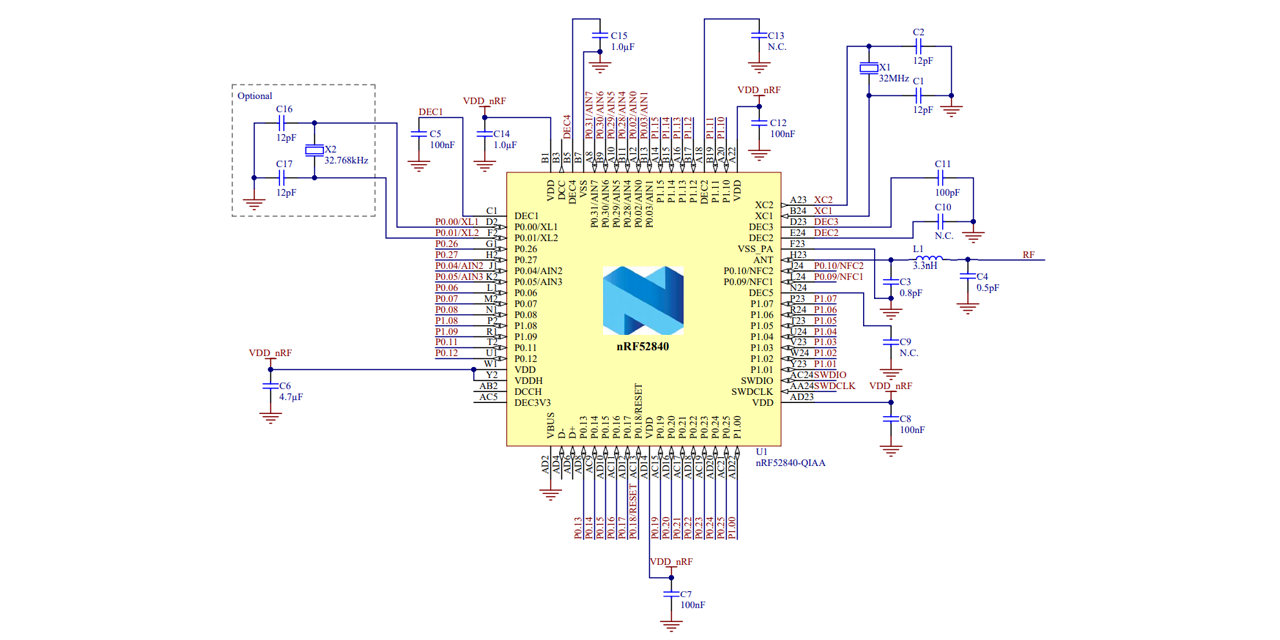
GitHub
A Pro Micro alternative for wireless keyboards. Contribute to joric/nrfmicro development by creating an account on GitHub.
 weak dune
I'm wondering if anyone has any time to share their experiences with Quartus. Im looking into it because my research has led me there.
I am considering the possibility of booting directly into the IME to eliminate the unused and insecure back end and utilize all resources provided.
It appears this may be possible with some FPGA magics...
Does anyone agree?
weak dune
Everything I've read says there is no shared FPGA fabric between the ARC processor and the user facing product but everything I do points to shared fabric. The microcontroller may be proprietary with signed firmware but it still appears to be an FPGA.
 raw carbon
stark trench
Yeah, it’s a real challenge to fit anything meaningful in the QT PY form factor ...
raw carbon
stark trench
Yeah, it’s a real challenge to fit anything meaningful in the QT PY form factor ...
I’m surprised they don’t stack the flash on top of the FPGA like the rp2358. But yeah, most FPGAs are ginormous
supple pulsar
That's probably much higher volume and a boutique memory chip, but I can't be sure. More package stacking would be cool and it will probably become more common in BGA applications if dies aren't stacked directly
supple pulsar
supple pulsar
Currently thinking about making an FPGA dev board in the QT PY / XIAO form facto...
Still working on it
 supple pulsar
Detour (Where on earth is an MCU going to fit?)

 soft spruce
Hi all, we're looking for feedback from embedded systems / maker gurus on our beta release of our IDE for our ELM11 / ELM11-Feather boards -> https://brisbanesilicon.com.au/elm11/elm11-ide/ ... feel free to reach out with any comments / suggestions etc
plucky helm
@north osprey I got the i2c interface after I resoldered a leg of one of the transistors
 wide dagger
Cool, a new channel
stark trench
Yay
silk verge
I stepped back from FPGAs for a couple of months, maybe it's time to get back in to it.
silk verge
I'm aiming more at the fast hardware functions myself. I just got some discouraging feedback on another Discord and lost all my motivation for a while.
stark trench
Behind every great creator is a group of naysayers. I’m eyeing up a Xilinx FPGA I used in my digital systems design class
It was fun to work with so I figured I’d get one to have fun with
vast moat
My "get one to have fun with" pick right now is the QuickFeather board using the EOS S3 chip... M4, DSP, and FPGA fabric in one. I've always been a fan of the combo of a MCU and an FPGA to do some really neat stuff.
stark trench
yeah, That's going to be a whole other Feather for me because I'm really loving the Lattice FPGA and I want to make a SoF (System on a Feather) to sell and work with
vast moat
Cool, yeah the Lattice parts are neat.