#help-with-hw-design
1 messages · Page 66 of 1
 knotty tiger
the reverse-biased capacitance has a dependence on the magnitude of reverse bias voltage, though this is rarely specified or characterized (except for things like varactors, which are diodes that are designed to act like voltage-controlled capacitors)
 verbal echo
ok, if I follow what @supple pollen said about AC, I think it'd hint to reading about diodes' behaviors in AC at different frequencies may help me understand the concept better. Is that a good next place to read?
knotty tiger
small-signal diode capacitance at reverse bias might be a mostly unrelated parameter to reverse recovery time, which you mentioned earlier. this is where the details of what you're trying to do are important
verbal echo
@knotty tiger I see, I spent days troubleshooting, and verifying the circuit that sparked this quest. And when my friend's solution was "I replaced the unknown-spec diodes with these..." I decided I wanted to understand what made it so.
Those specs are the first ones on the sheet I didn't understand.
knotty tiger
a forward-biased diode behaves (piecewise-linearly) like a small battery in series with a resistor. the voltage of the battery has a nonlinear dependence on the forward current, but this is close enough for small variations
verbal echo
I kinda made a small write-up about the issues I was seeing here: https://gist.github.com/slashfoo/2bdf703615d2279f3d7058f7bda4d34f and incorrectly assessed the problem to be code and opened this github issue https://github.com/adafruit/circuitpython/issues/6401 which has more details of what I was seeing and some attempts at schematics
knotty tiger
as you change from forward to reverse bias, that battery behaves a bit more like a capacitor charged to that forward "battery" voltage. that is what reverse recovery time tries to characterize (usually under specific narrow conditions)
verbal echo
knotty tiger
as you change from forward to reverse bias, that battery behaves a bit more like...
ok, a small battery in series with a resistor, where the battery's + is the diode -, and vice versa, or the other way around?
I mean the diode
let me edit
knotty tiger
no, the capacitor + is the battery's +. or if you like, the "forward-biased battery" is a capacitor charged to a "fixed" (actually dependent on forward current) voltage, that you can pretend is a battery until you change to reverse bias (or make a substantial change to the current)
verbal echo
Ok, hmmm, I still don't get it, forward biased means that the voltage at the anode of the diode is higher than the voltage at the cathode, right?
knotty tiger
ugh, this is almost easier to explain with a more detailed physical model involving charge carrier (electron and hole) distributions in the p-n junction. it's not "really" a capacitor; it's more accurate to say it's a physical distribution of charge carriers that acts kind of like a capacitor under some conditions. but i'm not up to explaining it in that amount of detail accurately
verbal echo
Let me provide a bit more color to my scenario
A summary of my observations is this: (screenshot is from the github issue I opened).
In that matrix Output pins (set low on setup) are D2, A3, D3, A2, D4, and A1; those are the
columns, and the input pins (pulled low on setup) are D5, A0, D6 and so on... those are the rows.
The way the matrix scan goes is this:
- Set the first column pin high.
- Read each of the rows and record which ones are high.
- Set the column pin low.


Repeat these steps for every column.
Everything works as expected when the matrix scan with an Atmega32u4 works, this is a 16MHz microcontroller, pin positions are the same but names differ.
The system misbehaves in the manners described there when running on an rp2040 (which runs at 125MHz), and solved by changing order of operations, adding delays, etc... or replacing the diodes as mentioned, which is how my friend solved this.
 knotty tiger
can you describe the timing details of when each pin is set to a given voltage or input/output state? because that's actually really important here
verbal echo
If I do this super fast, it appears as if I had closed more switches than the single one I did close; specifics and code are on those links.
timing details? I wish I knew those.
At setup I put the output pins to output, and set them to low. Then set the input pins to input, and set them to be pulled low with internal pull down resistors. Then I start the loop described above.
If I put sleeps to make the thing be slooooooow to the point I can see with my eyeballs and my multimeter, things behave properly.
knotty tiger
(hm, though if you're doing this in Python, you might not have an easy way to know without a logic analyzer, or maybe machine instruction level single stepping in a debugger)
what is the approximate resistance of the pulldown resistors? (they can tend to be large, which will make your problem worse, because t_RR is often specified at some substantial minimum reverse current)
verbal echo
I'd have to check what the pulldown values are on the atmega32u4 and rp2040 that I'm using, but I'd assume something like 10kOhm which is a value I see thrown at "pulldown/pullup mentions
knotty tiger
i'm finding a blurry screencap that seems to suggest 50kOhm to 80kOhm for the RP2040
are the output pins the columns or the rows in your diagram?
verbal echo
knotty tiger
what is the approximate resistance of the pulldown resistors? (they can tend to ...
does this mean that the reverse recovery may be affected by how little current the pull-down resistor is allowing to flow from the cathode of the diode to ground?
knotty tiger
you might be dealing with forward recovery time, depending on the timing of your signals, which i'm trying to piece together from your descriptions so far
verbal echo
Columns are the output pins, and Rows are inputs
I missed the part where I said that ─>| is a diode, ─/─ is a switch
verbal echo
knotty tiger
you might be dealing with forward recovery time, depending on the timing of your...
forward recovery time; I don't know what it is.
Is it the time that the diode allows the flow of current, or restricts it, when what conditions are met?
From the name I'm assuming it'd be the time it takes to go from not allowing to allowing flow of current when the voltage goes higher on the anode side than on the cathode side by whatever the threshold is for the diode.
knotty tiger
verbal echo
forward recovery time; I don't know what it is.
Is it the time that the diode a...
i think it's how long the diode takes to go from reverse biased to forward conduction, once the anode is at a higher voltage than the cathode
verbal echo
by more than the Vf (forward voltage)?
knotty tiger
V_f isn't a threshold; it's more like a point on an exponential I-V curve with an arbitrarily specified forward I_f
likewise, t_fr is specified at some specific voltage and/or current and starting from some specific reverse bias voltage
verbal echo
hmmm, so you think the problem I'm seeing is with the characteristic of the diode describing how fast they start allowing flow of current after I set the pin high. did I get that right?
as opposed to the capacitance spec that I also don't understand and asked about originally?
knotty tiger
yeah, and depending on what exactly the "resting" condition of the diodes in your matrix are, different parameters on the datasheet come into play
verbal echo
ok, I'm not sure if to keep trying to understand the two I was hunting after, or go after a new one... I know I'm a bit over my head on this, but I'm not really satisfied letting the mystery go unsolved past "I got these diodes and it worked", and want to start somewhere
knotty tiger
is your "resting state" all column lines output low, all row lines input with pulldown?
verbal echo
correct
knotty tiger
and keys that are pressed are reading as not pressed, i.e., reading low when you expect them to read high?
verbal echo
I mean, it's easy to understand what could have happened: the kit you got, had diodes with lower specs that worked for the atmega and the slowed-down code in the rp2040; and with the proper/known spec diodes things work.
But I don't have the spec or part number of the initial diodes, only that they don't behave well at the higher freq.
verbal echo
knotty tiger
and keys that are pressed are reading as not pressed, i.e., reading low when you...
no, the observations are that the key I pressed is properly registered, but non-pressed switches on the next row same column are registering as high/pressed as well, and in some versions of the code, sometimes two, or three.
knotty tiger
verbal echo
no, the observations are that the key I pressed is properly registered, but non-...
that is not something i would expect, given the circuit as drawn, unless there is some capacitive coupling in the board layout (which might actually be an issue, depending on the speeds we're talking about and the quality of the board design)
verbal echo
heh, exactly; so I thought that instead of trying to understand what's wrong with the circuit, I'd try to approach it the other way and try to understand what each aspect of a diode means, and how those behaviors change with frequency changes, perhaps I'll find a clue there
It seems like a fool's errand to be hung up on this question, rather than moving on after replacing the diodes. I thought the same thing when I saw the schematic of the board, which is exactly what I had constructed from the continuity tester of my multimeter while checking that there were no unexpected connections, and that all the diodes were soldered the right way
 supple pollen
verbal echo
I mean, it's easy to understand what could have happened: the kit you got, had d...
supple pollen
verbal echo
I mean, it's easy to understand what could have happened: the kit you got, had d...
I think you said they were 1N400X diodes, which are low frequency high current rectifying diodes: they both take a long time to switch between on/off, as well has have a large junction area and therefore a large capacitance.
verbal echo
anyways, thanks for at least taking a look and taking a stab at helping me understand some of it, I'll try doing more homework on textbooks and such (this is not for school, or work, just my hobby, but textbooks are a comfortable format for me)
verbal echo
supple pollen
I think you said they were 1N400X diodes, which are low frequency high current r...
when I mentioned the 1N40-something-something was when talking about the simulator, I don't know what diodes I got that didn't work at high speeds, I only know the part number/specs of the ones that solve the problem
which now that I'm on the computer again and not on my phone I can actually link to... this is the simulator I was trying to use to see where things break down or not https://www.falstad.com/circuit/
but the graphs for higher speeds aren't very useful as the scope just shows a solid chunk, but that's where you can select from different diodes.
I set a clock to go zero-to-5v square wave (rather than from negativeX to positiveX), 50% duty cycle (so goes half of the time off, half on, for whatever frequency is how I understand it), then poking different parameters for as simple of a circuit as I was able to make... Clock -> diode -> current limiting resistor -> GND
supple pollen
That matrix you depict probably has a fair amount of distributed capacitance as well, which will tend to slow things down. I'm unclear on how you're driving it, but if you're using the pull-up resistors for driving, that will also slow things down. Getting the best speed might entail some sequencing to directly discharge the distributed capacitances before switching to sensing mode to read the switch behavior.
However it seems like you're on the right track, using fast signal diodes instead of slow rectifier diodes.
knotty tiger
it occurs to me that at higher speeds (100s of MHz?), the open-circuit capacitance of the key switches might start to play a role. once you switch the column lines to high, you have to wait to charge up all the various capacitances attached to it, including parasitics, before you get a "true" reading from your switches. and if your inputs are pulled down with 50kOhm or so, that will slow things down more
supple pollen
Theoretically, but I'm unaware of any applications scanning keyboards at anywhere near that kind of frequency. You'd have all sorts of problem with capacitive/inductive/radiative cross-coupling at those frequencies as well, and might have to start looking at controlled impedance traces, matched terminations, etc.
verbal echo
I think I follow some of that, so it's not specs from the diode only that I need to take a magnifying glass to, but also my key switches and signal lines may be behaving in weird ways due to physical properties; i.e. open switches behaving as capacitors and so on
supple pollen
I really doubt you'll be running at high enough frequencies for those effects to be a problem.
Realistically, it's more likely to get problems caused by capacitive coupling of adjacent wires than the comparatively small amount across individual switches.
knotty tiger
i'm thinking of it in terms of time domain behavior, and what if you switch the column line high and read the row line before all the capacitances have charged up? i think you might very briefly get false high readings from open switches that way
supple pollen
Normally you'd be driving the columns from a fairly low-impedance source which should charge everything plenty fast (unless you elected to drive the columns with the pull-up resistors). The other (row) end of things might have some transient effects, that's what I was alluding to earlier when I mentioned pre-charging things on that end with active drive before reading. However, I doubt that complexity would be likely to be needed. You could always add lower-impedance termination to the row signals for faster performance and greater noise immunity.
verbal echo
the way they are driven is by digital writing 1, I think that's different from setting it to pull up, but I'm not sure
I never thought of using pull-up on an output pin
supple pollen
It depends on the pin mode. In the old-style Arduino model, if you set the pins to inputs and then write a high to them, it'll activate the pull-up. But if you set them to outputs, writing a high level to them will actively drive them high.
Normally there's no point using a pull-up on an output pin.
knotty tiger
supple pollen
It depends on the pin mode. In the old-style Arduino model, if you set the pins...
i think the RP2040 defaults to pull up or down, and no hi-Z on digital inputs?
supple pollen
But I personally have had some issues where I had a pin mode set wrong, and was inadvertently using the pull-ups instead of active drive because I had set the pin mode wrong.
verbal echo
the code I used actively set the columns as output and digital write zero to them, then set the rows as inputs and do pull-down
on setup that is
knotty tiger
even if the column line is driven high at low impedance, i think the charging current is limited by the high impedance pulldown plus other board leakages?
supple pollen
knotty tiger
i think the RP2040 defaults to pull up or down, and no hi-Z on digital inputs?
It looks like you can have pull-up, pull-down, or high-Z.
 supple pollen
knotty tiger
even if the column line is driven high at low impedance, i think the charging cu...
supple pollen
knotty tiger
even if the column line is driven high at low impedance, i think the charging cu...
Yes, that's why I mentioned the possibility of adding outboard lower-impedance pull-downs (1kΩ or so would probably work nicely)
verbal echo
ah, that sounds like a design consideration I should have in the design of my own board, which is a separate project to understanding this board which a friend designed
knotty tiger
some numbers for comparison: 1N4148 has c_d=4pF max at v_R=0V and 1MHz; 1N4001 c_d=15pF typ at v_R=4V and 1MHz, which is a substantial difference (and possibly even larger at 0V, looking at some charts)
verbal echo
I'm just stubborn on this one problem, it just doesn't stop itching... and I feel like it will keep itching if I solve the problem without understanding how the solution worked
@knotty tiger that's the capacitance value I was asking about, right? I think I remember those figures
supple pollen
Right: capacitance is proportional to the area of the plates (equivalent to the diode junction sizes) and inversely proportional to the distance between the plates (in a diode, this is essentially the thickness of the depletion layer, which is in turn dependent on the voltage: lower voltages are a thinner depletion layer and thus more capacitance)
This is, in fact, how varactor diodes work
knotty tiger
an RC time constant of 15pF * 50kOhm is about 0.75 microseconds? which is a substantial number of clock cycles at 100MHz
verbal echo
I went with the assumption that the incognito diodes are "some random common and cheap diode" and landed on the spec sheet for 1N40xx
supple pollen
Yeah, the 1N400X diodes are ubiquitous. For rectifying 60Hz power, they're dandy. As signal diodes, they're not great performers.
knotty tiger
so by my rough (and rusty) calculations, delaying 1 or 2 microseconds after driving the column line high might be enough to help some?
verbal echo
that guess wasn't too bad then, heh
supple pollen
That's probably what I would try first: it's easy and may well work. Doing fancy precharge logic is a pain (and carries a risk of a short circuit if something goes wrong), and adding 1kΩ pull-down resistors to the row signals involves procuring parts, soldering them, etc.
verbal echo
@knotty tiger I did a slowdown of 50ms and it worked, I believe I went down to 0.1ms and it reduced the effect considerably but not completely.
but at 125MHz of the rp2040, I'd be surprised if the matrix loop runs at 12MHz since I bet the loop in python is not THAT efficient to be only 10instructions
supple pollen
Even in C, I doubt it would be that fast.
verbal echo
but I feel like I'm getting distracted by details again; you have helped me in opening my eyes to other things that may also be influencing the scenario I'm observing, that I also don't understand. Which is helpful in its own right.
Thank you. I'm going to try to keep digging on my own, that way I stop burning your generously provided time
knotty tiger
verbal echo
<@824013908490059826> I did a slowdown of 50ms and it worked, I believe I went d...
that's a considerably longer delay than i would think would be necessary. it's hard to guess more of what's going on without logic analyzers and/or oscilloscopes
verbal echo
I got a logic analyzer within my budget, but I read that I want to capture at speeds at least 2x of what I want to observe, so I didn't even bother hooking it up because it's not that fast, and I don't have an oscilloscope. I may be able to secure time using one, but that's far in the calendar for unrelated reasons
supple pollen
An ancient 5MHz analog student oscilloscope would be sufficient.
verbal echo
noted, thanks again for the guidance @supple pollen and @knotty tiger
 glacial gale
whats the latency of a system bus nowadays. On a desktop motherboard or mobile board
supple pollen
glacial gale
whats the latency of a system bus nowadays. On a desktop motherboard or mobile b...
It's a little hard to characterize, due to things like multi-level caching
glacial gale
it seems like it is mostly irrelevant and throughput and bandwith is a bigger thing
glacial gale
supple pollen
It's a little hard to characterize, due to things like multi-level caching
true
supple pollen
It depends on what you're doing. Latency affects some things, and bandwidth affects others. Even some systems from years ago (Sun's XBus and Apple's G5 bus) can handily outrun most of the stuff built today in some ways.
glacial gale
for a general purpose laptop or phone, would bandwidth be the bigger thing? Since you want to make it responsive to the users actions, which is pretty slow
supple pollen
In my experience, software has more of an effect on responsiveness than hardware. Even a pretty modest system can seem quite zippy (as you correctly pointed out, humans just aren't that fast compared to computers). Bandwidth will tend to impact data heavy actions (for example, searching for a string or cryptography), whereas latency will tend to impact heavily random-access actions (for example, some kinds of equation solving and simulations).
One hidden slowdown is task switching: most computers these days are running multiple things, and switching between them a lot can slow everything down if the switching takes a long time. This is one of the reasons the aforementioned Sun systems seemed so fast even with fairly slow CPU clocks and dozens of simultaneous users: they had special CPU support that let them task switch in a single instruction.
glacial gale
supple pollen
One hidden slowdown is task switching: most computers these days are running mu...
im interested in that special instruction. Do you know if it saved variables to the stack or maybe ran all the software in kernel space?
supple pollen
It actually had multiple copies of all the CPU registers on-chip, so the instruction would just swap out the registers, one set for each process.
In those days, an X86 chip would save off all the registers into memory, taking over 1300 clocks to do so.
glacial gale
wow, that def sounds like it would have some big impacts when you have many threads waiting in each cpu queue
supple pollen
You've got it.
 normal star
I don't know if it is the best place to ask this question.
I was looking at a schematic of a device that is broken and I found a short in the a capacitor. When I look at the schematic it seems that this is suppose to be the case because there is a diode that allows the flow to go from the positive side of the capacitor to gnd.
I can't imagine that is right so can someone explain it to me?
 supple pollen
Those are funky symbols, at first I thought they might be diacs. It does look like one of the diodes would conduct if there's voltage on the capacitor, but that schematic looks odd, I'm not sure it's correct.
normal star
Yeah I also doubt it. I looked up the part and it is a switching diode with two diodes in opposite direction
but thanks! I thought I was going crazy
Hmm it is weird, overnight the short dissapeared in the circuit
I think the schematic is wrong like you said
 inner rampart
I made a new version of my feather spi adapter board, now with Battery pads and EN pads

 rigid raft
so I'm using an old CPU that's rated for operation at 5V. I have 10nF decoupling capacitors at all the pertinent power pins, quite close. I decided to measure the voltage across them, and when I turn the power switch off, I get a short burst (100ns max, ~100 to 200 MHz) of ripple. some of these peaks will reach up to 6V. here's a waveform

Should this be a cause for concern for longevity of the part?
I've been testing this part for a while now, and I've done many many power cycles on it, and it has survived, and the high frequency and short duration (and only occurring during power-down) leads me to believe it's fine, but I'm not super well-versed on what CPUs can handle.
I also don't know if it's my setup that's introducing some noise. I have lots of wires going everywhere (this measurement is off of a PCB, but I have 2x ~2 inch wires to connect to the decoupling cap terminals)
 inland jungle
usual recommendation is at least 0.1uF for decoupling caps, no?
rigid raft
I was using a reference schematic, which used 0.01uF, but I can easily swap them

putting in a 0.1uF might increase the amplitude of the 100MHz signals
 distant raven
rigid raft
putting in a 0.1uF might increase the amplitude of the 100MHz signals
distant raven
rigid raft
putting in a 0.1uF might increase the amplitude of the 100MHz signals
Usually there’s some mix of 1uF,0.1uF, and 0.01uF caps
Some analysis I’ve seen suggests that 0.22uF to 0.47uF filter caps tend to perform better on a marginal basis
In this case, using a 0.1uF paired with a 0.01uF should work great
rigid raft
still slightly noisy :\

I'm not necessarily worried about getting rid of it if it's not going to do any damage as a one-time event during power-down
glacial gale
ray tracing hardware is mostly about matrix-vector mult and bvh tree traversal right? I dont quite understand how RT cores work
 candid orchid
Is there a practical difference between sinking or sourcing current for LEDs through a microcontroller?
 spice turtle
candid orchid
Is there a practical difference between sinking or sourcing current for LEDs thr...
spice turtle
candid orchid
Is there a practical difference between sinking or sourcing current for LEDs thr...
Not really, just means you can use two LEDs per port technically provided that you use the proper current limiting resistor. Some micro's can sink more than source though.
rigid raft
rigid raft
still slightly noisy :\
Took the top off of the probe and wrapped a wire around the negative reference, cleaned the signal right up!!

So it wasn't real lol
 cunning wasp
I'm trying to build a keyboard and I didn't want to use matrices so I'm using an io expander (Pca9506bs 118)
and in the documentation it says that you can configure them as input or output but I am totally lost as to how
 unreal flax
cunning wasp
and in the documentation it says that you can configure them as input or output ...
unreal flax
cunning wasp
and in the documentation it says that you can configure them as input or output ...
Look at section 7.3.4 in the datasheet. The I/O Configuration registers control whether each pin is an input or an output.
cunning wasp
oh thanks
so how do you change the registers
im am not experienced at all in this it all kind of just seems like gibberish
unreal flax
cunning wasp
so how do you change the registers
That's done with an I2C transaction. Are you using an existing software library for this chip, or rolling your own driver from scratch?
cunning wasp
oh I see so you don't set it up with hardware you set it up with software?
unreal flax
Correct. It has a bunch of registers that the software sets up over I2C. That's also how the input pins are read and the output pins are set.
cunning wasp
oh ok I see
so when I do finally get it into my hands how would i go about getting the driver/ library for it
should i search in thonny's library or try and go find it online
unreal flax
It would depend on what microcontroller platform you're using... CircuitPython, Arduino, ESP-IDF, STM32, bare-metal MSP430, etc. Libraries may or may not exist for some or all of those.
cunning wasp
i see
unreal flax
In a pinch it would not be terribly hard to use the platform's generic I2C library to perform the operations you need, though obviously a chip-specific one would probably be friendlier.
cunning wasp
Ok
so If I can't find the library for the IO expander how would i go about writing the data to the registers
unreal flax
Usually an I2C library would have a register-write function, which says "on the chip at I2C address X, set register Y to the value Z". So you'd use a few of those function calls.
cunning wasp
i see
so I would say on the chip at 12c address 4, set register to 1 and then that would turn it to an input
im assuming with not the same words
knotty tiger
what can be a little bit confusing is that many I2C devices have both an I2C bus address (sometimes selectable) as well as internal register addresses (usually one byte, sometimes more) that select or modify individual functions within the device
unreal flax
cunning wasp
so I would say on the chip at 12c address 4, set register to 1 and then that wou...
Yep, each pin has a separate bit in one of the IOC registers.
unreal flax
Yes, do you see how all the pins are labeled like IO2_5? That would be bank 2, pin 5.
cunning wasp
oh oh oh
that makes much more sense
so on address IO2_5 set value to 1
and then that would configure it as an input
unreal flax
So the way this would work is that you'd want to modify register IOC2, which is register address 0x1A. Each bit in it corresponds to pins 0 through 7. So to modify the setting for pin 5, you'd set bit number 5, which is 00100000 in binary, or 0x20 in hex, to make that particular pin to be an input.
cunning wasp
ok
so do i need to specify what state im changing it to or does it just automatically switch switch it from output to input
unreal flax
It looks like they default to all inputs, so you'd only need to change something if you wanted an output pin.
cunning wasp
oh
ok
so does that mean that i need to pull the reset pin high or since i'm not configuring anything it doesn't matter
 unreal flax
I don't immediately see that the reset pin has an internal pullup, so yes, you'd want to pull it high yourself.
cunning wasp
ok
so now am I able to just hook them up to the keys or do I need to write a special driver to detect what pins are being pressed
unreal flax
The state of the input pins would be readable in other registers, so generally your driver would be continually polling for the status. The chip also has an interrupt feature which can probably be used to help there, alerting you that something has changed.
cunning wasp
I see so should i enable interrupts or should i just scan the registers repeatable to see it any button has been pressed
unreal flax
Up to you. Using interrupts is more efficient but somewhat more complicated.
cunning wasp
ok
If I was reading the bytes then I would just look for IO3_7 or something like that and it would just change from 1 to 0?
if it was pressed
unreal flax
Yep. The IP0-IP4 registers will have a bit for each input pin. It looks like the polarity is configurable, so whether 0 or 1 means the button is pressed depends on how the switch is wired up and how you've chosen the pin polarity.
cunning wasp
ok thanks for helping me
So I would just read the IP0 register and depending on what bbit is where I will be able to tell which pin is pressed
unreal flax
Yep, for example if you read a value of 0x13 in IP0, that would mean pins IO0_4 (0x10), IO0_1 (0x02), and IO0_0 (0x01) were seen as logic high, and the other 5 pins were logic low.
cunning wasp
ok
 split obsidian
I have a project which calls for PN2907 transistors. I currently have on hand both 2n3904 and 2n3906 transistors,. Will I be able to get away with a substitution here? it is for this project: https://learn.adafruit.com/building-an-infrared-transmitter-and-receiver-board/assembly-instructions

Adafruit Learning System
This open source breakout board handles all of your infrared transmission and reception needs.
 gaunt cedar
@wheat moon I think this channel is best to ask your question. can you elaborate on what problem you're having and what you've tried? Can you see your chip via the jlink?
 limpid nest
If a PWM component has V_Max_PWM as 5.5V, should I probably PWM it at 5V thru a FET or is it worth the risk to PWM it at 3.3V?
 wheat moon
gaunt cedar
<@447309542863273985> I think this channel is best to ask your question. can yo...
wheat moon
gaunt cedar
<@447309542863273985> I think this channel is best to ask your question. can yo...
Thanks redactd, can do.
wheat moon
To preface:
I have a custom built PCB with a RayTac MDBT50Q-1MV2 SOC on board. This is an implementation of an nrf52840.
Goal: push CPy onto the board over a J-Link SWD connection, so I can load code.
Steps taken:
- Connect the PCB to a J-Link using a 4 pin connection: SWDIO, SWCLK, GND, VDD: This works. I'm able to power the Jlink and PCB without issue.
- Build the bootloader according to instructions at https://learn.adafruit.com/circuitpython-on-the-nrf52/nrf52840-bootloader: This works partially. I'm able to compile the bootloader in three flavors using three different commands
make V=1 BOARD=pca10056 sd
make V=1 BOARD=pca10056 flash
make V=1 BOARD=pca10056 all
Note: Each command produces a different hex, which is loadable onto the board
3) Load the hex onto to board using J-Link Commander and J-Flash Lite: This also appears to work, since inspecting the memory of the SOC shows information.
Note: I erase the chip before loading these .hex images.
4) Load an appropriate pre-built bootloader found on https://github.com/adafruit/Adafruit_nRF52_Bootloader/releases/tag/0.6.4
Results
- I have tried loading the softdevice hex and booting: no joy. No mass storage device is exposed, which seems necessary for me to proceed (I need to load my code onto the board).
- I have tried loading the softdevice hex first, then the flash hex second: As above. Note: It does appear the flash is written after the softdevice; I have no indication that the second hex is overwriting the softdevice hex.
- I have tried loading the "all" hex: As above in (1).
- I have tried loading a number of the pre-built bootloaders: As Above in (1).
@unique patio suggested that I try to load one of the bootloaders onto a Feather Sense to see if that works. I'm sure it does, but I can't connect to the Feather Sense over swd (at least it doesn't look like I can - doesn't have those pins exposed).

GitHub
What's Changed
Add mikoto board by @mrninhvn in #230
nRF52833 updates to UF2/memory map for nRF52833 boards by @jpconstantineau in #251
add 833 support for v7 Softdevice (while not including n...
@gaunt cedar @unique patio @flat vigil Thoughts?
wheat moon
I do. I assume I would alter board.h?
And would change the LED_PRIMARY_PIN to the GPIO I'm using?
 flat vigil
yes, I think so
you can also use gdb plus the jlink to determine how far the nrf is getting into bootloader code
wheat moon
flat vigil
you can also use gdb plus the jlink to determine how far the nrf is getting into...
I didn't know that - I'll look up how to do that.
Much appreciated 🙂
supple pollen
split obsidian
I have a project which calls for PN2907 transistors. I currently have on hand bo...
The 2N3906 is a general purpose silicon PNP transistor, as is the PN2907, so it would be a workable substitute in non critical circuits like this.
flat vigil
wheat moon
I didn't know that - I'll look up how to do that.
there is a gdb learn guide I wrote. It's mostly for SAMD but the process is the same for nrf
 unique patio
@wheat moon The Feather Sense has the has SWCLK and SWDIO exposed (and labeled) on the bottom of the board. We use those to load the board at the factory and test it. And reset is exposed on one of the pins. I was suggesting a regular nRF52840 Feather, which has a space for the 2x5 SWD connector, but it's fiddly to solder those on.
 wheat moon
unique patio
wheat moon
unique patio
Much appreciated - I see them.
Right now I'm thinking tannewt's idea is worth investigating to start rather than start soldering. I'm having to redefine some of parts of board.h for the pca10056 so they work with out traces, but that's doable.
To confirm, the order of operations is
make BOARD=pca10056 clean
make BOARD=pca10056 sd
make BOARD=pca10056 flash
make BOARD=pca10056 all
Then load the final hex onto the board via Jlink?
wheat moon
There appears to be no symbol table loaded when I try to debug the hex. I also get no .elf file generated when making the bootloader.
I'm missing something?
knotty tiger
hex format normally doesn't contain debug symbols
wheat moon
I see. I'm gathering I need to change the Makefile to include those
something like
CFLAGS =-g
?
knotty tiger
unless there's some other target in the Makefile that already does it? .hex files often are generated from other things, sometimes .elf files
wheat moon
Good call, but I'm not seeing an .elf file. There are CFLAGS statements in the Makefile but they're quite specific... wondering if I should just append something like
CFLAGS += -g
Thoughts?
knotty tiger
hard to say without seeing the whole Makefile. they can be very quirky
wheat moon
I hear you. Am I ok to post it here? It's Adafruit's.
knotty tiger
do you have a link to it? if you have a link to a source tree or repo, that might give more context
wheat moon

GitHub
USB-enabled bootloaders for the nRF52 BLE SoC chips - GitHub - adafruit/Adafruit_nRF52_Bootloader: USB-enabled bootloaders for the nRF52 BLE SoC chips
knotty tiger
globally adding CFLAGS += -g might give you better symbols or line numbers, but probably won't give you a .elf where there was previously none
wheat moon
I notice that -ggdb is included in the Makefile
knotty tiger
looks like the file suffix they use for the linker output is .out for some reason. not sure if that's ELF or something else https://github.com/adafruit/Adafruit_nRF52_Bootloader/blob/master/Makefile#L394
GitHub
USB-enabled bootloaders for the nRF52 BLE SoC chips - Adafruit_nRF52_Bootloader/Makefile at master · adafruit/Adafruit_nRF52_Bootloader
there are gdbflash and gdb targets, but they might depend on highly specific debugger configurations that may or may not match yours
wheat moon
Appreciated 🙂
Ok. So when I run this and randomly halt it, I get some interesting clues.
- The debugger finds that the previous line of code is the same as the current. This makes sense, as there are many areas in memory filled with
00orFF- Not my code, this is just what's getting compiled and loaded. - When I randomly halt and then type
nextfrom thegdbconsole, I getCannot find bounds of current function.
When I look that up, I get a fair amount of possible causes from a corrupted register to a buffer overrun issue.
knotty tiger
it also seems plausible for a function that gdb lacks debug information for. like maybe the softdevice? i'm not quite sure how that part works
unique patio
wheat moon
To confirm, the order of operations is
```
make BOARD=pca10056 clean
make BOARD...
The purpose of the sd and flash targets is to flash something on the board. So you build and then flash. So do all first, and then flash. From the README:
To build:
make BOARD=feather_nrf52840_express all
To flash the bootloader with JLink:
make BOARD=feather_nrf52840_express flash
To upgrade the bootloader using DFU Serial via port /dev/ttyACM0
make BOARD=feather_nrf52840_express SERIAL=/dev/ttyACM0 dfu-flash
To flash SoftDevice (and chip erase):
make BOARD=feather_nrf52840_express sd
since sd erases the board. I'd suggest doing make all, then make sd, then make flash. The sd is already "made", so the order of the first two doesn't matter
wheat moon
I hear you. Thanks for confirming.
The biggest issue I'm having is that nrfjprog can't connect to the jlink debugger, so it fails when trying to flash.
To get around this I've been manually loading this via J-Link GUI tools
unique patio
can't connect on the pca10056?
wheat moon
I've gotta be missing something
unique patio
there are two USB ports, one is the JLink, and the other is the nRF port. so you need to make sure you have the serial port names right Also the switches need to be set right.
wheat moon
unique patio
can't connect on the pca10056?
Both are connected. Not sure where I get the serial port names.
When I run make BOARD=feather_nrf52840_express flash to load the bootloader with Jlink, I get the following
LD pca10056_bootloader-0.6.4-dirty.out
   text    data     bss     dec     hex filename
  31748    1744   22542   56034    dae2 _build/build-pca10056/pca10056_bootloader-0.6.4-dirty.out
Create pca10056_bootloader-0.6.4-dirty.hex
Create pca10056_bootloader-0.6.4-dirty_nosd.hex
 - Cannot openmake: *** [_build/build-pca10056/pca10056_bootloader-0.6.4-dirty_nosd.hex] Error 1
make: *** wait: No children.  Stop.
make: *** Waiting for unfinished jobs....
make: *** wait: No children.  Stop.
If I try to build and load the sd I get
Flashing: lib/softdevice/s140_nrf52_6.1.1/s140_nrf52_6.1.1_softdevice.hex
nrfjprog --program lib/softdevice/s140_nrf52_6.1.1/s140_nrf52_6.1.1_softdevice.hex -f nrf52 --sectorerase --reset
ERROR: Unable to connect to a debugger.
ERROR: JLinkARM DLL reported an error. Try again. If error condition
ERROR: persists, run the same command again with argument --log, contact Nordic
ERROR: Semiconductor and provide the generated log.log file to them.
NOTE: For additional output, try running again with logging enabled (--log).
NOTE: Any generated log error messages will be displayed.
make: *** [sd] Error 33
This is strange, since I can use JLink's own tools to access my board (or so I think)
unique patio
are you plugging a USB cable into J2 on the narrow side of the board
unplug that, do ls /dev/tty*/ and then plug it in and see which port appears when you do ls /dev/tty* again
wheat moon
Ok, doing that now
unique patio
I see ttyACM0 appearing
wheat moon
Ok, 1 sec: I'm on windows
I have WSL2 installed
so when I ls /dev/tty* I get the same devices every time
however, when I plug the JLink in it appears in my device manager

When I unplug, it disappears
unique patio
are you using WSL? I am using straight Linux
unique patio
WSL's through-connections to USB may not work that well. I'd suggest using a native Linux machine
wheat moon
I see.
unique patio
it depends on the version of WSL, etc.
unique patio
I have not tried it on a Mac. I do all this development on a native Ubuntu machine.
wheat moon
I understand
big hoop to jump through atm, but I'll see what I can do
However, I do see that Jlink driver
unique patio
but maybe you can run nrfjprog from Windows CMD
wheat moon
I can do that
gaunt cedar
not sure how current this is : https://wiki.segger.com/WSL
wheat moon
but it doesn't see the debugger
unique patio
so ignore WSL for the moment. You can build "all" in WSL, transfer it over to Windows, and then program it with nrfjprog. So see which COM ports appear, etc., if necessary
unique patio
but this can be a rathole, which is why I'd suggest just making some kind of native Ubuntu machine. Any old laptop, etc. would be good enough. Or make something a dual-boot. I'm not saying it's not possible, but it's a whole 'nother layer of things to spend time on
wheat moon
Agreed
unique patio
also on the board SW6 (upper right) is set to DEFAULT, power source switch (three way) is set to the middle, and the lower left switch is set to ON
wheat moon
I'm on a custom board - none of those exist 😉
unique patio
OH, I thought you were trying this on a PCA10056. So you are using an off-board Jlink?
wheat moon
I'm using this on our own board, which uses a RayTac SOC that's derived from the pca10056 - the same one you guys use in the feather sense
Yes, using off-board JLink
Trying to get you a picture right now

Sorry that took so long - email was being weird.
unique patio
so if you just try nrfjprog from native Windows, maybe that will work...
wheat moon
I've tried - getting an "unknown error" from JlinkARM.dll
could be my Jlink - it's old
unique patio
wheat moon
could be my Jlink - it's old
did you update the JLink software? It updates the firmware automatically. https://www.segger.com/downloads/jlink/
wheat moon
I have.
unique patio
honestly, though, the nRF support hasn't changed in a while
wheat moon
Yeah. When I get "unknown error", that tells me something's really not right... lol 😉
unique patio
if the standalone j-link programs work, then nrfjprog could be made to work
wheat moon
I'm with you.
I'm just not sure how to diagnose and fix an error like that. Perhaps more trouble than it's worth.
 void portal
Guys would a radio jammer interfere with cable comunications, say RS-485?
distant raven
void portal
Guys would a radio jammer interfere with cable comunications, say RS-485?
I wouldn’t think so
knotty tiger
theoretically possible. it depends on the cable. and the jammer. and lots of other things
distant raven
The cable would have to be at least a quarter wave in length of the jammed frequency to conduct I would think if it was exposed
void portal
distant raven
The cable would have to be at least a quarter wave in length of the jammed frequ...
lol thats true!
or some multiple of it, right?
distant raven
Most cable is shielded though so likelihood of jamming being strong enough seems unlikely to me since RS485 is used in contested environments
distant raven
void portal
or some multiple of it, right?
Yeah
distant raven
Well it depends
knotty tiger
it depends. differential pairs are rarely perfect. likewise with the transceivers at either end
distant raven
Total length of the cable, shielding thickness, potential damage to the cable, power sunk into it
All factors
But my guess is it’s shielded enough for it to be negligible at best even at quarter length multiples
distant raven
Thanks!
void portal
Guys I've accidentally mixed some WiFi with LoRa antennas.... how to sort them out again? I dont know how to measure them and they are physically identical
gaunt cedar
I suppose the correct answer would be to use a NanoVNA or similar. but the low tech answer could be to install them and look at rssi ?
distant raven
You could do LoRa with NanoVNA, and it might be okay for ratting out Wifi antenna
void portal
distant raven
You could do LoRa with NanoVNA, and it might be okay for ratting out Wifi antenn...
Some guys told me about NanoVNA but I dont have one neither know how to use it
but what you mean ratting out?
you mean work a little? yes it did and gave awfull performance 😄
distant raven
Ratting out meaning it won’t characterize properly
Since a NanoVNA will do 10kHz to 1.5GHz sweeps
Wifi antenna are typically 2.4GHz+
void portal
distant raven
Wifi antenna are typically 2.4GHz+
thats what I saw. but I found some devices that could go up to 6GHz
distant raven
Yeah, there is a “pro” version that will do 6GHz I believe
void portal
tell me... I never bought anything that I dont know how to use. This applies to these testers... how are they called?
also... what are they used for?
Vector Network Analyzer... I found some videos

Is this antenna good or bad, and for which frequency is it useful? A question I am often asked. Because a lousy antenna reduces the range of a device considerably. Or another question: Did the supplier cheat on this filter? At the end of this video, you will be able to answer these questions with confidence. And you know everything you always wa...
supple pollen
Wow, I've bought all kinds of things I didn't know how to use!
void portal
lol thanks. I love this guy's videos
void portal
supple pollen
Wow, I've bought all *kinds* of things I didn't know how to use!
hahaha my budget is really low mate
since I didnt know how many times I'd use it for... I mean... would it be really useful to me or just sit around my bench.. then I didnt buy it
but recently I've been buying a little more 🙂
distant raven
NanoVNA S-A-A-2 V2 Vector Network Analyzer 10KHz -3GHz HF VHF UHF Antenna Analyzer Measuring S Parameters, Voltage Standing Wave Ratio, Phase, Delay, Smith Chart with Metal Shell Case Nano VNA https://a.co/d/6qjCTg9

NanoVNA S-A-A-2 V2 Vector Network Analyzer 10KHz -3GHz HF VHF UHF Antenna Analyzer Measuring S Parameters, Voltage Standing Wave Ratio, Phase, Delay, Smith Chart with Metal Shell Case Nano VNA
Planning on getting this at some point
I have the one that does up to 1.5GHz
But I am doing more work with Bluetooth and WiFi so I need more range
void portal
I see.
Assuming I would do some kind of receiving test with it. How bad, I mean how far away I should be from other WiFi routers, radios etc, how bad would they interfere ?
distant raven
This is the same form factor as the NanoVNA that I have 2022 Upgraded NanoVNA 50kHz-6.3GHz Vector Network Analyzer, Seesii 2.8 inch VNA Antenna Analyzer with MicroSD Slot Support Data Storage,Measuring S Parameters HF VHF UHF SWR Phase Delay Smith Chart https://a.co/d/96z8tbk

2022 Upgraded NanoVNA 50kHz-6.3GHz Vector Network Analyzer, Seesii 2.8 inch VNA Antenna Analyzer with MicroSD Slot Support Data Storage,Measuring S Parameters HF VHF UHF SWR Phase Delay Smith Chart
Well, it just tests the antenna. A Spectrum Analyzer would be what you use to monitor performance in use
void portal
I mean is this some kind of sci-fi device extremely sensitive that I would need to hide on a bunker to use or something 😄
not that sensitive right?
distant raven
Probably not
TinySA would work for LoRa and up to 4G LTE spectrum
Portable TinySA Spectrum Analyzer, SEESII Upgraded V0.3.1 Tiny Frequency Analyzer with Antenna SMA Male to UHF Female Cables, 100kHz to 960MHz MF/HF/VHF UHF Input, 2.8'' Touchscreen Signal Generator https://a.co/d/5o3adIR

Interface: Display resolution 320*240 pixels Screen diagonal 2.8" 16 bits per RGB pixels Resistive touching control Jog switch control USB serial port control Optional TTL USART port (SW not yet implemented) on the internal PCB Linear power supply to refrain switching noise The input/output speci...
void portal
distant raven
Portable TinySA Spectrum Analyzer, SEESII Upgraded V0.3.1 Tiny Frequency Analyze...
thanks mate
distant raven
Yeah for sure! All tools I either have or would love to have hehe..
void portal
lol I'm kind of in love with these VNA things.... I'd probably buy some just to go and try some antenna making 😄
I always wanted to build an antenna but had no idea how to measure it, it would be totally a trial and error thing... Now it sounds way more acurate
distant raven
Do let us know how your exploration goes 🙂
cunning wasp
Is it possible to use I2C over an audio cable(I was going to use it for a split ortholinear keeb)
unreal flax
cunning wasp
Is it possible to use I2C over an audio cable(I was going to use it for a split ...
Yes, wires are more or less wires at these frequencies. Though the usual caveats about long I2C cables still apply: it will work better at slower speeds and with stronger pullups.
cunning wasp
ok so if its only like 6 ish inches long will i be losing signal integraty
So I use a 3 banded aux cable and they go to SDA SCL and 3.3v
is the ground just the metal chassis
unreal flax
6 inches should be totally fine. I'd recommend using a four-conductor cable if you have the option, though, to get a proper ground in it.
 fervent lance
Hi, I'm trying to use the QT Py ESP32-S2 with Zepyr OS and have a hardware-related question: Which pins does the above board use for serial / UART over USB-C?
knotty tiger
trying to find digital input capacitance values for various Atmel AVR parts and it's kind of annoying. for ATmega32U4 and ATmega328P (and related), it seems buried in the TWI electrical characteristics. for ATtiny88, it's missing (though there's an ADC S/H capacitance listed in the ADC section, but on the other chips, that value is different from the digital input capacitance). i wonder if it's an oversight, or if it's deliberately unlisted?
supple pollen
Normally the capacitance of the pins is a very small part of the total, and can be overlooked for things like I2C impedance/speed calculations.
distant raven
supple pollen
Normally the capacitance of the pins is a very small part of the total, and can ...
Usually only a few pF
knotty tiger
yeah i'm going to assume 10pF on the ATtiny because that's what similar Atmel parts have
but yeah, i'm thinking about MCU-based key matrix scanners again, and how it's easy to have pathological combinations of high impedance, insufficient contact wetting current, insufficient delays in the code, etc.
wheat moon
The header for the nrf52840 bootloader seems to require the DFU and FRESET traces to be brought out to a button and pushed in order to execute. If those weren't brought out, might the bootloader fail?
unique patio
wheat moon
The header for the nrf52840 bootloader seems to require the DFU and FRESET trace...
That's only if you want the bootloader to handle DFU mode. The usual way to get into the bootloader is to double-click reset
normally we don't use DFU mode
DFU is used on the nRF52832 because it doesn't have native USB
wheat moon
Interesting.
I'm sure I've loaded a bootloader that's running just fine. When I push using JLink commander and run it, then randomly halt and step, it keeps executing without issue.
There are no symbols so I can't tell what's happening, but it doesn't fault.
I really need a way to get the symbols so I can see what's happening :/
stepping just shows me asm, which is meaningless to me (I haven't done asm in 30 years, and wasn't that great with it back then).
limpid nest
Am I out of line or is this possible: A circuit element/IC that, every time its input goes from low to high, but not high to low, it toggles its output between two states?
 thick willow
When designign PDN's people usually focus on meeting a target impedance, but they always focus on the impedance magnitude as if the resistive and reactive components do not matter. Is this because the load is assumes to be resistive?
 worldly schooner
limpid nest
Am I out of line or is this possible: A circuit element/IC that, every time its ...
worldly schooner
limpid nest
Am I out of line or is this possible: A circuit element/IC that, every time its ...
Definitely possible. Something like a monostable vibrator into the "clock" input of a flip flop?
limpid nest
SO here's my thing I want to do:
Active low sensor fires (high to low): output of <thingy> goes high
Active low sensor is pulled back high from low: nothing happens
Active low sensor fires (high to low): output of <thingy> goes low
Repeat
@worldly schooner I am looking at flip flops
worldly schooner
limpid nest
SO here's my thing I want to do:
Active low sensor fires (high to low): output...
limpid nest
worldly schooner
https://tinyurl.com/28oagd3k
Nothing is changing on the sim
is that 3 SR latches?
oh it's working now
so this went high when it went from low to high, how do I get from high to low
worldly schooner
It's a D flip-flop, but the clk is replaced with a logic input and one of the outputs is tied to the other logic input.
It should toggle each time the logic input goes from low to high.
limpid nest
ahh neat thanks! how can I change it to do the opposite? High to low
distant raven
Invert the clk
worldly schooner
Or use a negative edge triggered flip flop
distant raven
That too
limpid nest
so if I'm looking to use a single IC to do this, do I want one that has 3 elements, or just at least 3 bits per element?
limpid nest
worldly schooner
Or use a negative edge triggered flip flop
does falstad have this?
worldly schooner
Even easier, just use a JK flip flop: https://tinyurl.com/25qtctaf
Falstad has a lot of things in the examples. I think master slave should do that?
limpid nest
oh that's really simple
thanks!
now if I can find a single, discrete JK flip flop!
knotty tiger
the smallest i've seen is a dual JK flip flop, but that was back in the 7400 series days
worldly schooner
With a D flip flop and inverter, you can loop Q! back to D and toggle the clock pin.
limpid nest
worldly schooner
Even easier, just use a JK flip flop: https://tinyurl.com/25qtctaf
is this a negative edge triggered flip flop?
inner rampart
Quick question. In this dual output photo resistor: as the led gets brighter, the resistance across 3,4 and 4,5 both decrease right ? At first i thought it would behave like a voltage divider where one side gets high and one gets lower, but I'm thinking that's probably not right.

gotta be right ?
 distant raven
inner rampart
Quick question. In this dual output photo resistor: as the led gets brighter, t...
distant raven
inner rampart
Quick question. In this dual output photo resistor: as the led gets brighter, t...
What part is this?
inner rampart
VTL5C4/2
distant raven
Do you have a link?
inner rampart
distant raven
Dang, that’s a sparse data sheet
So typically resistance in photo electric devices decreases as they become more saturated
I’d have to use the device and take measurements on the outputs to verify what’s happening
4 I would likely guess is the input into the photocell referenced in the chart
But hard to say for sure
inner rampart
Here is how it's used in the ADA MP1. Labeled U5 in the middle in there. 4 is instrument input, 5 is output to an opamp, 6 comes in from who knows where
 distant raven
Almost feels like it’s being used to modulate voltage to U4 since the instrument input will change the driver current/resistance
 oblique flint
Hi folks, I need some help with a custom RP2040 board. I'm new to the raspberry pi world and come from Arduino. I unfortunatley don't have the BOOTSEL pin broken out (forgot to). But I'm wondering if I really need it? Because when I plug in my custom board, the chip immediately shows up as a mass storage device on my macOS. However, the port won't show up on Arduino IDE. Any help is really appreciated!

 distant raven
oblique flint
Hi folks, I need some help with a custom RP2040 board. I'm new to the raspberry ...
distant raven
oblique flint
Hi folks, I need some help with a custom RP2040 board. I'm new to the raspberry ...
No need for the port, to load the program it needs to be in its base mass storage mode because Arduino uploads a UF2 of your Arduino program to it that way
You need bootsel if you plan to program it more than once
oblique flint
@distant raven You only need bootsel if more than once? That's first time I have heard such a thing
distant raven
Okay, so usually when Arduino programs it, the RPI_RP2 drive disappears
oblique flint
I've read online and in the instructions that you need to press and hold BOOTSEL when you program for the first time by pressing it and then plugging in the USB.
Yes, correct, it unmounts
distant raven
Which is how Arduino programs it. It’s programmed with UF2
You can however program using SWD
oblique flint
I've been trying to do it via SWD but it seems complicated. Maybe I need to go through it further
distant raven
But you at the bare minimum need that bootsel to program over USB
You have to be able to put it back to RPI_RP2 mass storage
oblique flint
A moderator on the arduino channel said I need BOOTSEL even if it's SWD
distant raven
I’m not sure how accurate that is, but it’s possible. I’d read the user guide and maybe see the Pico sdk as well
I just use USB
oblique flint
I'm from the arduino world where you just click upload and that's it. Here it seems you need to run a bunch of commands over terminal
My problem is that I left my BOOTSEL pin floating
I thought that if you use SWD, you don't need the pin
distant raven
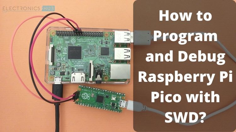
A complete tutorial on programming and debugging Raspberry Pi Pico using SWD Interface. Learn how to Program Raspberry Pi Pico with SWD.
oblique flint
yeah makes no mention of bootsel?
oblique flint
would it still be an issue if I left the pin floating? (not connected to GND)

It's pin 56 right?
distant raven
SWD would be able to directly program the Chip because that’s what SWD is for
oblique flint
that's my schematic
distant raven
Well, I can tell you that you’ll only be able to do XIP programs
RP2040 has no internal flash
distant raven
So XIP instructs it to run on RAM
I’ve designed multiple RP2040 boards, I assure you it needs external flash
oblique flint
ok I'm not familiar with what XIP is. are you saying there's no way to upload a sketch without external flash?
distant raven
So in the Pico SDK you can specify something to do XIP which is execute in place
It loads the program directly into RAM but it isn’t persistent because RAM is volatile memory
I don’t believe Arduino allows this
oblique flint
do you have a flash chip you would recommend in that case?
one that's in stock/reasonably priced right now
distant raven
I found this part with the Digi-Key mobile app. https://www.digikey.com/en/products/detail/W25Q80DVSSIG/4836572
Winbond is the brand they did their design around so it stands to reason this would work just fine
oblique flint
Yeah I was just looking at the schematic and it's the same brand
well.. would be nice to at least test my current board without having to re-order.
Would the fact that I left my BOOTSEL pin floating be bad for SWD @distant raven ?
or is there still a chance I can program this prototype with SWD "xip"
distant raven
It might, mostly because it controls the SPI flash CS pin. It might cause troubles for you. Still worth trying to program at least.
oblique flint
alright thanks for letting me know
 silent plover
Hello ,Can somebody help me with my circuit ?
i try to simplify my circuit but
i don't know if it is correct to do that
 distant raven
I am thinking of making an RP2040 + W5100S-L Ethernet board. Any considerations I should take aside from the obvious impedance/length matching differential pairs, and whatnot
 rancid lagoon
silent plover
i try to simplify my circuit but
rancid lagoon
silent plover
i try to simplify my circuit but
Looking at it the only thing i can see is swapping the ds1302 for a ds1307 or pcf8523 that uses i2c
silent plover
Yes but i only got the ds1302 so i can't do that right now
rancid lagoon
Other than that there is not much you can do
 alpine slate
Hey Guys! I would like to make a custom RP2040 board but i have not yet made a PCB before. I would like a bunch of push buttons, a 240x240 LCD, A USB C Port and 16MB of flash. How hard would this be to design for a beginner? Is there someone experienced with RP2040 boards that takes commissions? Thanks!
supple pollen
alpine slate
Hey Guys! I would like to make a custom RP2040 board but i have not yet made a P...
While it's not a super hard board, it would likely be frustrating for a beginner. Not only do you have to lay out the board, you have to choose the components and assemble it (or have someone else do so). There is an AdaFruit jobs board where you can post requests for designs like this.
alpine slate
Yeah assembly is what im most concerned about because of the smd component
supple pollen
Many board houses also offer assembly. Generally it's easier if you choose parts they have on hand or are available from a particular supplier (such as LCSC). Some will procure parts from vendors such as DigiKey for you, in most cases you can also get the parts yourself and send them to be installed (I've done this with obscure parts). I don't know offhand if any board houses stock RP2040 or if not, what the options are. That said, the tricky parts are likely the USB-C connector wiring (it has to be right or it won't work), the LCD display and attachment, and any firmware issues related to the 16MB flash.
distant raven
Overall though, definitely possible


Lol
Just put 16MB flash and that’s basically it
alpine slate
Well thats pretty much exactly what i need lol
worldly schooner
alpine slate
Hey Guys! I would like to make a custom RP2040 board but i have not yet made a P...
Putting an RP2040-based design together in EDA software like KiCAD or EasyEDA is relatively straightforward, especially when Raspberry Pi foundation provides a hardware design guide (https://datasheets.raspberrypi.com/rp2040/hardware-design-with-rp2040.pdf) for specifically the RP2040. It does take a significant amount of learning to properly use the EDA tools, but the design portion isn't bad if you're comfortable selecting components. The USB-C port is fairly simple to implement too, if all you need is USB 2.0 and none of the extra sideband or USB3 functionality that the RP2040 wouldn't support anyways. Worst case scenario, you could even import an open-source RP2040 design and make your additions to that. Adafruit has all of their original designs available in their github; Eagle files for anyone using that particular CAD software, and schematics/PCB layouts in pdf format for everyone else. Take the Feather RP2040, for instance: https://learn.adafruit.com/adafruit-feather-rp2040-pico/downloads
Getting a PCB made and fabricated is also pretty easy. With more and more online PCB manufacturing quoting services like JLCPCB and PCBWay, you can get reasonably priced custom boards fairly hassle-free. The options can be overwhelming at first, but the default options are typically sufficient in the absence of a particular need. Just make sure that your boards pass the DRC rules your manufacturer sets, not just the default rules set in your EDA.
The hardest part of PCB design isn't getting a board made. It's validating a design and making sure it works, or fixing it and revising it if it doesn't. Usually even veteran PCB makers will let mistakes slip through fabrication, but with some trace cutting and/or bodging, they can establish the fixes needed for the final board version. We might not be able to guarantee we can find everything, but this channel usually has a couple of gurus around to take a first pass at any schematics or PCB layouts if you're not confident. If something does slip through, though, I hope you're handy with a soldering iron, haha.
Though if you're using an existing design like that one, you should pretty much be set...
alpine slate
Thanks for that explanation mate!
worldly schooner
@distant raven is that your original design?
distant raven
worldly schooner
<@728676724522352733> is that your original design?
It’s a board I threw together yesterday in like 3 hours
alpine slate
I want to look the pcb like this. Not all of the buttons but still. And then ill 3D Print the case
 distant raven
👀
worldly schooner
Oh, that's a LOT of buttons.
distant raven
Like like a MacroPad?
alpine slate
No im writing a tinyyy „flight sim“ with airbus systems. Very simplified to run on the RP2040
distant raven
Ohh neat
alpine slate
Yeah!
Say, would incorporating all those buttons even be possible? I assume even a Button matrix would be struggling no?
distant raven
Oh heavens no
alpine slate
Yeah thats what i thought
distant raven
The MacroPad RP2040 is pretty quick 🙂 so yours should be more than capable
knotty tiger
that's not a much larger number of buttons than a full PC keyboard, it looks like, and those are typically wired as a matrix
worldly schooner
With a button matrix this should be just barely manageable. 8x10 buttons would use 18 GPIO, leaving you enough pins for the display. Any more though, and you should consider using a GPIO expander instead.
worldly schooner
knotty tiger
that's not a much larger number of buttons than a full PC keyboard, it looks lik...
There really aren't a lot of 104-key RP2040 designs. Most stop at 87 max.
alpine slate
That was just a thought - I wont nearly need nearly as many. Realistically i will only need 4-5 buttons.
worldly schooner
It's possible with some creative arrangement, but it's really tight.
knotty tiger
you maybe could charlieplex the matrix to halve the needed GPIOs, but that makes the firmware more complicated and error-prone
worldly schooner
Nah, assuming you're using a dumb slide switch for on/off, you have a couple more GPIO to spare. 18 GPIO for up to 80 buttons, 4 GPIO for an SPI display, and a couple for VBUS monitor functions and the like.
Actually, scratch the switch comment. 80 buttons is more than manageable.
alpine slate
Am I mistaken if i think that the pico is really capable? Ive heard people say its underpowered but the fact its running doom and other stuff proves otherwise. Im not nearly as experienced to judge this
worldly schooner
Doom isn't the best bar to use for a performance comparison, but the Pico is pretty good at what it does.
distant raven
RP2040 is very capable for a Cortex M0
What really helps is it’s 125MHz clock and two PIO registers
And it has a bunch of RAM compared to most cortex M0
knotty tiger
people are writing what look like useful logic analyzers based on RP2040 using PIO
alpine slate
Im just hoping the pico will handle my flight sim thing
worldly schooner
Underpowered is relative. It has its weaknesses, for sure, like the lack of floating-point hardware. If your flightsim needs a lot of floating point calculations, you should pick something better suited for that. For a bunch of buttons and a display, its fantastic.
alpine slate
worldly schooner
Underpowered is relative. It has its weaknesses, for sure, like the lack of floa...
Im avoiding floating point where i can already lol
distant raven
Or you can do floating point approximation if you need it. A little resource intensive but doable on the Pico
alpine slate
Yeah
Considering the aircraft will fly itself and the nature of its flybywire systems it’ll be so simple that - if you flew it via hand - it would be like on rails. But Airbus airplanes are basically on rails anyways.
worldly schooner
I know very little about flightsims, so I'll leave those design decisions to you haha
knotty tiger
you're simulating the FMS, not the actual flight controls?
alpine slate
Oh no not the FMS. Im writing a very, very simple flight „sim“ in which the airbus can fly itself. Im writing all of its main system, the FMS not being included. Mostly elec, hyd, flight control systems and other small goodies
alpine slate
worldly schooner
I know very little about flightsims, so I'll leave those design decisions to you...
Im a flight sim addon developer and Ive kinda fallen in love with the A320. Been researching everything about it, got official documentation. Im now making a 3D Model of it and making this tiny simulator
knotty tiger
nice
alpine slate
@knotty tiger Are you into aviation at all?
knotty tiger
alpine slate
<@824013908490059826> Are you into aviation at all?
somewhat. i did an aero/astro major but not much on actual piloting or flight ops. a few hours of private pilot training. i've never worked in the field
alpine slate
knotty tiger
somewhat. i did an aero/astro major but not much on actual piloting or flight op...
Awesome! I would love to do aviation as a living in the future. Though im not sure if I am going the pilot route because of the current state in aviation
alpine slate
distant raven
Overall though, definitely possible
I assume you’ve used one of those 1.3inch displays before. How do you like them? I want to buy one for my project. The 1.54 inch are too expensive in comparison.
distant raven
They’re pretty good
I will say, refresh rates on TFT SPI displays are not amazing
But they’re usually pretty sharp
alpine slate
distant raven
I will say, refresh rates on TFT SPI displays are not amazing
What’s the average?
distant raven

I think 12-15fps is pretty standard
But color wise, they are great
I think you could probably squeeze 20fps
Just depends on you do your mapping
alpine slate
Is it a limitation of the rp2040 or the display?
distant raven
Display itself
alpine slate
I see
distant raven
In that you can only send so much data at a time
alpine slate
Designing the pcb would be very cool. Im just thinking if im up to the task and how i can get it assembled. Ill look into it.
distant raven
A parallel bus display would be a lot faster refresh rate but it takes A LOT of memory to drive those which is where the RP2040 would likely be slow
For the display, definitely get an FPC connector
It’s easier to solder than worrying about burning the ribbon connector of a display
distant raven
You’ll want to use solder paste, a stencil, and a microscope/magnifying glass
I’ve done compact designs with 0603 parts which are small but fairly new assembler friendly
And for pasting, I wouldn’t be worried about wasting paste, I would do a few practice runs working on getting a good technique so you avoid as many problems as possible during reflow
And make sure you have flux on hand too as it will help if you need to rework
Solder paste will require a hot plate at a minimum to cook
So if you’re able to keep your design to one side of your PCB, that’s ideal
inland jungle
what are the good/cheap SPI displays?
unreal flax
inland jungle
what are the good/cheap SPI displays?
You'll probably want to narrow that down a bit to get good suggestions... Are you looking for one-inch monochrome or 24-inch color? 😉
inland jungle
yeah, sorry, directly referring to the above discussion about 1.3" - 1.5"displays
whether there is a specific brand/source that is recommended
worldly schooner
https://www.adafruit.com/product/4520 would probably be the nicest 1.3" I know of, but you can definitely go cheaper via AliExpress/Amazon...
https://www.amazon.com/HiLetgo-Colorful-Display-128X128-Replace/dp/B073R6SQRY/ref=sr_1_19?keywords=spi+display&qid=1656344301&sr=8-19 looks like it would be my go-to for something cheaper AND prototype-ready, but in the context of PCB design there's definitely cheaper.

HiLetgo 1.44" Colorful SPI TFT LCD Display ST7735 128X128 Replace Nokia 5110/3310 LCD
The resolution is lower, but that might not be a bad thing if framerate is a priority.
split obsidian
Anyone know of these LED holders for 3-4 pin LEDs (for Red/Green or RGB LEDs?) I'm looking to make a single LED indicator on a 3d printing project and idk where to get these nice nice holders for more than two pin LEDs.

 tranquil stirrup
split obsidian
Anyone know of these LED holders for 3-4 pin LEDs (for Red/Green or RGB LEDs?) I...
tranquil stirrup
split obsidian
Anyone know of these LED holders for 3-4 pin LEDs (for Red/Green or RGB LEDs?) I...
it looks like the plastic insert is the only thing making them 2 pin? maybe 3d print a replacement?
split obsidian
If it wasn't so small I would. This is a perfect use case for a resin printer I don't have lol
tranquil stirrup
i think you could redesign it to work. a hollow tube with a cross at the top
or even no cross at all, just a tube would probably be fine
1 sec, let me mock this up using an rgb 5mm as reference
worldly schooner
As long as you insulate the pins inside the tube, a hollow tube should suffice? An FDM printer with 0.4mm nozzle could probably do it with a single wall.
inland jungle
looks like ~0.5mm spacing between the leads on a 5mm 4 wire LED
tranquil stirrup
looks like theres enough clearance for 2 walls
worldly schooner
You probably don't need any inner support, just wrap the two inner pins with heatshrink or electrical tape.
inland jungle
that's additional work/steps, would be nice to just be able to print drop-in replacements
wheat moon
Afternoon everyone 🙂
Question about using the nrf52840 bootloaders for a custom board
tranquil stirrup
 wheat moon
I'm able to load one of the bootloaders, and can see a lot of functionality working: The LED is flashing and I can reset the board.
silent plover
distant raven
awsome
wheat moon
But I'm not seeing the device appear as a USB MSD when plugged in.
I'm curious if I need to adjust the USB_DESC fields in board.h
Specifically these:
(Dyno bot is going a bit ape)
ugh
#define USB_DESC_VID 0x239A
#define USB_DESC_UF2_PID 0x0087
#define USB_DESC_CDC_ONLY_PID 0x0088
Not sure if those are correct, or if they're even relevant.
(PS, sorry to just barge in, didn't mean to disturb the previous conversation)
tranquil stirrup
inland jungle
that's additional work/steps, would be nice to just be able to print drop-in rep...
my printer could print this but you might need to play with slicer settings. thin walls, tolerance settings, etc

Let me know if you want to try it and i can send the 3mf
inland jungle
where did you get the initial model cone?
tranquil stirrup
I measured the bottom of a 5mm rgb led
this probably isnt correct lengthwise and might need tolerances adjusted for the real thing
inland jungle
yeah, the real spacer has a taper on it, one sec I'll measure
10mm tall, 6mm dia. base tapering to 5.5mm dia
tranquil stirrup
I ressessed the insulators a bit to give a little wiggle room at the top. also the diameters are exact so tolerances may be too tight
 inland jungle
I don't have any 4 pin LEDs to test, but it looks nice. According to Amazon, the Edgeelec and Chanzon LEDs have slightly different spacing (1.3mm centers vs 1.0mm) as far as I can tell from their drawings
tranquil stirrup
i have no idea what mine are. i just have a drawer full of them from kits that ill probably never use up
@split obsidian If you want to try printing the part and testing it with an led you have let me know. this should print on an fdm printer with .4mm nozzle if you select the "thin walls" option in your slicer
split obsidian
tranquil stirrup
Let me know if you want to try it and i can send the 3mf
That sounds interesting. I would take the 3mf or pref the f3z (or just a screenshot of the sketch/dimensions would actually be most ideal)
tranquil stirrup
split obsidian
That sounds interesting. I would take the 3mf or pref the f3z (or just a screens...
sent you a request so i can send the link
alpine slate
looking at the rp2040 pcb design guide - its already less of a headache than i thought it would be. So once i have my base pico schematic i "only" need to do the display controller and push buttons.
worldly schooner
alpine slate
looking at the rp2040 pcb design guide - its already less of a headache than i t...
The schematic is basically copy and paste, haha. It gets a bit trickier when you get to layout, but overall should be fairly manageable, even for a beginner.
distant raven
worldly schooner
The schematic is basically copy and paste, haha. It gets a bit trickier when you...
I think the easiest cortex m0 to layout is the samd2x chips
3 caps and 1 resistor
worldly schooner
If only they were available still.
distant raven
Yeah
For shame..
I have 5 left
I have some ideas for what I’m doing with them 🙂
Like interchangeable Neopixel light controller base
supple pollen
distant raven
I think the easiest cortex m0 to layout is the samd2x chips
Not the LPC800? 🙂
distant raven
What the external part count?
supple pollen
I don't remember, but it's pretty low (since that CPU iswas available in a DIP-8 package)
distant raven
Interesting I did see that in the Google results but I guess they obsoleted the dip
supple pollen
Alas, yes.
alpine slate
worldly schooner
The schematic is basically copy and paste, haha. It gets a bit trickier when you...
Yeah and adafruit has schematics for the display driver aswell. Super!
supple pollen

If you like the speed and simplicity of ARM Cortex M0+ chips, but want to just dip a toe in, you'll fall in love with the adorable little LPC810. This particular chip in DIP8 really ...
distant raven
You can put an NFC antenna on this one: https://www.mouser.com/ProductDetail/NXP-Semiconductors/LPC8N04FHI24Z?qs=wd5RIQLrsJjQIhbI9wmb1A%3D%3D
Not terrible for a $4 single
supple pollen
Kewl. TI makes an NFC version of their MSP430 line that can be powered by NFC.
distant raven
Yeah I did see that, pretty cool
wheat moon
Afternoon all,
Still trying to build and flash the bootloader onto my custom PCB. Have made some forward progress, but still running into this error:
Create feather_nrf52840_sense_bootloader-0.6.4-dirty.hex
Create feather_nrf52840_sense_bootloader-0.6.4-dirty_nosd.hex
 - Cannot openmake: *** [_build/build-feather_nrf52840_sense/feather_nrf52840_sense_bootloader-0.6.4-dirty_nosd.hex] Error 1
make: *** wait: No children.  Stop.
make: *** Waiting for unfinished jobs....
make: *** wait: No children.  Stop.
Any guidance on what's happening and how to proceed would be helpful.
distant raven
wheat moon
Afternoon all,
Still trying to build and flash the bootloader onto my custom PC...
Have you tried using the Adafruit DAP library?
wheat moon
I'm not sure what that's for, tbh
distant raven
so DAP is roughly Direct Access Programming
it uses an arduino capable board like a feather M4 as a CMSIS programmer over SWD

GitHub
port of free-DAP to standalone arduino. Contribute to adafruit/Adafruit_DAP development by creating an account on GitHub.
there's this example here that you would just replace the 40_BOOT.bin file with your BIN that you create
have you been able to create a binary for your nRF52840 board?
wheat moon
I haven't tried. I've been attempting to follow the information on the bootloader github page

GitHub
USB-enabled bootloaders for the nRF52 BLE SoC chips - GitHub - adafruit/Adafruit_nRF52_Bootloader: USB-enabled bootloaders for the nRF52 BLE SoC chips
distant raven
gotcha
distant raven
I’ve not built that yet but I’ll probably fork it because I am going to try and use something similar for my smart watch that has an nRF52811
wheat moon
Very cool!
Honestly, this seems like a tiny hiccup
hmmm.. I may have found a solution lol
distant raven
Oh good!
distant raven
Oh dang
wheat moon
Ok. I can build it using WSL, then flash it by exiting back out to windows
That's fine
Sadly, the device's MSD still doesn't appear over USB
distant raven
Dang, that’s no bueno
 twilit mango
That's what happens if you're working with altered files that haven't been merged into anything, iirc.
It's a Git term.
wheat moon
I see - so it's because I've redefined some button designations?
twilit mango
wheat moon
I see - so it's because I've redefined some button designations?
That would do it.
wheat moon
Thanks Kattni 🙂
twilit mango
You're welcome!
wheat moon
hmmm... interesting
it seems I can now see my board using NRFConnect
That's new!
Weird.
wheat moon
Pre-certified module?
This is strange: I'm trying to push the bootloader for the Feather Sense to my PCB. I use the exact same SOC as the Feather Sense, but the NRF Programming module is telling me part of the hex regions are out of the device's memory size.
distant raven
Strange
Pre-certified module is like a module that has the chip and required components, usually an antenna or u.fl connector for an external antenna
wheat moon
Nope, this is all custom built.
distant raven
So you bought the raw chip, picked your antenna matching network and whatnot?
wheat moon
The hardware team did
wheat moon
I sat those meetings and advised them on which SOC to use so we could proceed with CPy
wheat moon
distant raven
So you’re just doing firmware then?
Yes
distant raven
Well, either way; pretty cool stuff
wheat moon
Interesting: I can make and push CPy for the nrf52840 DK
Doesn't work right (doesn't show as a device via USB)
distant raven
I designed this RP2040+nRF board
 wheat moon
Our design is much closer to the feather
distant raven
Makes sense
wheat moon
distant raven
I designed this RP2040+nRF board
Nice! Congratz 🙂
distant raven
Feather is a great format
wheat moon
Wondering which board definition is closest to the feather
I don't see one explicitly made for the feather sense in the ports
distant raven
Try loading that 40_BOOT.bin that’s in the Adafruit DAP library I shared
From what I understand it’s a prebuilt binary that is verified to work
Also look at the readme in the example
wheat moon
That's problematic - I need to change some of the GPIO definitions
distant raven
There are two sets of data that need to be written to the nRF when programming that are likely not in the binary itself
GitHub
port of free-DAP to standalone arduino. Contribute to adafruit/Adafruit_DAP development by creating an account on GitHub.
Not sure if that would be helpful or not
wheat moon
Might be
1 sec, reading ;l)
😉
ok
when I run that I get make: *** No rule to make target 'combinehex'. Stop.
distant raven
Inside the nRF52 bootloader library?
distant raven
Lol
distant raven
Yeah
distant raven
Strange
wheat moon
Do you happen to know which board definition I would use to build CPy for the feather sense using the general repo?

GitHub
CircuitPython - a Python implementation for teaching coding with microcontrollers - GitHub - adafruit/circuitpython: CircuitPython - a Python implementation for teaching coding with microcontrollers
distant raven
GitHub
CircuitPython - a Python implementation for teaching coding with microcontrollers - circuitpython/ports/nrf/boards/feather_bluefruit_sense at main · adafruit/circuitpython
Probably bluefruit sense
wheat moon
ok, trying that 🙂
I'm assuming it includes the bootloader - perhaps that's a wrong assumption.
distant raven
UF2 should just have the circuitpython program. I’d you got the bootloader on and usb msc then it might work
wheat moon
ok, so it doesn't make sense to build this and push
Ok. The main issue appears to be that the bootloader is being pushed to an area outside my SOC's memory. That's strange to me given that we're using the same SOC as the feather sense.
distant raven
yeah, it is strange
 signal topaz
Can anyone suggest some inverting converter or other power solution for negative voltage of around -7.5V and min. 1A output current? I like TPS63710 but it's limit is -6V.
alpine slate
KiCad is so complex 💀 its gonna take some time for me to understand any of that before i even try to make my design
limpid nest
I'm looking at guides/info about gate resistors for mosfets. This one guide calls for 1k Ohm, does that seem high? Their logic makes sense but a long time ago I spec'd 100 ohm (I don't recall why). Thoughts?
On the same subject, it seems truly calculating a pull down resistor for a mosfet is an in depth procedure, does anyone have any tips/rules of thumb?
oblique flint
Anyone here have experience designing PCB test fixtures with button actuators? Meaning, making physical actuators that test the buttons of a PCB. Or know any guides relating to this?
 hushed smelt
saw the teensy 4.1 has a place to add more ram and flash. wondering can i take my existing feather for example and drop a larger flash or ram chip on it if it's the same pad type or does the mcu only recognize a certain amount? i'm continually running out of memory on my bluefruit sense with a graphically heavy project. how much is too much? never, enough. i have a 250gb sd card on a featherwing i'd rather have too much than not enough.
 teal storm
why is EAGLE annoying
i want to work on the schematic for my pcb but it says its not linked
i did all the work i can on the board but when i generate the schematic it says it wont backannotate
supple pollen
oblique flint
Anyone here have experience designing PCB test fixtures with button actuators? M...
While I haven't done so, I'm thinking servos or solenoids might do the job.
teal storm
if i dismiss it then my schematic is empty but my board has stuff on it
oblique flint
supple pollen
While I haven't done so, I'm thinking servos or solenoids might do the job.
The problem with servos and especially solenoids, is they don't have enough torque to press a mechanical button
teal storm
oh
oblique flint
I looked up the switch and it requires 160gf ±50gf to press it
supple pollen
oblique flint
The problem with servos and especially solenoids, is they don't have enough torq...
Depends on the button, the servo, and the leverage. In general, this is a solvable problem.
oblique flint
the other thing I have to take into account is to ensure the button doesn't get over-pressed and damaged as a result
or under-pressed and not actuated as a result
since SMT components can shift slightly, although this button does have alignment pins
supple pollen
That's one reason I mentioned solenoids, which can provide a known amount of force. With a servo, you'd need more of a feedback mechanism to measure force and determine when to stop pushing.
 teal storm
solenoid with a lever so you get the force and a stop so you dont over press
supple pollen
When you said "not enough force", I'll admit I was thinking of a much bigger switch. Even a micro servo can operate that handily.
oblique flint
@supple pollen are you thinking of a 1:1 servo-to-button actuation or some sort of mechanism in between?
supple pollen
I was thinking of pressing the button with a servo horn, but all sorts of mechanisms are possible. You could use a compliant/springy mechanism to control the amount of force delivered.
oblique flint
yeah I was thinking a spring might have to go in between. This is definitely a tricky problem to solve 🙂
it's easy in theory, but meechanically speaking for such a tiny button, requires some precise assembly
supple pollen
You are correct. You have to deal with alignment, slippage, switch positioning, board flexing, software bugs, and a whole host of other ways things could go awry.
oblique flint
the simplest solution is to have the button be pressed by a person and turn on an LED to tell the person that it's closed circuit and working
but relying on humans isn't advisable 🙂
supple pollen
It is often done, as humans are somewhat self-calibrating. https://www.sparkfun.com/tutorials/138
oblique flint
Intersting guide, thanks for the link.
My other concern with a human pressing the buttons manually is they may shift the board while it's inside the jig. But I have yet to test this theory. It of course depends on the pressure the board is held under
inland jungle
Mini solenoid plus a spring is a pretty easy solution
knotty tiger
supple pollen
It is often done, as humans are somewhat self-calibrating. https://www.sparkfun...
accessing that calibration data in a useful way can be challenging, though 😂
limpid nest
limpid nest
I'm looking at guides/info about gate resistors for mosfets. This one guide call...
Asked this yesterday, anyone got an idea?
supple pollen
Do you mean a series gate resistor (limits current in/out of gate, slew rate, and increases turn-on/turn-off time), or a parallel (pull) resistor (determines the gate voltage when it isn't otherwise being actively driven)?
supple pollen
Normally gate charge and gate voltage are fairly small, so it doesn't take a lot of energy to charge/discharge the gate (in DC conditions, the gate draws essentially zero current, so the resistor has no effect: it only does anything while the gate is being charged/discharged). If you're driving the gate with a fairly beefy driver, it's not a big deal. But if you're driving it with a microcontroller pin, you might want to limit the current. If you have (say) a 5V microcontroller and you want to limit the current to 5mA, you simply divide 5V by 5mA and arrive at 1000Ω. However, that current doesn't flow for long (just long enough to charge the gate), so normally you can get away with higher brief peak currents. If you're switching the MOSFET at a high frequency, those pulses are more frequent, but that resistor is also slowing down the charge/discharge: in that circumstance, a gate driver might make sense.
knotty tiger
what kind of MOSFET? and what application?
limpid nest
I'm very periodically charging the gate to turn an LED on. 3.3V micro
speed isn't important
supple pollen
There are other, more subtle reasons for a gate resistor, like damping ringing, but those would normally be addressed by a lower resistor value.
limpid nest
N channel FET
knotty tiger
power or small signal?
limpid nest
let me check
supple pollen
In that case, speed is not of the essence and 1k is probably totally fine (and would limit the current to 3.3mA, which is safe for most microcontrollers).
Having the MOSFET switch slowly is not an issue either, with a 20mA LED, it's not going to overheat by remaining in its linear region longer: that becomes a problem at higher currents and frequencies.
limpid nest
I think it's small signal, it's a 150mW piece
limpid nest
supple pollen
Having the MOSFET switch slowly is not an issue either, with a 20mA LED, it's no...
This is all along the lines I was thinking, thank you. I just don't want to make a mistake
supple pollen
Yeah, I'm guessing a common small MOSFET like a 2N7000, BSS138, or A2SHB
limpid nest
Yeah I went with one with a switching voltage below 3.3V
supple pollen
It's good to understand the "why" of things, so you can know when various things are actually required, and how to calculate them.
limpid nest
Yeah I don't love just throwing stuff in
Like I can do that to get a build finished but then I like to know things
supple pollen
Note: threshold voltage isn't the same as switching voltage: I've seen people have problems switching MOSFETs with 3.3V when the threshold voltage is listed as 2V max and the MOSFETs weren't conducting well.
limpid nest
yeah it's 1.25/2.5 or something like that
I'm aware of that trap thankfully
min RDSON is 2.5V
knotty tiger
the datasheet should tell you things like gate capacitance, in case you want to do calculations about switching transients, etc.
supple pollen
limpid nest
min RDSON is 2.5V
That's a good spec. I'm curious which one that is.
supple pollen
Nice find, thanks!
limpid nest
np!
limpid nest
How do you do a multi color silkscreen like this? https://www.adafruit.com/product/5495
teal storm
im using EAGLE and my board wont do the back-annotation thing that the others do. i cant get it to generate a schematic from the board and i dont know how to fix it. please help.
ping me if you can help i probably wont see it if you dont
limpid nest
Do resettable fuses come in standard packages?
worldly schooner
limpid nest
Do resettable fuses come in standard packages?
Much like other SMD passives, SMD fuses come in many different sizes, from 0402 up to maybe 2920? You should check your current requirements, though, as higher currents typically need larger packages.
limpid nest
worldly schooner
Much like other SMD passives, SMD fuses come in many different sizes, from 0402 ...
Sorry I didn't say my full thoughts, I'm looking for a 3d package/step. I've already sized it.
worldly schooner
limpid nest
Sorry I didn't say my full thoughts, I'm looking for a 3d package/step. I've al...
What size?
limpid nest
worldly schooner
What size?
I found one, sorry, forgot to respond! 1812
teal storm
teal storm
im using EAGLE and my board wont do the back-annotation thing that the others do...
Am I invisible
inland jungle
if people don't know how to help you with you're problem, they generally won't respond. so try to be patient. When using Eagle, I've never tried to go from board to schematic. I don't think it's even possible in Eagle
limpid nest
I'm doing a power input ->diode to drop a voltage a bit. Is it worth it to try to make a custom power symbol? I've never gotten it to work in the past
glacial gale
so hardware caches take like 80% of the transistors on a chip
does it make sense to fabricate a prototype cpu without the cache
for testing
distant raven
glacial gale
does it make sense to fabricate a prototype cpu without the cache
Not really, the goal of cache is speed due to proximity
Take it away, and you’re limiting how well your CPU performs
glacial gale
thats true, but maybe you could just scale the cache back by 90% to see how the cpu works in general. Idk if amd/intel does that but I think its quite problematic to have such huge dies
distant raven
glacial gale
thats true, but maybe you could just scale the cache back by 90% to see how the ...
It’s not necessarily avoidable. Speed comes from proximity and size of cache and how many instructions are needed to fetch data into cache. Smaller cache severely limits speed and will bottleneck your performance greatly
inland jungle
what do you mean by problematic? it's one of the most straightforward ways to boost performance
 heavy jasper
These days for the big players I suspect the chip may not work nearly as expected without the local caches available - but they also build in a million ways to tweak things on the fly if needed. Even on MCUs I have seen bad cache implementations cause problems (especially when there are hardware peripheral addresses that specifically must not be cached also around). For the big players, I suspect there’s not a reason to build a full CPU chip any way other than the full “we expect this to work” variant - die runs are horrifically expensive, and they just do enough design validation to have confidence that it will either work, or have failures that can be contained well within their various on-the-fly tweaking tooling.
Like - even physical placement of the circuits on the silicon is quite important, so building up a whole solution without a huge chunk of your area (and all of its interconnects) accounted for is a recipe for some pain later.
distant raven
inland jungle
what do you mean by problematic? it's one of the most straightforward ways to bo...
For a moment I thought you were asking me 😂
distant raven
heavy jasper
These days for the big players I suspect the chip may not work nearly as expecte...
This is probably also why FPGAs are so critical to validating architectural modifications and enhancements. While not perfect, allows for cheaper proof of concept testing.
I took some graduate level course work on VLSI and Verification so my knowledge is somewhat there.. hehe.. I need to do more though because I do love computing architecture
inland jungle
I did an undergraduate course probably about 25 years ago, so my knowledge is definitely not there 🙂
teal storm
limpid nest
I'm doing a power input ->diode to drop a voltage a bit. Is it worth it to try t...
Just go to the supply1 and supply2 lib if ur using EAGLE. Pick out the one with the correct voltage and use that. It automatically links stuff which you probably already knew
limpid nest
when looking at an open collector output, how does one pick a pullup resistor? I found this source https://www.ti.com/lit/an/slva485/slva485.pdf?ts=1656689465579&ref_url=https%253A%252F%252Fwww.google.com%252F but the datasheet for my part doesn't specify a leakage current. Can I just use 10k and call it good?
supple pollen
It normally depends on the voltage you're pulling up to, and the impedance of whatever you're driving, more than the leakage in the open-collector output.
limpid nest
Hmm
supple pollen
Slew rate and distributed capacitance can also be a factor, depending on waveshape and frequency.
limpid nest
I'm pulling to 3.3 and driving a high impedance input of an mcu
Frequency is low, should be "square"
So how can I figure out the I into the MCU pin?
this app note says it's just in the datasheet, but doesn't it depend on the voltage seen by the pin?
knotty tiger
sometimes the datasheet will have a pin input capacitance, but also, wiring or PCB distributed capacitance can be larger
supple pollen
Yeah, 10k is fine.
Most modern MCUs are CMOS and have high impedance inputs (although some have built-in pull-up resistors you can turn on)
limpid nest
thanks folks
 vapid cradle
i'm looking to build a solar powered rover for my nature cameras. i already have 2x 100w panels, 2x 100Ah SLA batteries in 24volt, a solar charge controller, wifi, cameras, sitting out in my field and it all works fine. i'd like to put this existing setup on a mobile platform so that i can drive it around and look at different things 🙂 currently, the gear is around 50kg (mostly the 2 SLA batteries). i'm looking for some motors + motor controller that can move that much mass. it doesn't need to move fast. i'd like to power it via the 24 volt batteries, and if possible, i have an extra raspberry pi that i'd like to use to drive it - i'd like to code up a small website where i (or others) can send the commands, move the cameras, etc.
teal storm
i would go with a tracked vehicle because they are easily driven with only 2 sets of motors and are mechanically simple
and good at medium terrain maneuverability
vapid cradle
what kind of motors should i look for that can move 50+ kg?
teal storm
big
a set of mekanum would maybe be better because you can move linearly on all axes except upwards
forward back, left right, and all the diagonals as well as on the spot rotation and 2 and 3 point turns
vapid cradle
this will be outdoors, i'm pretty sure mecanum will get stuck?
teal storm
fair point
vapid cradle
i was looking at 4 or 6 big wheels, around 8" diameter since that's what i can 3d print. i'm also thinking about tracks as you mentioned, but for a v1 i think wheels might be easier?
teal storm
I dont think they would be because you just make 2 holes on either side and put bearings in them, stick an axle in and put some sprockets then power some of the axles
vapid cradle
pardon my ignorance, but with either wheels or tracks, would the motor be the same?
or motors, rather, as i'm imagining i
i'll need a few*
teal storm
Would you do tank steering with the wheels or awd and front wheel steering or some other combo
Like awd and rear wheel steering
vapid cradle
skid steer yeah, with wheels or tracks
or rather, i was going to use 1 motor per wheel. but with tracks, if i only need like 2 motors...
teal storm
It would be the same which means you could make both and test them and use the letter one
I meant better
Also a motor on each wheel or a motor on each side would work for both
So 2 or 4 or 6 even it doesn’t matter as long as the sides are even
But I gotta watch a movie rn so I gtg
vapid cradle
i really want 4 motors i think - 2 on each side. for more power and a little redundancy
teal storm
Yea
vapid cradle
no worries, appreciate it 🙂
limpid nest
vapid cradle
i was looking at 4 or 6 big wheels, around 8" diameter since that's what i can 3...
I wouldn't do printed wheels for this
rancid lagoon
if you are going to print them use 100% infill
teal storm
https://www.adafruit.com/product/2719 yo is there a download for this for EAGLE
If you've been diggin' our monochrome OLEDs but need something bigger, this display will delight you! These displays are 2.42" diagonal, and very readable due to the high ...
distant raven
teal storm
https://www.adafruit.com/product/2719 yo is there a download for this for EAGLE

Adafruit Learning System
Ready-to-go monochrome OLED modules with 128x64 white pixels
teal storm
Nothing here says EAGLE files or anything. It’s just the diagrams and data sheets

I’ve gone through that pages contents like 5 times now and I don’t see it
But also it’s almost midnight here so I need to not be on discord rn
distant raven
Looks like these are from before they put the schematics and eagle files on GitHub
I’m also not 100% convinced Adafruit manufactured that board
I think it’s just one they sold
Other 128x64 OLED (like the 0.96” version) has its files on GitHub
supple pollen
Do you need the Eagle files to connect to it, or for the board itself?
teal storm
To connect to it and see if the board fits on my existing board
supple pollen
It looks like it's just a row of 20 connections on 0.1" centers.
teal storm
is there a logic gate that just outputs whatever is inputted but only if it has power from a second input
like a passthrough
it sends through the input if it has power on a certain pin
distant raven
teal storm
it sends through the input if it has power on a certain pin
And AND gate?
Put a voltage level comparator on one gate and your signal on the other
Use the comparator to see if the voltage meets the threshold to pass a logic 1 to the AND gate
teal storm
no but an and gate outputs HIGH if it gets two HIGH inputs but this passthrough would output 1.765 volts if that was the input and it had 5v on the allow passage pin
like an actual gate
IN is equal to OUT as long as EN is 5V
if EN is not 5V then OUT is ground no matter what IN is
IN = 3.882742V, EN = 5V, OUT = 3.882742V
IN = 3.882742V, EN = 0V, OUT = 0V
its a transistor
nvm
NPN or PNP though
knotty tiger
turned-on MOSFETs act more like resistors than bipolar transistors (NPN/PNP) do. there are also specialized analog switch devices
inland jungle
opamp buffer with an enable
alpine slate
Guys Im still going back and forth with my PCB Idea. Since im a beginner, what would be easier and cheaper? Making a full custom RP2040 board or just making a board that i solder a pico to.
supple pollen
alpine slate
Guys Im still going back and forth with my PCB Idea. Since im a beginner, what w...
Probably easier to solder a pico to a board. I do that too sometimes (like this Teensy I used as a socketed daughterboard). Dunno which is cheaper.

One advantage to that approach is you can sometimes go for cheaper boards (particularly fine pitch boards cost more to make, and generally the boards I make can go for cheaper 6/6 or even 10/10 spacing).
distant raven
this is more of a sanity check. I've got some 12MHz crystals and 27pF load capacitors that go with the 12MHz crystals, should that been good enough for this SAMD51? seems to fall pretty close to what they say you can use.

12MHz falls in the 8-48MHz range they want and load capacitance is pretty close to 26pF
supple pollen
The correct load capacitance depends on the load the crystal is designed for. This blog post offers a good explanation: https://blog.adafruit.com/2012/01/24/choosing-the-right-crystal-and-caps-for-your-design/
distant raven
supple pollen
The correct load capacitance depends on the load the crystal is designed for. T...
I know that bit as I reference that article a lot when picking load capacitors for my crystals. I’m just making sure I’m not overthinking. The 12MHz crystal I have needs ~27pF load capacitors which is why I’m thinking about using it because microchip seems to want crystals that need 26pF load capacitors.
I’m sure any appropriately picked crystal/load capacitor combo would function fine. I guess I’m just curious why they might specify that you should pick a crystal in that range with the specific load capacitors
Perhaps the performance is better with crystals that use 26pF capacitors. I’m probably just wanting more details than the data sheet really has to offer
Or than is really necessary to think about
supple pollen
The main issues are startup time and frequency accuracy. For this use case, I don't think either is critical.
distant raven
supple pollen
The main issues are startup time and frequency accuracy. For this use case, I d...
Fair, figured it was worth an ask. This design attempt will be fun because it’s the TFBGA package samd51p19a
It’s the only samd51 in stock so I figured, might as well try
It’s a pretty nice footprint for a BGA
This is the ball pattern

0.5mm pitch, 0.25mm pad
Possibly making a feather out of it
Probably need to add support to the uf2-samdx1 repo to make a usb msc bootrom for it
Though I think what they have might actually work fine
Yup, look at that! Already support 🙂 https://github.com/adafruit/uf2-samdx1/blob/master/lib/samd51/include/samd51p19a.h

GitHub
MSC bootloader (based on UF2) for SAMD21. Contribute to adafruit/uf2-samdx1 development by creating an account on GitHub.
glacial gale
how feasible would it to make something like https://github.com/furrtek/DMG-CPU-Inside/blob/master/Schematics/dmg-cpu-b_schematics.PDF from scratch?

GitHub
Reverse-engineered schematics for DMG-CPU-B. Contribute to furrtek/DMG-CPU-Inside development by creating an account on GitHub.
distant raven
glacial gale
how feasible would it to make something like https://github.com/furrtek/DMG-CPU-...
Using transistors or an FPGA?
And by transistors I mean using cmos 74xx chips for handling gate logic
You could probably design a lot of PCBs together to make this with cmos logic
Probably be easier on an FPGA
glacial gale
yea on an fpga. Then I guess one could convert that into a simplified design for lithography
 warped stratus
So I've been feeling nostalgic getting into very retro computing and have been learning about the very first microcomputers, for example the IMSAI 8080 and the S100 bus. It's interesting to see how backplanes became the expansion card systems we use nowadays. So I had this thought. Wouldn't it be interesting to merge old and new technologies, make an old-school card for a newer computer. Make something silly like a TMS9918 graphics card for the PC.
So I started with the idea of making a PCI-E break-out card to learn how to make PCBs, but when I looked at the pin out, it's not obvious how you break out the address and data lines from the CPU. I was thinking of doing it old-school where I would write data to addresses, but with the convenience of having newer tools to use in Windows.
How do you get into making PCI-E cards?
supple pollen
warped stratus
So I've been feeling nostalgic getting into very retro computing and have been l...
Amusingly, my first computer (which I still have) is a 6800 board with a converter to support S100 peripherals. Making PCI-E boards isn't particularly tough, just you'd have to specify a "hard gold" process for the contact fingers, which would increase the price somewhat.
alpine slate
Does anyone know if this board would fit on a pcb for a pico?

 steep timber
Hi - just wondering - how would you connect e led strip of 10 ws2812b to KB2040? will 3v3 be enought o power it?
worldly schooner
alpine slate
Does anyone know if this board would fit on a pcb for a pico?
It looks like it would. Pinouts mostly match as far as I can tell, so as long as the back is flat, it should work?
knotty tiger
steep timber
Hi - just wondering - how would you connect e led strip of 10 ws2812b to KB2040?...
voltage-wise it seems likely to work. you might need to be careful about exceeding the max current from the 3.3V regulator? don't light them all up at full brightness at once
steep timber
knotty tiger
voltage-wise it seems likely to work. you might need to be careful about exceedi...
hm... gotcha. Thanks ;]
worldly schooner
steep timber
Hi - just wondering - how would you connect e led strip of 10 ws2812b to KB2040?...
You could try it, but WS2812B is not guaranteed to work well at 3.3V. The chip calls for minimum 3.5V, anything lower and you might not get all of your colors.
An SK6812 strip would work much better, if you can find one?
steep timber
I'm considering ws2812b or SK6812 mini-e for keyboard backlight - and was wondering if 3v3 will power it - I can go with SK6812 - that's not a problem. ;]
knotty tiger
try it and see? i think you might lose some color depth on the blues, because those LEDs need the most voltage
steep timber
also considering either KB2040 or proMicro for mcu - and KB2040 is mucho bettah then proMicro - except that power issue.
well - as soon as I will get my batch of sk6812's will try then ;]
knotty tiger
you could also run the NeoPixels off 5V if you level shift the data line
steep timber
basic keyboard, so don't want to add any additional hw there ;]
but yeah - that would be an option...
knotty tiger
apparently the KB2040 has a RAW pin that seems intended for high current NeoPixel power (if you bypass the 500mA fuse)
steep timber
hm.... how can I bypass it?
knotty tiger
the learning guide says there's a solder jumper
knotty tiger
i've found NeoPixels to be painfully bright at even 3.3V, so if you're trying to minimize parts count, maybe try it out at 3.3V and see if it's good enough for your purposes
alpine slate
worldly schooner
It looks like it would. Pinouts mostly match as far as I can tell, so as long as...
Thats what i was thinking. Thanks!
knotty tiger
@steep timber there's a low-parts hack for driving NeoPixels off of 5V power with a 3.3V controller: series rectifier diode between 5V and the NeoPixel VDD. it drops the voltage just enough so that a CMOS 3.3V logic high will reach the 0.7 * VDD threshold. i haven't personally tried it yet though. example at https://learn.adafruit.com/neopixels-on-raspberry-pi/raspberry-pi-wiring

Adafruit Learning System
How to control NeoPixel LEDs with Python on a Raspberry Pi!
steep timber
hm.... will that also apply to rp pi pico?
knotty tiger
it seems generally applicable to 3.3V CMOS microcontrollers
 fallow ledge
Not sure if this is the right channel... I'm looking for a chip (preferably on some sort of breakout board) to charge/discharge a 3S Lipo battery for a robot. So it should be able to safely charge the Lipo through USB or similar, and then provide at least 5A output from the battery as well. I tried searching "3S lipo charging discharging circuit" but I've only found "fuel gauge meters" for single-cell Lipos.
rancid lagoon
fallow ledge
Not sure if this is the right channel... I'm looking for a chip (preferably on s...
I don’t know of any boards but searching for something closer to “3S lipo usb charger board” might help
distant raven
I’m not sure there are many cheap options for 3S chargers, my guess is you’ll pay over $50 for one assembled
I’d look for something built around a chip like this one: https://www.digikey.com/en/products/detail/MP26123DR-LF-P/5298224
Order today, ships today. MP26123DR-LF-P – Charger IC Lithium Ion 16-QFN (4x4) from Monolithic Power Systems Inc.. Pricing and Availability on millions of electronic components from Digi-Key Electronics.
This chip do so 2S and 3S Lithium Ion
But the eval boards for these are pretty pricy
worldly schooner
distant raven
I’d look for something built around a chip like this one: https://www.digikey.co...
Step down means you'll need a 13V+ supply, though, so it'll probably need a step-up in conjunction?
Or a USB PD negotiator
distant raven
Yeah, it would need to boost battery supply to 5A
But you can only charge so fast with Lithium Ion without overcharging/overheating
That charger IC takes up to 24V
So realistically you could charge a 25W 3S battery in an hour
I’d go from a 15V USB-C WART to the charger IC
distant raven
worldly schooner
Or a USB PD negotiator
Probably necessary in this case
So just parts and PCB alone probably make this a $15-18 board if made by yourself
So I’d expect to pay probably $50+
I see Amazon has some multi-chemistry chargers for 3S for $40

Lipo RC Battery Balance Charger For 1S-6S Li-ion NiMH NiCD Li-Fe Lipo Battery
How good is it? Uncertain but I would imagine it works decent enough
worldly schooner
distant raven
https://a.co/d/3BtxzdX
Discharge rate max is 2A for this one. 5A is a lot...
distant raven
Yeah, 5A probably isn’t doable. I don’t know that I’ve seen 5A LiPo discharge rates
I’ve not looked deep
But that’s a lot to discharge
Lots of heat
teal storm
is there a component that has 2 inputs (excluding VCC and GND) and one output. if input 1 is high, the resistance between VCC and output 1 goes up. if input 2 is high, the resistance between VCC and output 1 goes down
like an analog counter that can count up and count down
distant raven
I’m not aware of something that acts specifically that way other than maybe an ideal op amp
knotty tiger
generally, analog outputs are designed to act like voltage sources or current sources. acting like a resistor is kind of weird and is subject to various limitations (though there are digital potentiometers that kind of do that, again, they have limitations)
worldly schooner
teal storm
is there a component that has 2 inputs (excluding VCC and GND) and one output. i...
A single component, no, but it might be possible to create a circuit to accomplish this with a resistor ladder and multiplexers?
fallow ledge
distant raven
I’m not sure there are many cheap options for 3S chargers, my guess is you’ll pa...
I'm looking for something more like this [https://www.robotshop.com/en/lipo-rider-plus-charger-booster-5v24a-usb-type-c.html?gclid=EAIaIQobChMI2-S4m_7h-AIVSs-GCh1gHQj3EAQYCyABEgJs2PD_BwE] but it works with 3s lipos. So charging and discharging
worldly schooner
USB is a pretty common source for 1S, as the 5V is perfect for easy charging of a 3.2-4.2V battery. Charging an 10.8-12.6V battery is significantly more complex, requiring higher voltages and more protective circuitry.
Also, even this isn't rated for discharge of more than 3A at a time. 5A discharge is a lot of current for an integrated system.
distant raven
You need highly specialized chargers to discharge more than 2-3A
And it’ll cost you a bit to get that
Most 3S LiPo charger ICs have only 2-3A capacity at 12.6V
fallow ledge
Yeah, I'm trying to power a Raspberry Pi (or equivalent), Arduino, and a few sensors off this battery and I read that Pi's can consume up to 15 W, so 3A. I could probably get away with 3A though in total
distant raven
Discharge capacity of the circuit would be also be dependent on the battery capacity * number of cells * C rating of the battery
Most are 1C batteries so capacity * number of cells
1500mAh 3S battery could discharge 4.5A max but probably best not to do that
There are some pretty beefy 1S batteries out there
fallow ledge
Hm okay I will probably stick with a normal charger and then a buck converter on the robot
Thank you for the help
distant raven
Might be a safer option that way too
worldly schooner
fallow ledge
Yeah, I'm trying to power a Raspberry Pi (or equivalent), Arduino, and a few sen...
A Pi and Arduino plus sensors should not be anywhere near 5A @ 11.1V. If you do want to use a 3S battery, the 2A discharge with a decently efficient buck will net you around 20W, which should be enough for your stationary application. Typically, you won't need more than that unless you're driving motors.
fallow ledge
worldly schooner
A Pi and Arduino plus sensors should not be anywhere near 5A @ 11.1V. If you do ...
I meant 5A at 5V. Here's a more detailed layout of what I wanted to power off the battery: 1 Jetson Nano (slightly more power than Pi4), 1 spinning Lidar (about 1 A at 5V), Arduino, IMU, Neopixel strip. So I think at least 20 watts is reasonable
Oh right I mixed up current from the battery and current needed by the components
distant raven
fallow ledge
Oh right I mixed up current from the battery and current needed by the component...
Yeah, 3S 12.6V LiPo would give you 25W at a 2A discharge rate so pretty safe 🙂
 spring hornet
Hey there,
I want to dig into some lte project. I am familiar with micro/circuitpython.
Can you recommend me a board with nb-iot or cat-m1 capability? 🙂
I familiar with pycom, but those are little bit pricey.
flat vigil
I don't know of any cell supported circuitpython boards
spring hornet
maybe micropython then? 🙂
flat vigil
maybe. I don't know their support well
supple pollen
distant raven
I’m not sure there are many cheap options for 3S chargers, my guess is you’ll pa...
There are inexpensive 1S chargers available in bulk. You could use a trio of those, each one powered by an isolated USB supply. I have done this to recharge overly discharged packs that smart chargers refuse to work with
 distant raven
supple pollen
There are inexpensive 1S chargers available in bulk. You could use a trio of th...
distant raven
supple pollen
There are inexpensive 1S chargers available in bulk. You could use a trio of th...
Yeah, I’ve seen this work around, pretty creative
 brisk hearth
Aliexpress has parts, but they take SO LONG to get to me
so sad
But they're cheap
so at least that's a bonus
teal storm
Today I learned that you cant charge Li-Po batteries in series
I also learned that I can fit a 5.5 times bigger battery (in Mah) if I just move stuff around
15 hour estimated battery life intensifies
teal storm
is the part of the week led matrix in the EAGLE lib or on github because i realized it would be perfect for a lot of things, one of them being the thingy im working on
teal storm
nvm i found one but its not the part of the week which annoys half of my mental problems. the other half is distracted with everything else and trying not to be distracted
my brain hurts on a daily basis
split obsidian
struggling here, not sure how to get this task done. i want to control a common cathode red/green LED with three pins. I want it red when i call high, and green when i call low over a single pin. I don't have a clue what kind of transistor logic gates I need to get going. can anyone direct me on this?
unreal flax
The simplest thing I could think of would be to use an inverter (NOT gate) on the green anode.
(And there's probably a way to do the same thing with one transistor instead of a full logic-gate IC.)
split obsidian
that's what i was thinking
but i can't figure out how to lay out the schematic
i'm playing with the tinkercad online circuit thing
very neat for an idiot like me
i was thinking of one or two transistor solutions for this problem.
like i've found schematics for inverter circuits
but i don't know how to connect two loads to them\

We can make not gate logic using transistor. I've explained how to make not gate circuit using npn transistor. Here I've used BC337, you can use any kind of npn transistor.
Required Components:
Resistors: 220 Ω
1 KΩ
Transistor: BC337 (NPN Transistor)
Mi...
got it!
nope, not working in my sim 😦
teal storm
teal storm
is there a component that has 2 inputs (excluding VCC and GND) and one output. i...
X9511. Found it. Don’t know if it’s in EAGLE libs tho