
#help-with-hw-design
1 messages · Page 65 of 1

 limpid nest
If I'm understanding correctly, it can go elsewhere
 steel valve
So the cap just has to be near its destination
steel valve
irl
limpid nest
for decoupling, you want them as close as possible
You do NOT want the physical pads touching
steel valve
yeah ik
 still sphinx
i made my first pcb design, its the stupid mini tesla coil topology with a name that i refuse to say because of how uninformative and edgy it is.
anyway, i'm just wondering if this design is good , before i send it to a board house
 steel valve
So that's why ratlines allow it to connect in an unordered way as long as its closest to the right part of the net
limpid nest
I think I'm just not understanding what you are asking
steel valve
And showing what this looks like on a irl pcb probably won't help either
But ima post it anyway


The ratlines are telling me that it's ok to connect the cap that leads to the LDO to the mosfet vin output & schottky diode
Is this correct? And if so, why?
steel valve
Actually this is simpler to understand I think, this is the pcb and schematic file for that section of the pcb, why is the pcb considered routed even though the components are wired out of order?
 unreal flax
steel valve
Actually this is simpler to understand I think, this is the pcb and schematic fi...
unreal flax
steel valve
Actually this is simpler to understand I think, this is the pcb and schematic fi...
A schematic netlist only defines what wires are connected together, not their order or placement. Two pins connected by any path will have the same signal voltage on them.
steel valve
So as long as the netlist is considered connected, it is connected properly
 hidden night
I'm considering using some backmount RGB LEDs for a project - the Adafruit ones are 3.2x2.8mm for the housing of the LED that would stick through the board. I'm using KiCad 5.x as my EDA tool and will probably use PCBWay to produce the boards (I'm not married to them though).
Should I put a basic rectangle consisting of lines on one of the layers to indicate the cutout? Or would a polygon with the relevant minimum drill radius on the edges be appropriate? Something else?
I reached out to PCBWay and they didn't know how to help me lol
unreal flax
steel valve
So as long as the netlist is considered connected, it is connected properly
Yes, although that doesn't necessarily mean that it is a "correct" layout, as there are very often additional considerations that aren't captured in just connecting X to Y. For example, length-matching differential pairs, or minimizing inductive loops on decoupling capacitors, or accidentally creating radio interference with antenna stubs.
steel valve
hidden night
I'm considering using some backmount RGB LEDs for a project - the Adafruit ones ...
How I've done it before is on the footprint for a backlit led is have a cutout inside of the silkscreen
steel valve
unreal flax
Yes, although that doesn't necessarily mean that it is a "correct" layout, as th...
How do I create an optimal/close-enough layout?
For this charge circuit, I keep re-arranging stuff because the wiring ends up weird usually
unreal flax
steel valve
How do I create an optimal/close-enough layout?
That's a complex question in general. It depends a lot on the nature of the signals and the chips. For many simple boards, it won't matter, though.
hidden night
steel valve
How I've done it before is on the footprint for a backlit led is have a cutout i...
So put lines on the silkscreen and specify via the notes field or something that it should get drilled out? Here's the relevant part if that helps: https://www.adafruit.com/product/4960

These reverse mount NeoPixel LEDs are an easy way to add a lot of small (but bright!) colorful LEDs to your project when you want the top of the PCB to be flat, or to keep manufacturing ...
steel valve
hidden night
So put lines on the silkscreen and specify via the notes field or something that...
There is usually a Multi-Layer Layer on most EDA's
Which is for stuff like drillholes and whatnot
You can put a square in the silkscreen that's the proper size and set it to multi-layer layer
Then it will come out as a cutout for the pcb

 hidden night
KiCad 5.x seems to have a limitation where PCB footprints for components can't have a edge.cuts layer but there were some posts on their forum stating you can usually get away with having it on one of the comment or ECO layers and then add a note for the board manufacturer.
Those images help though - looks like I want to specify a polygon for this instead of bare lines. I'll try that and see what happens. Thanks!
steel valve
unreal flax
That's a complex question in general. It depends a lot on the nature of the sign...
For a simple circuit, what should I focus on?
unreal flax
steel valve
For a simple circuit, what should I focus on?
Just passing ERC and DRC checks should be sufficient.
steel valve
Whenever I look up stuff online, it usually just gives generic advice like "Keep components in the same orientation" "Make space for traces"
limpid nest
I mean
I don't know of many theory reasons why you couldn't make your caps in any shape you want, as long as you abide by the general principles
hidden night
hidden night
KiCad 5.x seems to have a limitation where PCB footprints for components can't h...
I'm getting icky kind of vibes from this but it looks like I can sort of hack this by having a "NPTH, Mechanical" pad shaped as a rectangle with the size I need
Some of the component libraries I found for other things are following that pattern
steel valve
unreal flax
Just passing ERC and DRC checks should be sufficient.
How do I do a ERC check?
I know how to do a DRC check on easyeda but not a erc one
Also how do I do a dfm check since those apparently are a thing
unreal flax
steel valve
How do I do a ERC check?
I'm not familiar with EasyEDA, so it may combine all the checks into one. Some tools do ERC checks of the schematic, and DRC checks of the board layout. DFM is more for mass-production cost optimization, so that's not a typical low-end tool.
 grave nebula
Where can I ask about PCB manufacturing?
unreal flax
grave nebula
Where can I ask about PCB manufacturing?
Right here is a good place.
grave nebula
Cools. Basically the pcbs on china are cheap but the fast shipping is way too high (I dont know if this is a COVID issue). Maybe makes sense to buy in the US now.
So I want recommendations of PCB manufacturers and opinions on the topic
 worldly schooner
The typical go-to for US-based PCB manufacturers would be OSHPark, rated highly for their quality workmanship and domestic shipping. There are likely several contract manufacturers in your local area for higher complexities and production volumes, but not many low-volume options I know of...
Though it does seem like there are more US-based options now compared to last I checked, some of them even offering student discounts (if that's relevant to you) and other potential benefits. https://www.4pcb.com/pcb-student-discount.html
Advanced Circuits offers student discounts on printed circuit boards for electrical engineering students.
Can't speak as much regarding PCBA services, though.
grave nebula
Thanks
 inland jungle
osh park isn't always faster then standard China shipping. It's good for low # small PCBs though
unreal flax
I tried Aisler recently, which was relatively economical. I think they have manufacturing in both Europe and the US.
 distant raven
I’ve found the OshPark timeline pretty on par if you do cost to cost comparison compared to JLC/PCBWay. Only big downside is color options but that’s usually not a big deal for most people.
Granted I live near Oregon so shipping is usually 2-3 days using first class
 cosmic plaza
steel valve
How do I do a ERC check?
cosmic plaza
steel valve
How do I do a ERC check?
I haven't been able to find a dedicated ERC. The No Connect Flag, for example, becomes purely cosmetic in that scenario
Q: I'm trying to interpret this slide switch datasheet
https://datasheet.lcsc.com/lcsc/1912111437_SHOU-HAN-SK12D07VG4_C393937.pdf
what is the relationship between:
- The position the actuator ships in
- Which pins are connected
- The symbol pins

 supple pollen
The switch is symmetrical, so the actuator could happen to be in either position, depending on which way the switch gets mounted. It connects the center pin to an end pin in one position, and the center pin to the other end pin in the other position. It also specifies "shorting", which means "make before break".
The connected pins will be at the end where the actuator is (opposite of some toggle switches)
cosmic plaza
ok I see
cosmic plaza
supple pollen
The connected pins will be at the end where the actuator is (opposite of some to...
Is this assumed for all slide switches unless datasheet says otherwise?
I take it the actuator position from the factory is just not guaranteed then
supple pollen
Most slide switches are like that
cosmic plaza
and the relationship from symbol to pin is similarly not specified
or at least depends on the library implementation
supple pollen
Even if the position were guaranteed, if you installed the switch the other way, it would be the other way
cosmic plaza
since the rotation and pin numbering are a library definition
not intrinsic to the part
supple pollen
I'll usually mark on the schematic what the switch position is
supple pollen
Not right now
cosmic plaza
supple pollen
The switch is symmetrical, so the actuator could happen to be in either position...
Thanks this makes sense. I'm noticing the symbol and text don't match - how are these reconciled?

 supple pollen
They probably offer two versions
cosmic plaza
I don't think there is a difference between a shorting and non-shorting switch symbol
so the same symbol would be applicable to both variants
is that right?
supple pollen
While there are symbols in existence to differentiate make-before-break switches from the converse, I just use generic switch symbols for both.
cosmic plaza
got it good stuff thanks @supple pollen
I think I understand how to have switches right way around and labeled correctly now!
steel valve
When thinking about DFM considerations
I have the option to make something a bit cheaper
But then more parts have to go onto it
Should I go for the higher bom but cheaper price?
unreal flax
steel valve
Should I go for the higher bom but cheaper price?
Well, the first question is, how many of these are you actually going to make, since it might not really matter either way if the volumes are small since you're dominated by set-up costs and design time. The second consideration is that a larger board with more components to assemble does cost more to fabricate, so there is a tradeoff which will depend on how your PCB manufacturer calculates their costs.
steel valve
unreal flax
Well, the first question is, how many of these are you actually going to make, s...
I am not actually planning on mass manufacturing this pcb, I make pcbs to learn more about electronics design and actually making stuff as if I were
Pretty much, the cheaper option frees up more space on the pcb. Neither of them would increase the PCB dimensions, unless you count that the more expensive option is 0.1mm thicker.
The tradeoff for the cheaper option is it requires another part to be added to the bom (it is dirt cheap and commonly available but its another part to be added)
This would also make it somewhat more difficult to read stuff via programming
unreal flax
steel valve
This would also make it somewhat more difficult to read stuff via programming
This alone would make the decision for me. Don't complicate your life to save 25 cents.
steel valve
The benefit of this though is that last sensor may be changed in the future
unreal flax
So it sounds like this is less a DFM consideration and more touching on larger design tradeoffs.
steel valve
8 Channel Part:
https://www.mouser.com/ProductDetail/Nexperia/74HC4051PW118?qs=P62ublwmbi9HhBEGmubfjA%3D%3D
16 Channel Part:
https://www.mouser.com/ProductDetail/Nexperia/74HC4067PW118?qs=P62ublwmbi9BArRi%252BuDUjA%3D%3D
The current plan is to have 10 half-variable resistors to go into a multiplexer, with the out having the other half of the voltage divider. This would only be achievable with a 16 channel multiplexer, which is 1.35$ and wastes a lot of valuable space on the PCB.
I could use an 8-channel mux instead and have eight of the half-variable sensors go into it and be voltage divided on the output. This would save 0.9$ and use up significantly less space on the PCB.
However, those last two sensors would need their own voltage dividers, adding a single cheap resistor array to the bom. The sensor would need to be read in a separate way compared to the mux ones programming-wise, which is doable but a bit more complex to do so.
The 16-channel mux circuit can easily be modified to add up to 6 more half variable resistors if I wanted to do that for whatever reason, the 8-channel mux + resistor array circuit would allow me to use a separate type of sensor for those last two if I wanted to for whatever reason
 untold moat
Apparently, the complicated bootloader circuit is only intended for the Ambiq Secure Bootloader, and the recommended way to program is via Sparkfuns custom bootloader.
From my understanding, I just need DTR Pulled to a Cap, and then RX & TX like normal, is this correct
 limpid nest
This is a neat chip. I think I'm going to try to develop a CP library for it https://www.nxp.com/docs/en/data-sheet/PCA9552.pdf
the blinking in particular is helpful
Oh and you can have 8 chips without an MUX?
Sign me the heck up
steel valve
I have ten out of fifteen sensors that can be completely disabled during sleep-mode of the MCU, the other five are potentiometers, can I have the MCU set VIN of the Potentiometer to High/Low to toggle a potentiometer?
So that when the MCU is asleep, it sets a digital pin to LOW that powers the potentiometer
steel valve
Yeah, I'm aware of that option, It's just gonna have some funky routing
Since all the voltage pins are in uneven locations
I could have a second row of through holes that all are voltage slots
limpid nest
There may be other options, but I'm failing to think of them. Sometimes you just have to deal with funky routing
steel valve
But idk if thats a good idea
The second row of voltage slots would be wasteful of drill holes, but its simple to route and saves some ground plane
limpid nest
4 layer board?
steel valve
limpid nest
4 layer board?
That wouldn't solve the issue
In fact it would make it worse
Can't disable portions of a voltage plane
limpid nest
I mean, you can just use traces for small portions of the plane
because your signal on the other side of the transistor wouldn't have the same name as your plane
steel valve
That gives me an idea actually, couldn't I make very small voltage copper pours on a two layer board
(Areas that would normally have voltage traces at them anyway)

It would be even, saves space compared to using traces, and allows easy connection to the bottom layer where the mosfet would be
 obtuse ridge
Does anyone know of an easy way to put leds around an image on Easy EDA?

Trying to speed up the process, this is going to take a long time unless I find an auto routing option lol
limpid nest
You could figure out the points in CaD, if possible. Does EasyEDA have scripting?
obtuse ridge
Oh, if it does, a little out of my league lol
limpid nest
critical question, what color 0805 LEDs should I get for my test board? It makes absolutely no difference to the design.
Probably will get a green pcb
supple pollen
I have a personal fondness for pink/magenta/purple ones, but for cost/availability reasons I normally use common red/orange/yellow/green ones. For 3.3V boards, I tend to stick with red/orange due to their lower forward voltages.
limpid nest
these will be 5V
supple pollen
That gives you more flexibility, there's enough headroom for any (visible to humans, anyway) color
limpid nest
hmmmmmm
I want contrast with my green board, so green is out. Magenta/Pink would be cute
let me look at prices
wow, only two options on all of digikey
supple pollen
I saw some recently that made magenta in a creative way: they used ordinary blue LED dice and a clear gel with particles of red phosphor suspended in it. So the blue from the LED mixed with the red from the phosphor to appear as magenta. Unfortunately, this was in a completed device and I have no idea where to buy those LEDs.
limpid nest
and only pink has acceptable min qty
supple pollen
That's the "availability" bit I was alluding to 😕
limpid nest
wow, $.71 is a bit steep when I need 40
supple pollen
And that's the "cost" one...
supple pollen
Good plan. Keep a stiff upper lip.
unreal flax
In a previous project we had a color-blind engineer on the team, so we rapidly standardized on using only yellow and blue indicator LEDs.
limpid nest
oooh
I might want to work on this with my buddy who is super color blind
that said, since I only have one color, it doesn't matter
I think I'm going to go with orange, a green goblin motif
And at $.23 a pop, not bad
Oh gross, marketplace product
distant raven
limpid nest
And at $.23 a pop, not bad
You might check LCSC for LEDs tend to be a little cheaper
limpid nest
I'm getting other stuff, I'll see if there's a difference there. If it's like 1 dollar I'll stick with digikey but thankd
steel valve
How do I choose the parameters for an op-amp
unreal flax
steel valve
How do I choose the parameters for an op-amp
The "gain-bandwidth product" is a common figure of merit, for example, telling you how fast it is. Whether the inputs and/or outputs are "rail to rail" or not is also often important.
steel valve
Decided that it is a better idea to use an op-amp now that I looked into them more, since the Apollo3 apparently has issues with high impedance
steel valve
unreal flax
The "gain-bandwidth product" is a common figure of merit, for example, telling y...
Are there any downsides to using a rail-to-rail op-amp for a low power project?
unreal flax
steel valve
Are there any downsides to using a rail-to-rail op-amp for a low power project?
Not particularly, there are low-power op-amps that are rail-to-rail.
steel valve
unreal flax
The "gain-bandwidth product" is a common figure of merit, for example, telling y...
Also, how would I know what gain-bandwidth product would be the most beneficial?
steel valve
unreal flax
Not particularly, there are low-power op-amps that are rail-to-rail.
Ok thought so
unreal flax
steel valve
Also, how would I know what gain-bandwidth product would be the most beneficial?
It just depends on how fast your signals are and what gain your amplifier is performing. This is often into the megahertz range, so if your signals are "slow", it won't matter much.
steel valve
unreal flax
It just depends on how fast your signals are and what gain your amplifier is per...
What tool do I use to measure the speed from the analog sensors I have?
Or am I not understanding what you meant
unreal flax
The speed is how fast the signal is changing, i.e. the maximum frequency it might have (or that you care about). If it's audio, that might be 20kHz, for example.
steel valve
So I would use the general frequency of a variable resistor then since no data sheet
unreal flax
If it's a resistive sensor, the bandwidth would generally come from the thing it's sensing.
Like, what's the shortest time interval that you might expect it to transition from fully "off" to fully "on"?
steel valve
It can't practically be fully on, but it is supposed to be calibrated so that it has something that is close enough to that.
So, it takes from what the programming considers 0% to 100% <1 second
Assuming the user sets it to max really fast, easily sub 500ms
unreal flax
Yeah, so your signal bandwidth sounds like it's just a few Hz. Any reasonable op-amp will be thousands or millions of times faster than that, so it shouldn't be a constraint for you.
steel valve
unreal flax
Yeah, so your signal bandwidth sounds like it's just a few Hz. Any reasonable op...
Yeah, thought so, was just making sure
Cause the value changing isn't too fast
Like at absolute fastest speed it is maybe 100-200ms
And that's rare
Plus the cheapest op-amps are 1MHZ
Which would already be overkill for most things
Oh yeah forgot to ask, what is the current draw of an average op-amp
unreal flax
That varies a lot. There are old-school ones with beefy transistors, and there are low-power ones which are quite efficient. It'll also depend on what you do with the output signal, since the power the op-amp burns will scale with what its output has to drive.
steel valve
Yeah in my case the output signal just goes to an input
That gets sampled a crap ton
What parameter on mouser is the current draw for a op-amp?
unreal flax
Ah, yeah, that shouldn't need much extra power, then. You'd want to look at "operating supply current" on Mouser.
steel valve
Ah I was looking at output current per channel
And nice, the cheapest option has 70 uA supply current
What is V2 for?
 unreal flax
An op-amp has two inputs, and it reacts to the difference between their voltages. Typically one of the inputs has a loopback circuit from the output, to create a feedback input with the correct degree of amplification.
steel valve
Ok thought so, something like this pretty much (for the loopback)
 unreal flax
Yep, that would create a unity-gain buffer.
steel valve
I have another question, is there any downside to using copper pours instead of traces on a two layer pcb to save space
unreal flax
steel valve
I have another question, is there any downside to using copper pours instead of ...
Generally no downside versus traces, although copper pours can sometimes lull you into just assuming a signal is connected well, but it's actually taking kind of a convoluted path to get from A to B because the pour has so many interruptions on a two-layer board.
steel valve
unreal flax
Generally no downside versus traces, although copper pours can sometimes lull yo...
Pretty much, I have a straight line, the through hole connectors on the edge of the pcb
And I could do some stupid trace stuff where it's a 45 degree angle turn every time I need to get to the through hole connector
But I could instead do a copper pour

Something like this
(Edge pours are for the through holes, V. The rest is the ground pour)
But anyways nice, that'll work perfectly then, save 0.5mm of space, and be simple to mess with
supple pollen
steel valve
Yeah in my case the output signal just goes to an input
For buffer amplifiers like that, you may also want to look at offset voltage (for low impedance inputs), offset current (for high impedance inputs), and noise figures.
limpid nest
Curious, why does this design use one different kind of BJT to switch the other 4 and why not just use a single GPIO?
https://github.com/adafruit/TV-B-Gone-kit/blob/master/pcb/tvbgone3sch.png

GitHub
Pew Pew TV's are toast! Contribute to adafruit/TV-B-Gone-kit development by creating an account on GitHub.
And why no current limiting resistors
unreal flax
You'll get a rough current limit because of how much you allow to flow through the transistor base. I'm guessing the extra BJT is because a single GPIO pin isn't capable of sourcing enough current to drive the 4 transistors at the right power level for the LEDs.
(Caveat: I am terrible at transistor circuits, so there may be some sort of additional feedback thing going on here which I'm not spotting.)
limpid nest
Hmm ok
I'll have to open the datasheets
Seems unusual to not just open the transistor full blast and use a resistor
supple pollen
I suspect it's operating as a Sziklai pair, but with the output transistor duplicated. The transistors probably are being operated full blast.
limpid nest
The difference I see is the type of transistor is flipped
Also the wiring is different Emitter/Collector arrangement is different
Unrelated, 10K is a perfectly acceptable I2C pullup value right? If it is, I can save like 50 cents
I see adafruit uses it all the time
supple pollen
10k is a little high, but should work for slower speeds. AdaFruit likes them because if you hook up a few things with 10k pullups, the multiple pullups won't overload the drivers.
limpid nest
That's what I thought
My real issue is I'm copying a sparkfun level shifting design
Which uses 10ks
And I haven't figured out if I can go to like 4.7k and have it still work
supple pollen
I suspect it would work either way.
limpid nest
Yeah it's 90% learning experience now
I understand pretty well how the circuit functions on an "give it this input, what happens" realm, but not sure about what strength of pullup is needed to make it work
Actually, having trouble understanding what forces the source low when the drain (5V) is brought low.
I get why the FET turns on when Source is brought low, that makes sense, but why does it turn on when the Drain is brought low?
e.g. why does the voltage on the low side go to .7V specifically? I know that's the common drop across a FET but I'm not seeing where the energy comes from
 supple pollen
It doesn't turn on, but the parasitic body diode conducts (that's where the 0.7V comes from too: that's the voltage drop of a silicon diode)
limpid nest
Hm
But
Doesn't that need a + voltage source at the drain?
Oh no I see the direction
but
that doesn't exactly square with me. Why isn't the source just at LV? This assumes open drain on either end and not driven to ground?
But then wouldn't it be pulled up to LV?
 thorn prism
Anyone milling their own PCBs? I've got a 6 flute .85mm end mill running at a spindle speed of 12000 rpm and I'm wondering what ppl use for a feedrate?
supple pollen
limpid nest
But then wouldn't it be pulled up to LV?
It would be pulled down via the diode. The 0V on the drain is also 0V on the cathode of the diode, which will pull the diode anode (and therefore the source) down to a diode drop above 0V.
limpid nest
If the min/max input thresholds for a buffer are 2.2/3.7 at 5.5V and I plan to use it at 5V, it should be safe to trigger directly with 3.3V right?
supple pollen
Doesn't sound like it: 3.3V < 3.7V
 stable lotus
Hello everyone, I am trying to make a Eagle CAD PCB with the RP2040 chip. I have downloaded the Adafruit Feather RP2040 board created by @twilit mango in hopes of figuring out what she used for the chip in the design and found that its under a library named "adafruit_micro"; the issue is I cannot seem to be able to find the download for this library anywhere. Anyone know where I can find it?
limpid nest
Heya, just a heads up, we don't generally ping the admins unless we must or are in conversation with them.
stable lotus
Okay sorry!
limpid nest
It's not a huge deal, just letting you know.
supple pollen
stable lotus
Hello everyone, I am trying to make a Eagle CAD PCB with the RP2040 chip. I have...
There's a ULP available to let you export a part from an existing design
stable lotus
How do I go about doing that?
limpid nest
One moment I can find a tutorial
limpid nest
stable lotus
How do I go about doing that?
https://forums.autodesk.com/t5/eagle-forum/creating-a-library-from-schematic/td-p/8139804 let me know if this doesn't help
Oh, I didn't mention it but we also don't ping mods unless we need to (not that I thought you would, just mentioning it)
stable lotus
limpid nest
<https://forums.autodesk.com/t5/eagle-forum/creating-a-library-from-schematic/td...
Okay so I tried it and eagle throws a "Proper schematic is not available"
stable lotus
I have the pcb board itself that I downloaded off this page https://learn.adafruit.com/adafruit-feather-rp2040-pico/downloads
 limpid nest
And it's been like 2 years since I used EAGLE. Hmm
The Autodesk forums should provide some help if you can't get it here
They aren't as fast but they are usually good
stable lotus
Okay thank you
limpid nest
good luck and welcome to the server!
Having a silly, "it's sunday and you have a headache" moment. But there's no difference between:
5V -> REsistor ->LED ->Pin
and
5V -> LED ->Resistor -> Pin
right?
stable lotus
Okay so I got it to work. After it threw the error I pressed okay and it brought up a code window. From here I simply just saved it and closed it. Then following the steps the schematic was able to be opened under window and libraries were able to be exported
stable lotus
limpid nest
Having a silly, "it's sunday and you have a headache" moment. But there's no dif...
Same thing basically, as long as the LED is connected to a resistor the side doesn't matter, I was also taught to put it on the GND side though
stable lotus
From experience I have had no issue with either side on 3.3v - 6v circuits, so could possible be a higher voltage circuit problem
 vapid lark
https://www.lcsc.com/product-detail/Power-Relays_Ningbo-Songle-Relay-SRD-05VDC-SL-C_C35449.html
is there any low profile / SMD version of this?
Ningbo Songle Relay Ningbo Songle Relay SRD-05VDC-SL-C US$0.5609
LCSC electronic components online Relays Power Relays
- leaded datasheet+inventory and pricing
limpid nest
I haven't seen every relay, but I haven't seen an SMD 250V relay before
vapid lark
low profile or SMD
limpid nest
Also, I always am a killjoy, but high voltage design is not trivial and is safety critical. Keep that in mind.
Off board is less fun, but there are low coil voltage professionally made UL listed relays you can get
relay modules
Also that size is about the size I've always seen of relays
They may come slightly larger or smaller but generally around that size.
vapid lark
limpid nest
Also, I always am a killjoy, but high voltage design is not trivial and is safet...
i only need a 5V Relay that i connect a 12V UV Strip to
limpid nest
Ah yeah you're good, I was just being cautious
How much current?
There are solid state relays
Lot more money per amp but they work great
and are less noisy loads
let me find one
Are FETs an option too?
vapid lark
to be honest! i am not an expert here! i knew about the 5V relay im using now cause when i started with Arduino i played with that exact thing
limpid nest
Ah yeah
well a 5V coil relay will definitely work
Do you know how much current? Because if you want a small size, even a FET would be simple to put together for your use case I think
vapid lark
i WOULD love to not have that "click" sound tho 😛
limpid nest
yeah, so FETs directly or solid state relays are your friend
I think a FET is fine here since I don't think you necessarily need the isolation that a SSR provides
vapid lark
about the current well it all depends on the length of strip
limpid nest
yeah for sure
limpid nest
Hmm it's hard to say without a known current. What's the maximum you can think you'd use?
also do you want to do high side or low side switching?
vapid lark
SO
hmm
Wattage 2835 60leds: 3-4W /M
Wattage 5050 60leds: 7-8W /M
i cannot remember what i have
vapid lark
would it be overkill to just say Wattage 5050 60leds: 7-8W /M x 5 meters (standard in a roll)
limpid nest
No we can do that
supple pollen
stable lotus
Same thing basically, as long as the LED is connected to a resistor the side doe...
Weird, I was taught to always put the resistor at the highest voltage end
limpid nest
supple pollen
Weird, I was taught to always put the resistor at the highest voltage end
I can't remember what I was taught, if anything
supple pollen
vapid lark
```
Wattage 2835 60leds: 3-4W /M
Wattage 5050 60leds: 7-8W /M
```
Um, depends on how my LEDs per meter more than the LED package size
limpid nest
That was another question of mine
supple pollen
vapid lark
but FETs! can you recommend one?
Which FET would work well depends on what you're driving it with. If it's 3.3V logic and you don't want to use a gate driver, the range of choices is different (and smaller) than 5 or 12V drivers.
vapid lark
i am planning to 3D print a case for it
vapid lark
hmmm should i scrap the Relay idea....
limpid nest
No this is for fets
vapid lark
what about a Solid State Relay as you mentioned?
limpid nest
They are going to cost a lot more
One moment let me get you a rough idea.
the cheapest on digikey that meets your needs is actually not too bad and is small
Although that voltage input is an issue
vapid lark
yea i just noticed it
limpid nest
Dang Toshiba, do you think you couild make your datasheets more terse?
oh it's an LED based one
So you can just spec a resistor I think
vapid lark
hmm?
limpid nest
One sec still reading
Ah yeah
so that drive voltage thing is misleading
that's the Fwd Voltage of the LED that makes the relay work
So you can use 3.3V or 5V or whatever to run it, just give it a proper resistor before the LED and you're good
you could run this off a GPIO if you wanted to. it only needs 10 mA
limpid nest
oh gosh
sorry
scatterbrained today
This one is a bit pricier https://www.digikey.com/en/products/detail/toshiba-semiconductor-and-storage/TLP3480-TP-E/13144661 but is SMD (not a nice leaded package though)
vapid lark
limpid nest
This one is a bit pricier <https://www.digikey.com/en/products/detail/toshiba-se...
sucks i cannot find it in EasyEDA
so i would need to make the footprint and all
limpid nest
Not too bad, it's only 4 pins
Just make sure to use big polygons for this. 3.3333A is a lot
steel valve
Can I skip using a mosfet circuit, and instead just use a digital pin to power sensors?
Since the output is 3.3V
 unique patio
steel valve
Can I skip using a mosfet circuit, and instead just use a digital pin to power s...
unique patio
steel valve
Can I skip using a mosfet circuit, and instead just use a digital pin to power s...
it depends on the power requirements of the sensor and the power output of the pin
steel valve
unique patio
it depends on the power requirements of the sensor and the power output of the p...
What section of a datasheet would I find the power output of pins typically
Cause the draw is about 1.7mA at it's absolute worst
Five sensors draw 0.33mA, so 1.65mA, the ten other sensors draw at max 0.3µA each so, 30µA, so about 1.68mA
unique patio
steel valve
What section of a datasheet would I find the power output of pins typically
electrical characteristics. 2ma is probably fine. Also some pins have optional "high drive". What is the chip?
steel valve
unique patio
electrical characteristics. 2ma is probably fine. Also some pins have optional "...
Apollo3 Blue
Section 22.1

So yeah it can way more than easily do this
That's nice, saves like 30-40 cents on a mosfet switch circuit to do that
And valuable board space
unique patio
steel valve
Apollo3 Blue
yup, that looks fine. We do this on some of our boards, for on-board sensors or other peripherals
steel valve
unique patio
yup, that looks fine. We do this on some of our boards, for on-board sensors or ...
Yeah, thank you for the confirmation. I originally intended on doing this but people told me to use a mosfet instead
I have another question, on some multiplexers, they have a VEE pin, what is that for? What do I connect to it?
unique patio
can you point to an example?
steel valve

This is an example from a datasheet
Its a supply voltage, but what's the purpose of it since it is not named VCC
unique patio
it can do level conversion
Logic level translation: to enable 5 V logic to communicate with ±5 V analog signals on the first page of the datasheet

also see schematic page 3, etc.
steel valve
I intend to run the MUX at 3.3V, the ADC of the MCU of choice has 2V logic, so VEE would be useful in this case?
unique patio
i'm not sure, not clear what the variation in levels can be, I need to read more
The TI datasheet is somewhat clearer
steel valve

Ok, so its to set the logic level for the output
Does it use a resistor to configure it or something
unique patio
I don't really know; I'm not familiar with the chips, also note this discussion on 74HC vs 74HCT: https://forum.pjrc.com/threads/35221-DIY-MIDI-74HC4051-74HCT4051-Question
a number of discussions
also search for 74hc4051 and 74hct4051 in eevblog.com/forum
steel valve
So the discussions have insights on how the VEE pin works?
And I would be locked to using the 74HC4051 since the 74HCT4051 runs 4.5V min apparently, whereas the 74HC4051 runs on 2V min
unique patio
steel valve
So the discussions have insights on how the VEE pin works?
yes, I found some discussions there, I think it's worth browsing all that
steel valve
Yeah, lookin at that, and also looking at boards by Sparkfun that happen to utilize the same type of mux

From Sparkfuns use, it seems like its for bipolar voltage supplies, so -V goes into it

SparkFun Multiplexer Breakout - 8 Channel (74HC4051): https://www.sparkfun.com/products/13906
The SparkFun Multiplexer Breakout provides access to all pins and features of the 74HC4051, an 8-channel analog multiplexer/demultiplexer. The 74HC4051 allows you to turn four I/O pins into eight multifunctional, individually selectable signals, which ...
It does not seem like it is used on the breadboard from the clip
unique patio
the discussions talk about typical and practical use for these chips
steel valve
Yeah I am already going through them
From what I read, essentially, VEE's intended use is a level shifter for if you want to let's say, run a dual supply with mixed logic levels
Like 5V Analog and 3.3V Digital
In my case, everything is 3.3V so it wouldn't be useful then
Do I just leave VEE floating then?
supple pollen
steel valve
In my case, everything is 3.3V so it wouldn't be useful then
I thought you said you were using a 2V CPU, but maybe I misunderstood. Vee is basically a second power supply pin. If you don't need level shifting, you can just connect it to the same supply as Vcc.
 fervent lance
Just assembled the latest prototype for the LED wand I am working on. So far it seems to work great. With an exception: Uploading firmware to the ESP32 still requires pressing the "Boot" button. Whyyy? The ESP32 D1 Mini board also doesn't need the user to press any button on the pcb... But I cannot find any official schematic of that development board which would explain how they did it. Any ideas?
This is how my current design looks like.


 worldly schooner
fervent lance
Just assembled the latest prototype for the LED wand I am working on. So far it ...
worldly schooner
fervent lance
Just assembled the latest prototype for the LED wand I am working on. So far it ...
https://www.wemos.cc/en/latest/_static/files/sch_d1_mini_v3.0.0.pdf would be the schematic you're looking for, though it in itself doesn't really shed much light on the issue. My guess would be the little C33 capacitor might be messing with the timing of IO0 going low for programming, as that doesn't seem to exist on the D1 mini schematic?
fervent lance
but your example is for the esp8266, not esp32. Sure the same can be applied to the esp32?
worldly schooner
fervent lance
but your example is for the esp8266, not esp32. Sure the same can be applied to ...
Oooh, good catch. This schematic, perhaps? https://github.com/artofcircuits/Store/blob/main/WeMOS D1 Mini ESP32/WEMOS-D1-MINI-ESP32-SCH.jpg
Though this one does seem to match.
Weirdly enough, the DTR and RTS signals on the dual transistors seem to be the same across both IO0 and Reset, though I'm fairly certain that's a misprint...
fervent lance
I was just saying
which way is correct now?^^
hmm
and https://github.com/artofcircuits/Store/blob/main/WeMOS D1 Mini ESP32/WEMOS-D1-MINI-ESP32-SCH.jpg was the one I made my design based on ^^

GitHub
Product Support Repository for Art of Circuits online store - Store/WEMOS-D1-MINI-ESP32-SCH.jpg at main · artofcircuits/Store
(the auto reset part)
worldly schooner
Welp, it looks like it SHOULD work. What USB-serial chip are you using?
 twilit mango
stable lotus
Hello everyone, I am trying to make a Eagle CAD PCB with the RP2040 chip. I have...
twilit mango
stable lotus
Hello everyone, I am trying to make a Eagle CAD PCB with the RP2040 chip. I have...
I didn't make it, I simply uploaded it to GitHub. (If that's where you downloaded the files, and thought that meant I created it. I'll be no help here.
supple pollen
worldly schooner
Weirdly enough, the DTR and RTS signals on the dual transistors seem to be the s...
We looked at that previously and it's a misprint
steel valve
supple pollen
I thought you said you were using a 2V CPU, but maybe I misunderstood. Vee is b...
Yeah I used to run it on 2V but it was more practical to run it on 3.3V
Since the buck of the mcu is more efficient than the ldo
So its more efficient to run everything 3.3v
steel valve
I have a question about PCB design, is it better to have a four-layer pcb but all components are on one layer, or a two-layer pcb but some components are on the bottom (most are on the top)
worldly schooner
steel valve
I have a question about PCB design, is it better to have a four-layer pcb but al...
That's a bit hard to answer. Are you thinking in terms of cost efficiency, or some other metric?
steel valve
worldly schooner
That's a bit hard to answer. Are you thinking in terms of cost efficiency, or so...
cost efficiency
worldly schooner
Are you assembling yourself or outsourcing PCBA?
steel valve
I would like to know in both cases, for assembling myself the two layer + some parts on the bottom is the better option. I would be more interested in knowing for outsourcing
worldly schooner
For outsourcing, it ultimately depends on the vendor fabricating the boards and handling the PCBA. Budget houses like JLCPCB only assemble one side, while smaller high-volume shops may tell you it'll only cost a couple cents extra per board. Likewise, the cost difference between a 2-layer and 4-layer may vary heavily based on your supplier and volume...
steel valve
So it's better to go two layer, two sided then
worldly schooner
If you're really interested in saving the most money for a larger production run, I'd probably just go ahead and get both designs quoted at a couple places. Otherwise, two-layer two-sided is usually a fairly safe bet.
steel valve
Yeah I don't intend to do any of this realistically, I am just learning how professional companies design electronics
Like product design type stuff, dfm, etc.
 compact nimbus
Since we have new Commodore 64 Keyboard called the Mechboard 64
How I can make a new Keyboard PCB for the Commodore 128 with any PCB scan I have and get the keyboard PCB ready to be created?
 bright thistle
compact nimbus
Since we have new Commodore 64 Keyboard called the Mechboard 64
How I can make ...
bright thistle
compact nimbus
Since we have new Commodore 64 Keyboard called the Mechboard 64
How I can make ...
first, you'd need the schematic, then replicate it in softwares like KiCAD, then make the PCB layout, then send the file to a fab that will print the PCB for you
if you don't have the schematics, you can go the hard way, get a caliper and other fine measuring tools, and retrace the whole thing in CAD using generic holes and pads for the components, and then still send it to a fab
vapid lark
so with the WS2812B LED Strips it needs to have a common GND but my PCB is powered with USB-C and my LED Strips are powered by an external PSU! would it be weird to put a 2PIN Screw Terminal on the PCB that i connect a GND from the PSU so it would be a common ground?
supple pollen
You just need one terminal, but yeah, that's a common (excuse the pun) approach
steel valve
Is it fine to ground unused digital pads on a mcu to avoid via stitching
supple pollen
steel valve
Is it fine to ground unused digital pads on a mcu to avoid via stitching
This could mean a couple of things. If they're GPIO pins you just aren't using, it's generally okay: most chips will power up/reset with all the I/O pins configured as inputs, so as long as your code doesn't accidentally configure one as an output and attempt to drive it high, it won't break anything. You could also be referring to unconnected pins on the IC package, which are commonly connected to ground for the same reason you're proposing, just make sure the unconnected ones are actually unconnected (there will sometimes be a few marked "test", "internal connection", or "do not connect", and those should not be grounded).
 broken arrow
just to re-iterate why to follow @supple pollen 's advice - LATCHUP can still pop up in weird scenarios.
vapid lark
eeehm... is this a problem or is it fine?
 unreal flax
vapid lark
eeehm... is this a problem or is it fine?
unreal flax
vapid lark
eeehm... is this a problem or is it fine?
I'm not sure what I'm looking at. This visualization seems to use gray for a couple of different types of layers?
vapid lark
the blue marked one is a "hole" and the others are "via"s
unreal flax
So what problem are you worried about?
broken arrow
Did you run DRC on it?
unreal flax
I'd be a little concerned about how close the hole is to the edge of the board, if that's the purple line.
broken arrow
Same. and how close two via's are. but the scale is impossible to tell.
vapid lark
i think i fixed it! i just hope a screw wont get in the way

 grand quartz
Are there any programs like Ultiboard but free
unreal flax
grand quartz
Are there any programs like Ultiboard but free
The best free PCB tool is generally considered to be KiCad.
limpid nest
Which is generally considered to be quite near professional grade
unreal flax
steel valve
How do I decide the clearance for ground pour?
Personally I aim for something like 1.5x to 2.0x the regular trace spacing, but that's not justified by any actual rule I know of...
steel valve
Yeah pretty much I am unfortunately going to have to have ground pour go through a unused analog gpio pin
And the only way for the ground pour to get through that pad is to be 0.152mm clearance
But the trace width of everything else on the pcb is 0.254
unreal flax
You also have the option of keeping the ground-pour clearance wider but just laying down a manual ground trace to get it through that bottleneck.
steel valve
That's a good idea actually
Gonna attempt that one sec
Cool, that solved it

I have another question about ground pour
There is a very small area on my pcb that has no ground pour
I have the option of using a via to via stitch it
But the area is very small and it won't do much
unreal flax
Not much benefit to connecting it, then.
steel valve
Yeah it's about a 2.5x2.5mm area that is empty
 unreal flax
If it bothers you, you could consider scooting some of the traces over into the empty space, so the ground pour on the outside of the region would grow.
But it'd be more aesthetic than functional.
steel valve
That creates another empty ground area
It's just significantly easier to via stitch in the new one
 ember laurel
looking for a DC connector that can do 36V 5A.
I really find nothing at all.
(I'd want standard DC plug style)
I found one. But this is the only one.
FOXCONN JPD1030-M525-4F
ember laurel
just not very sure about the diameter.
This one says it requires a 2.6mm barrel plug
But the standard is 2.5mm barrel plug afaik?
supple pollen
ember laurel
(I'd want standard DC plug style)
That's the tricky part. For that kind of power, I usually opt for something like Anderson Powerpole connectors.
ember laurel
I’m moving to that Foxconn connector - and caught my PSU manufacturer just in time before production, to change to a compatible barrel plug
fervent lance
Any of you guys use Eagle? If so, did Autodesk put limitations on the design sizes lately?
supple pollen
While I use Eagle, I'm using the ancient version 7 with a paid license. I haven't bothered with the subscription version.
fervent lance
I'm using the free version and suddenly, I can't move components out of some invisible area without getting a license warning, saying I'm not allowed to.
unreal flax
fervent lance
I'm using the free version and suddenly, I can't move components out of some inv...
Do you have an actual license to it, or are you using the free version? The latter does have an area limitation.
Sorry, just saw that you said you indeed had the free version. Yes, that has an area limitation, and always has. It's not a particular size, but it's looking at the maximum x*y coordinate, so if you have one component sitting way off on one axis, it'll look at that instead of the board outline you have drawn.
fervent lance
I've been trying to figure out all day how to renew the license, apparently I'm intellectually challenged.
unreal flax
These days you get it through a Fusion 360 license, as they don't have a separate Eagle one any more.
But you can still use the standalone Eagle tool with that.
bright thistle
fervent lance
I've been trying to figure out all day how to renew the license, apparently I'm ...
nah, that would be a standard issue with autodesk, they don't seem to like money
ember laurel
With these "360" schemes, do they mean to use it for 360 days per year, with 5 days of downtime?
worldly schooner
Well, 6 days on leap years haha
Nah, I think the goal is to be able to encompass design from any direction or something
fervent lance
Funny thing is, I have an active Fusion license and that program works for me, so I wonder if the two have to be linked together somehow.
unreal flax
Are you signed in to your Autodesk account in Eagle?
ember laurel
360 degrees of yaw, pitch or roll?
worldly schooner
Pitch for sure, you got the nice liftoff, the loop-de-loops, and the sudden nosedives...
broken arrow
Not to start too much debate - but why would you stay with eagle over migrating to kicad?
inland jungle
is there a way to connect multiple pins on a package/footprint to a single 'pin' on a schematic? like mosfets that use multiple pins for source and drain
in EAGLE
nvm, it works by highlighting all of the footprint pins you want to connect at once
unreal flax
inland jungle
nvm, it works by highlighting all of the footprint pins you want to connect at o...
Yep, I think there's also like an "append" button where you can add an additional pad to an existing pin in the device connection dialog.
unreal flax
broken arrow
Not to start too much debate - but why would you stay with eagle over migrating ...
In my case, inertia and laziness to learn a new tool and migrate existing libraries and projects. 😅 One of these days...
broken arrow
unreal flax
In my case, inertia and laziness to learn a new tool and migrate existing librar...
its been ages since I checked their migration tool. but have always been pretty impressed with how much Kicad has improved in the past few years. Well - mostly since Eagle changed their TOS.
fervent lance
unreal flax
Are you signed in to your Autodesk account in Eagle?
Sorry, didn't see this until now. I'm not sure I'm signed in, how do I do that?
Nevermind, I found it in the control panel, but my license seems to have reverted to a free one.
That might be ok, but component forwarding has spread out so wide, I can't move anything without breaking their area rule, so this design is effectively locked for me 😄
A bit lame.
compact nimbus
I found this Ardiuno Leo Shield PCB and I'm creating an io shield to interface your Amiga Keyboard and maybe Joysticks too - so I'm still new to making boards

 junior gale
Does anyone know where I might find a schematic for a 65 keyboard pcb to use for printing?
Or maybe how to make one with correct spacing and such?
limpid nest
Is this a commercial product?
Because if not you can use the free version of Fusion to make a board in fusion and port it over the the PCB side. Idk if you can do 4 layers or not or whether you'd need to
I also don't know about space limitations
junior gale
limpid nest
Is this a commercial product?
No, personal
limpid nest
Size limitations rather.
junior gale
I tried making a pcb last time, and I was absolutely horrendous at spacing..
limpid nest
But you might also be able to use free fusion 3d design to make a sketch and export that as DXF, and then get that into kicad
What method did you try?
junior gale
Quite literally all i did was throw together some switches and their schematic and spaced it out. Did not know if the footprint they provided was accounting for keycap size or not
limpid nest
Ahh yeah it would be a bit more involved than that unfortunately
It's going to be an iterative process most likely.
junior gale

GitHub
65% keyboard PCB with ProMicro footprint. Through-hole kit design with focus on wireless. - GitHub - b-karl/KBIC65: 65% keyboard PCB with ProMicro footprint. Through-hole kit design with focus on w...
I did find this but it does not allow for neopixels and resistors
junior gale
Okay
limpid nest
I am on my phone and don't really know kiCad anyway, but I asked some folks who'd know
junior gale
I am not familiar with kicad myself, either, but I appreciate you trying to help 😌
junior gale
And I am also on my phone..and at work so
I do not have access to an editor right now
limpid nest
So you'd edit the schematic to add what you want to add, and then go into the board and do the same
junior gale
Oh okay, makes sense, thank you
limpid nest
Np! May be a bit before I hear back but I'll ping you
junior gale
I will be keeping an eye out 👀
limpid nest
Have fun! I've wanted to make a keyboard for a while
junior gale
Yeah i have other projects I need to work on 😒 but felt like a keyboard would be a good learning tool and a fun project
Seeing how much fun i had just building a macro pad
fervent lance
Hello
i want to know the distance between each mounting hole of this 4 channel relay module, How can i find that out?
https://3dwarehouse.sketchup.com/model/47c6fb45-926b-492a-a707-ed67f0717786/5V-4-Channel-Relay-Module?login=true
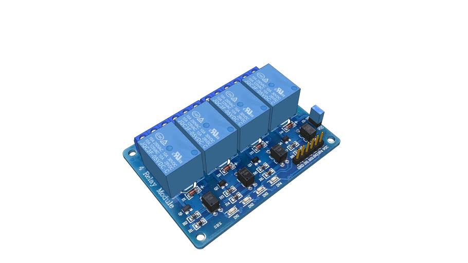
Relay Module Shield for Arduino ARM PIC AVR DSP Electronic 5V 4 Channel Relay.4 road 5V Relay Module
If you would like to support me:
patreon.com/wizzx
paypal.me/wizzx
bright thistle
fervent lance
Hello
i want to know the distance between each mounting hole of this 4 channel r...
Assuming the SketchUp is 1:1, download the file, open it with SketchUp, and use the measuring tool?
Or, you may adopt a solution dreaded by introverts: contact the manufacturer and ask!
limpid nest
junior gale
I will be keeping an eye out 👀
Looks like you can do as discussed
hidden night
Oh wow, I’m working on the worlds dumbest 65 key keyboard design and put together a macro pad as a starting point for that

I can share the KiCad files later if that’s helpful
junior gale
hidden night
I can share the KiCad files later if that’s helpful
The keyboard files?🤔
limpid nest
Can you panelize a design and then get a stencil for the panel before you break it up?
supple pollen
That's a common approach (you can see it in this AdaFruit manufacturing video: https://www.youtube.com/watch?v=KIZQfs9UsHE)
broken arrow
limpid nest
Can you panelize a design and then get a stencil for the panel before you break ...
Yes. I mean, the stencil is just your paste layer. so as long you pull that layer from your panelized board and not the subboard you should be good to go.
 fringe imp
What’s pcb?
unreal flax
"Printed Circuit Board", which is a standard type of board made from fiberglass layers and copper-foil wire traces.
fringe imp
Like if I wanted to design a macro keypad would I use this
Like how would I go about it
unreal flax
The tools are often called ECAD (electronics computer-aided design). The best free one is generally considered to be KiCad, so that's a decent place to start. The typical design flow is first to create your circuit schematic, which is a diagram showing what parts you use and what signals connect to each other. And then you work on the board layout, explicitly placing the chips in space and drawing the wires between them. Once you have that, you can send the files to a board fabrication house to get it made and optionally soldered with chips.
It's not "easy", but it is feasible to learn without going to university classes in electronics or anything like that.
distant raven
mind the uncorrected part name placing, but here's an nRF52811 board i'm working on

includes the illusive CP2102N-A02 QFN20
and the QFN32 nRF52811
big test will be how well my calculations for antenna filter play out
and fixed. probably a once over and i'll order this little gem

though, i think I need to put a pullup on the reset line.
yep, i do
 marsh nest
Alright PCB friends. I'm having an issue with my zenner diode setup.
Here's what I have:

The specific diode I have is: https://www.digikey.com/en/products/detail/onsemi/1N5225B/977560
The problem I'm having is that it's not clamping things to 3v. It's ending up at much lower voltages. Running the 5v from the source and shorting it out (as though the shutter button were pressed) gives me ~0.99v
If I go up to ~31v, well. The output is about 1.3v
unique patio
marsh nest
Alright PCB friends. I'm having an issue with my zenner diode setup.
Here's wha...
I think the current through the Zener is too low: https://electronics.stackexchange.com/questions/172484/zener-diode-voltage-too-low
1meg is not allowing much current
what about just using a voltage divider
marsh nest
unique patio
what about just using a voltage divider
I (theoretically) need to protect against surges of upwards of 300v
unique patio
i think something like an optoisolator would make more sense then
very short surges, like static?
you'll still want to protect to optoisolator from frying, but I guess the point is that the Shutter Sense is connected to something expensive
marsh nest
The original discussion on this went to optoisolators but the conclusion that I came to (Correct or otherwise) was that the isolators worked in reverse for what I needed - the high voltage was on the wrong side, basically
It's connected to an MCP23008, but. It's not intermittent surges. The idea is to control a camera flash, and some of the old ones can have really high voltages. So if I'm using one of those old flashes, well. It'll be happening a lot in potentially a fairly short period of time
unique patio
so it's that there might be HV on J2, which is supposed to be just open or shorted?
is Shutter Sense supposed to be pulled down when not triggered?
what input does SS expect?
marsh nest
Yeah, it's pulled down elsewhere (Or at least, it should be)
unique patio
with a common ground
marsh nest
The high voltage, when it appears, would appear on both pins of the flash/shutter button
Since the shutter button is what completes the circuit for said voltage
unique patio
so J1 is a common pushbutton, and J2 is supposed to be similar, but it might have junk?
common-mode HV?
marsh nest
J2 can be a flash (Triggered by said pushbutton) or can be a remote button
marsh nest
Yeah, and that is the biggest issue honestly. If it were only a flash output, I could get a double-pole button and never have to worry about it. And input, well. Also don't have to worry about it.
unique patio
i would say some kind of clamping component across J2, or two to ground at each terminal of J2, but I don't know if they would be fast enough
you could build some kind of detector across J2 to detect a short, which would short J1, but remove the direct connection to the rest of the circuit. AND use a double-pole button to short J2 when J1 is pressed
marsh nest
Sounds a little complex (For my knowledge at least) - and I already have the PCBs in hand.
unique patio
the detector could be maybe a HV MOSFET that is inverting?
ok, i am grasping at straws. I think, though that all the protection needs to be at J2, and you need to avoid connecting it directly to the rest of the circuit
marsh nest
I have legitimately no idea on how I would do that without making J2 not function as an input as well. My knowledge just isn't there.
I think I'm going to scrap the idea for high-voltage protection, honestly.
My other camera has a safe input range of... ~6v.
So to use any of those beefy flashes I'd need an adapter for that anyway
And if I'm working with 6v, then I should be able to do a voltage divider
unique patio
marsh nest
unique patio
<https://electrical.codidact.com/posts/280893>
Neat. I'll take a look and educate myself.
Still going to go for the easier (and known) solution, since honestly I don't forsee actually running into the issue - it'd just be neat to have.
unique patio
maybe you could just put an MOV across J2
answer says you need something faster than MOV, and suggest looking at how USB lines are protected
supple pollen
marsh nest
Sounds a little complex (For my knowledge at least) - and I already have the PCB...
Perhaps the low current TL431 variant I mentioned when I warned you about this?
marsh nest
supple pollen
Perhaps the low current TL431 variant I mentioned when I warned you about this?
Yeah, I don't think I fully understood what was going on (And... honestly still don't fully get it)
limpid nest
If I have a terminal block that's power OUT and I want to use diodes to prevent power in, do I use one on + and ground?
inland jungle
just on the +
limpid nest
What if they power it in reverse?
I assume there's a way to protect against that
I mean
I have reverse protection on the input, but idk what that looks like on the output
limpid nest
Eagle users, I made a connector footprint based entirely on the datasheet. Eagle is mad about pin holes being too close to the mounting hole. Do I just ignore it?
 void portal
guys, what is the most common smd power mosfet package?
I'm inclined to believe hsop8 is
unreal flax
limpid nest
Eagle users, I made a connector footprint based entirely on the datasheet. Eagle...
Possibly, although if the clearance rules are set based on your board house's parameters, the error might indicate that they won't be able to fabricate the PCB with holes that close together.
unreal flax
The default rules are just defaults, so may not reflect the actual manufacturing tolerances you'll see.
twilit mango
Eagle folks! I discovered a thing today that, for me anyway, is a total game changer. Originally the "Show" tool, when you click on a particular element, would highlight it a slightly different shade of green from the rest of the elements, making it super easy to miss things connected to it. If you go into the Options>Set... menu, and choose "High Contrast" in the Highlight section of the window, you can drag the slider around until it is a more obvious color to you. This color makes it obvious enough to see it when zoomed out to the whole schematic. Anyway, I'm excited about this discovery and figured I'd share. Might be old hat to many at this point.

 limpid nest
Neat trick kattni!
Eagle issue, library footprint has a bunch of text that doesn't have an anchor so I can't delete it and it's not obvious that it's in the footprint in the library
Thoughts?
 thick willow
What are some sensible MCD values for a 0603 or 0805 LED?
I don't want it blinding brigth that it is hard to read the silkscreen text next to the LED, but also not dim that its difficult to figure out if the LED is on or off under daylight
the LED light won't get diffused at all, it will illuminate directly into the retina
supple pollen
void portal
guys, what is the most common smd power mosfet package?
Dpak? Dpak2?
void portal
supple pollen
Dpak? Dpak2?
yes I also believe HSOP-8
supple pollen
I've seen a bunch of them in SOIC-8 too.
limpid nest
I finally used the sketch->PCB function in Fusion. It's pretty sweet tbh
 pure gorge
Is this wiring correct for the BNO085? And the I2C pins named "H_" are the ones I want to connect to my microcontroller right? (Also the capacitors I'm using aren't polarized, that's just the symbol I used)
 limpid nest
I know they aren't polarized, but it might prevent others from going "huh??" if you swapped the orientation of the cap connected to CAP
pure gorge
Ok, did that
limpid nest
do you have other I2C devices?
pure gorge
No this would be the only one
limpid nest
OK, even so, I'd just label BNO_SDA and BNO_SCL as SCL and SDA. It makes more sense since it's a shared bus
I am about to head out so I haven't opened the datasheet, so I can't say if any wiring is actually wrong, this is just what jumped out at me
pure gorge
Ok, will do
limpid nest
Also 2.2k feels a smidge low. It'll probably work fine, but I personally might go higher
distant raven
limpid nest
Also 2.2k feels a smidge low. It'll probably work fine, but I personally might g...
2.2K is pretty low
I prefer 4.7k-10k
 spice turtle
pure gorge
Is this wiring correct for the BNO085? And the I2C pins named "H_" are the ones ...
spice turtle
pure gorge
Is this wiring correct for the BNO085? And the I2C pins named "H_" are the ones ...
Im gonna be nitpicky about this but I would also edit the symbol and move PS0 and PS1 below the cap pin so you dont have that ugly cross wire. Turn C16 90degree's so it faces down as well. Just to make things look neater.
Based on the adafruit schematic, Id say yes
https://cdn-learn.adafruit.com/assets/assets/000/094/834/original/sensors_image.png?1600461991
 spice turtle
yes just missing the other connections
distant raven
this is going to be tight

improve the precision of placement and I can make it ever so slightly better lol

changed mask tolerance from 1mil around pads to 2mil and that seems to have made it slightly better

but dang this will be a small part
this will push the limits of the 6 layer service from OSHPark
probably even JLC
ember laurel
@distant raven what chip is that?
distant raven
nRF52811 WLCSP version
distant raven
There is technically a QFN32 but I wanted more board space for more features if I wanted
 thick willow
what is that BGa thing? some RF chip?
distant raven
Needless to say I have to be very tactful about soldering the part as i only bought 5
Yes, it’s the nRF52811
It is just 2.5mm x 2.5mm in size
Very small
thick willow
then what is the big one
distant raven
RP2040
thick willow
what can the rp2040 do that the nrf52 cant?
distant raven
nRF chip is for Bluetooth comms, it doesn’t have USB pins. RP2040 is the user friendly chip
thick willow
nrf are still quite capable, lot of ppl use them for much more than doing rf
distant raven
Oh sure, it is a cortex M4
But 24kB of RAM and 198kB of flash isn’t a lot
It’s made for super low power Bluetooth LE communication like HID and whatnot.
RP2040 has loads more RAM and FLASH
Plus circuitpython support
thick willow
nrf52840 has 256kB ram
distant raven
Sure, but RP2040 is far more accessible
thick willow
ok
distant raven
I like the nRF52840, it’s a great chip. I just wanted to use the RP2040 and still have BLE
thick willow
Is it safe to leave that copper above he antenna?
thick willow
ohh
distant raven
Yeah, probably not the most clear use of mask. I’d save a lot of space using a chip antenna
But BOM cost
thick willow
I wonder if clearing the sides ofthe antenna would have a a good impact
distant raven
🤷♂️
I technically don’t need the mask off of the antenna but I do it for the sake of testing
thick willow
The ESP32 recommends leaving space to the sides of the antenna
no i mean the copper no the mask
wher eyou got stitching
distant raven
I’m following a 2.48GHz trace antenna spec from TI for Bluetooth
They have a recommended keep out area that I mapped out. Will it perform well? No idea
thick willow
where you able to use the same stackup than the one recommended by TI
distant raven
Theirs was for 2-6 layer stack ups as long as keepout was consistent on all layers
Anyway, I’ll find out if it works through testing so cheers lol
distant raven
Nah, it was an older spec than that
thick willow
"The PIFA is placed on the edge of the motherboard PCB, as shown in Figure 6. The area around the
corner is kept copper-free, and any components such as the shielding that come close to the PIFA may
pull its frequency"
Anyway this antenna stuff has always looked like trian and error.. through some iterations you can always find what works best
distant raven
Oh sure, I don’t need amazing performance mostly just good enough
Chip antenna are usually the better way to go these days
But this is a prototype so I’m okay saving on BOM costs for now
This was the spec I followed
The keepout area on my trace antenna was designed to match the keepout they specify but it could be a bad design on my part to have copper there on the edge
Spec is from 2008 so it might not even really be very relevant anymore
distant raven
made some small adjustments. copper away from the sides, just on the bottom near the IC. Also realigned the mounting holes.

 viscid coral
Has anyone made the switch from EAGLE to KiCad recently? Autodesk's subscription model confusion is starting to get to me. I thought I had an education license and access to the full features, but that seemed to have ended without notice.
And EAGLE is now incorporated in Fusion 360. It almost seems like I can't access the full version of EAGLE within EAGLE as an independent software anymore. If I want to keep using EAGLE's full features, I have to do that within Fusion 360.
unreal flax
You should be able to still run Eagle as a separate app, though it uses the Fusion 360 license now.
(That is, a commercial Fusion 360 license gives you access to the Eagle Professional features.)
viscid coral
Gotcha. I can still run EAGLE as a separate app. The problem is I thought I had an educational license which would give me the full features of EAGLE. I think that's no longer the case.
I tried talking to a customer service rep, but they were unhelpful. Maybe I can ask again to see if the next person can help me out a bit better.
unreal flax
Yeah, I'm not sure how the education licenses work, I'm afraid.
I'm told that Altium gives free full licenses to anyone with an .edu email address too, if you wanted to get hooked on professional-level software you can't otherwise afford. 😉
viscid coral
Has Altium moved to the cloud-based system management as well?
unreal flax
The do have a cloud service, Altium365, but as far as I know it's still optional.
viscid coral
I'm kinda annoyed with the whole "renew every 6 months deal." I'm technically not a student anymore, but I do work at a university. I don't want my access being rejected after 4 years, assuming they put a cap on the number of times you can renew.
 unreal flax
KiCad is certainly a feasible option.
viscid coral
Yeah. After Autodesk bought EAGLE, I always felt that this change would be inevitable. So here goes. Thanks for chiming in though @unreal flax . I'll keep all these options in mind.
Which PCB design software do you use?
unreal flax
Personally I still use Eagle since I learned it a long time ago, and while I don't like what Autodesk has done with it, I also occasionally need a mechanical CAD tool, so that's justified keeping a Fusion 360 license for both.
I'm anticipating that the standalong Eagle version is not destined to be supported for much longer, and Fusion 360 doesn't run under Linux, so I'll eventually end up learning KiCad, I expect.
viscid coral
Yeah they're definitely ditching the standalone version of EAGLE pretty soon. I'm pretty sure they already stopped supporting it. There haven't been any updates for months. They still let people download the standalone version though.
 inner rampart
I'm making an SPI adapter board for the Feather. Hows it look ?
 thick willow
usea ground plane
i mean what you got will work just fine, but its a good practice to use ground planes
inner rampart
@thick willowthanks.
 weary fjord
I am new to discord! I wanted to say hi and see if anyone wanted to check a circuit, so I do not make any errors?
distant raven
Feel free to share what you’ve got and someone will usually be able to provide feedback
weary fjord
Thanks for any feedback.
 limpid nest
I think this might push me over the edge into kiCAD come the new year. They changed the size of the crosshair that shows the origin of schematic parts in Fusion. Can you guess which of these has the origin in it?
 supple pollen
weary fjord
Thanks for any feedback.
supple pollen
weary fjord
Thanks for any feedback.
That shows a symbol for a PNP bipolar transistor (which won't work) but a part number for an N-channel MOSFET (which might). The gate resistor is a little high, which is likely to cause slow turn-on and increased heat dissipation. You'll want a damper diode or snubber network to keep the flyback pulse from damaging the switching transistor. I don't see any provision to avoid saturating the inductor, which could damage it and the switching transistor.
weary fjord
supple pollen
That shows a symbol for a PNP bipolar transistor (which won't work) but a part n...
Yes, Sorry the Mosfet is an N-channel EasyEDA did not have that part but I will try to find a match.
What gate resistor value do you recommend?
Add a "NTE638" diode across Q1 thanks.
inland jungle
anyone have a favorite opamp for a cheap unity gain buffer?
supple pollen
TLV2462 is a handy low-voltage one. For generic use, I've moved from the old TL072 to the 5532, which is inexpensive and fairly versatile. However, it depends somewhat on the specs you're looking for (offset isn't usually a big deal in a buffer, but frequency, drive capability, and noise might be)
inland jungle
generally for going into an MCU ADC
supple pollen
That's normally not a very demanding job
inland jungle
yup, that's why I'm looking for cheap yet reliable options
supple pollen
I'd probably go for the NJM5532/NE5532/SA5532 in that case: it's been around a while, offered by several manufacturers, and has pretty decent specs. About half a buck to a buck in small quantities, and offers two op-amps in an 8-pin package. The ancient 741 is actually more expensive, and has worse specs.
inland jungle
thanks for the recommendation, added to my Mouser list
limpid nest
If you have to choose between a long trace across a +V plane or a GND plane, which do you choose?
I can't do a 4 layer
unreal flax
I expect it doesn't really matter. With just 2 layers, all the planes will probably be regularly interrupted by traces anyway in routing the signals around.
limpid nest
unreal flax
I expect it doesn't really matter. With just 2 layers, all the planes will proba...
Thanks
limpid nest
Does anyone have experience including a .STEP file into an EAGLE design? I assume it works the same in Fusion, and I'm about to start googling, but the Fusion EDA support is kind of lacking tbh
E.g I followed this https://www.youtube.com/watch?v=w7GFaCYed30&list=PLmA_xUT-8UlIh4hHJDCEDLPi3wQiMrPRY&index=5 tutorial and it just isn't working
inland jungle
@limpid nest I've imported STEP files into Eagle, it's not always straightforward
what steps are you having problems with?
limpid nest
I restarted fusion for unrelated reasons and it worked, >.<
 unreal flax
Shiny! What is that, clear soldermask with black FR4?
distant raven
Yeah
inner rampart
So I made this simple SPI adapter board for the Huzzah8266. It doesn't work for some reason and I can't figure out why. Is it possible the extra MOSI and CLK pins on the opposites of the board are different somehow because that's the only difference between when I wire it up manually (working) and using the adapter board (not working).

 distant raven
you should probably use 5 and 7 for SCK and MOSI respectively
since I believe those are mapped that way based on the ESP8266 module's SPI pins
inner rampart
@distant raventhose are 5 and 7, labels show IOnumber
distant raven
inner rampart
<@728676724522352733>those are 5 and 7, labels show IOnumber
Do you have boards without headers soldered?
inner rampart
@distant ravenyes
distant raven
inner rampart
<@728676724522352733>yes
Did you order this exactly? Or did you change it before ordering?
inner rampart
that's exactly it.
 inner rampart
yes i use those when manually wiring up but according to my multimeter they are physically connected to the other pins on the other side of the board so it really shouln't matter. I guess I should do a manual wire test with those other pins just to be sure . . .
inner rampart
nothing.
distant raven
Hmm
When you probe the pins on the headers you designated, do they show anything if you drive them high just as a digital output?
inner rampart
haven't tried that yet. just looking at the pcb layout now. looks like they are physically connected. WEIRD.
 inner rampart
If i figure this out I'll post it here.
distant raven
👍🏻
 inner rampart
So in KiCad if I import a board symbol (eg. generic feather board), the DRC complains that there is no board outline on the Edge.Cuts layer. How do I quickly assign the feather board outline to the edge.cuts layer of the parent PCB design ?
 gaunt cedar
inner rampart
So in KiCad if I import a board symbol (eg. generic feather board), the DRC comp...
gaunt cedar
inner rampart
So in KiCad if I import a board symbol (eg. generic feather board), the DRC comp...
it's likely that the outline on the edge cut isn't fully connected. sometimes on an import like that the poly lines are not exact. Can you hide all other layers except edge and zoom in and follow the path to make sure that's not the case?
inner rampart
@gaunt cedarthere is not an outline on the edge.cuts layer of the part to start with.
gaunt cedar
inner rampart
<@670084969003221014>there is not an outline on the edge.cuts layer of the part ...
can you link me the symbol you imported? I'm curious what's up.
inner rampart
I'm using the feather generic footprint from the KiCad 6.0

 somber marsh
Hi! I'm working on my first PCB, an rgb backlit mechanical keyboard with a detachable numpad that can be used as a calculator. I was somewhat set on using a kb2040 but an 8x10 key matrix uses all the available pins. I want to preserve the pins on the StemmaQT connector for the numpad. Is there any easy way with minimal extra hardware that allows me one extra pin for neopixels for the backlight? It seems excessive to use a different board (e.g. a feather) just for one more pin, but that's all I can think of at the moment. Is there any existing device to simply use neopixels over i2c? Thanks for any help!
My other option is to attach an extra pin to the numpad and just have it drive the neopixels. obviously not optimal, because the neopixels would stop working after the numpad is disconnected and I want it to be hot-pluggable. Without significant feature loss.
Just to save on complexity and pins, I used rotary encoder StemmaQT breakouts for any rotary encoders on the keyboard, and for a character lcd on the numpad, I used the i2c char lcd breakout. The StemmaQT port is very important to preserve for this! Thanks again for any ideas!
limpid nest
Hmmm so a gpio expander is out?
somber marsh
limpid nest
Hmmm so a gpio expander is out?
Not necessarily.. I'd need some help finding a suitable one.
limpid nest
You have a few options, let me re read over what you want to do with the pins
somber marsh
just an extra pin for neopixels. I dont even need pwm as I can swap another pin in as the one on the IO expander.
limpid nest
These are out of stock but an option maybe? https://www.adafruit.com/product/4991
Rotary encoders are soooo much fun! Twist em this way, then twist them that way. Unlike potentiometers, they go all the way around and often have little detents for tactile feedback. But, if ...
Cut down your pins used?
10 available on digikey
somber marsh
I'm alr using these! I've found all the i2c breakouts that are useful for this project
limpid nest
Ohhh
Ok
One sec
A 74hc595 should work
Oh wait
That requires pins
I'll find an i2c option
Are you looking to make your own board?
Or use mostly breakouts?
somber marsh
yep!
limpid nest
Ok because there's a great i2c expander that is large in breakout form but hard to find in chip form
It's a breeze to use but troublesome to acquire
MCP23008
If you can handle TH
somber marsh
So, In a previous version of my project i used the mcp23017 for the matrix itself, but I scrapped it due to stock concerns... It also feels a bit excessive for one extra pin... I think for the sake of my own sanity while programming this, I'd probably just switch to the feather before a large IO expander.
inland jungle
MCP23018 has pretty good availability in chip form
limpid nest
008 is smaller but yeah a feather might be in order. The aw9523 is perfect for you but it's so hard to get.
somber marsh
inland jungle
MCP23018 has pretty good availability in chip form
interesting...
somber marsh
limpid nest
008 is smaller but yeah a feather might be in order. The aw9523 is perfect for y...
A feather also affords me some comfort features, like traces on the pcb from the controller to some of the breakouts instead of using stemmaqt cables
Does anyone know what chip the I2C breakouts use or how they work? that might be an option, whatever it is. ex. https://www.adafruit.com/product/4991
Rotary encoders are soooo much fun! Twist em this way, then twist them that way. Unlike potentiometers, they go all the way around and often have little detents for tactile feedback. But, if ...
 somber marsh
yeah... that feather is lookin' mighty enticing...
inland jungle
the seesaw can breakout I2C into various functions, like rotary IO
unique patio
ATSAMD09 are now hard to get, and we are using ATTiny817 (we have a dev board for that)
for new designs, and maybe eventually for old designs
somber marsh
Using the castellated pads, the difference in footprint size isn't even that bad. I just have to buy an extra feather.

Thanks everyone!!!
limpid nest
Good luck!
 rancid lagoon
I'm building a project that uses a qt-py and a cusom pcb but i can't figure out how to get the footprint for a qt-py in kicad
somber marsh
do you have a footprint already?
gaunt cedar
inner rampart
I'm using the feather generic footprint from the KiCad 6.0
Here's what I would do. there may be a better way to do it but the outcome works.
After you add the footprint to the board press Ctrl-E to edit the footprint. On the right side hide all layers except the Front Courtyard. This poly line is broken up in segments so you'll need to work your way around clicking each section. Click a section and press E. you can change the layer the section is on - change it to Edge Cut.
Having the board courtyard and edgecut is kind of redundant so just moving it should be fine. You could always make a copy and move the copy to edge cut as well.
somber marsh
rancid lagoon
I'm building a project that uses a qt-py and a cusom pcb but i can't figure out ...
If you have a footprint already, go to Preferences>Manage Footprint Libraries... then click the small folder icon at the bottom of the list and select the folder containing the footprint.
If you need to make a footprint, first find the dimensions (I looked around a bit but found neither an existing footprint nor specific dimensions for the board) Then, in KiCad, go to Tools>Footprint Editor. Click the new footprint button at the top left, mark it as a through hole footprint, then add the pins according to the dimensions.
rancid lagoon
thx
inner rampart
@gaunt cedarthanks for the reply. Kind of tedious process but I guess that's I'll have to do.
 sweet inlet
I have a question and maybe someone here knows the answer...
I'm trying to ship electrical components internationally, some pcbs, some resistors/capacitors/usb connectors/etc -- basically a box of a bunch of parts.
Where can I find HS codes for customs? Is there a site that has common ones for electronics?
Basically handing off a project to someone else, so not charging for these parts, just need to get it to them...
gaunt cedar
sweet inlet
I have a question and maybe someone here knows the answer...
you can go to digikey and look up the part or similar and the bottom of the page will have HTSUS export classifications.
sweet inlet
gaunt cedar
you can go to digikey and look up the part or similar and the bottom of the page...
Amazing! Thank you!
 broken python
I'm considering designing a PCB for a project, would probably order about a dozen, in the continental USA, and it would need to be dual-layer, probably about the size of a business card.
What would be some recommended vendors for this low-volume? Or am I better off just using solderable breadboards?
unreal flax
Do you need just bare PCBs or fully assembled?
broken python
unreal flax
Do you need just bare PCBs or fully assembled?
I would need the holes drilled and the solder pads exposed, but no components actually mounted through the holes
just trying to make it a little bit easier than making a bunch of jumper wires around a solderable breadboard
cleaner with fewer points of failure, not necessarily easier
unreal flax
I'd start at https://pcbshopper.com/ to compare some common options. That sort of board is a very commodity need, but the "in the continental USA" will restrict you, maybe more than you really need.

PCBShopper is a price comparison site for printed circuit boards. Enter your PCB's specs and immediately see prices from more than 20 PCB manufacturers.
broken python
unreal flax
I'd start at https://pcbshopper.com/ to compare some common options. That sort o...
Rereading my original post I was potentially unclear - I don't care the origin, but I need them to be able to ship to me, and I am in the continental USA/"lower 48"
Thanks for the link!
gaunt cedar
here's an option if you don't mind red https://www.digikey.com/en/resources/dkred
unreal flax
broken python
Rereading my original post I was potentially unclear - I don't care the origin, ...
Ah, gotcha, that should open things way up, then. Lots of cheap overseas options that ship to the US.
inland jungle
oshpark is pretty reasonable for small boards, low qty
distant raven
Yeah, a feather sized board for 3x costs around $9
For 2 layer
Get free shipping through the post office
JLC would be $2-5 for 2 layer, probably $14-$19 for shipping DHL
limpid nest
you do get 5 boards though, tbf
distant raven
Yeah, shipping is just a killer
distant raven
It makes more sense when you’re ordering 500 boards at a time or massive panels
I usually just do OshPark for prototypes
limpid nest
I make pi sized boards, it makes sense there too
distant raven
This board for instance

$24 for 3, $8 a board but free shipping lol
Plus I only need to validate on one PCB before the final feather 🙂
limpid nest
I'm currently working on a board for testing stuff. I'll have to see if it make more sense to go thru JLC
broken python
Think I'm gonna go with just solderable breadboards after looking at prices, but if I can't find a serial adapter like I described in #general-tech , I might have to get custom PCBs made to build my own serial adapter!
distant raven
broken python
Think I'm gonna go with just solderable breadboards after looking at prices, but...
Making your own PCBs is like owning a boat or a hobby car. Super rewarding and not something you tell your significant other about the cost of lol
broken python
distant raven
Making your own PCBs is like owning a boat or a hobby car. Super rewarding and n...
I figure if I'm gonna do it, I might as well make something too advanced for basic breadboarding
distant raven
Great idea 🙂
broken python
(again, after seeing prices. If they were $5/each in my hand within a week, I'd have custom PCBs for my current project, too)
 finite meteor
👋 what's the easiest way to prototype with a pcb that doesn't have headers installed when you don't want to add solder to it? Is there a temporary way to form connections? I've found this DIY clip-on connector but was wondering if there's something more off-the-shelf https://www.instructables.com/Pogo-Pin-Programming-Connector/

Instructables
Pogo Pin Programming Connector: Pogo pins are spring-loaded conductive pins that are good for making temporary electrical connections. They are often used for testing electrical signals on printed circuit boards.I recently had a project where I needed to make 400 identical circuit…
unreal flax
If it has holes or pins, mini hook clips are a good option.
finite meteor
unreal flax
If it has holes or pins, mini hook clips are a good option.
So for example with this, you could use the mini hook clips?
 unreal flax
At least on the board-edge row. The interior row would be more difficult.
supple pollen
finite meteor
👋 what's the easiest way to prototype with a pcb that doesn't have headers inst...
I had bought a ready-made one from China, but now they're available from AdaFruit: https://www.adafruit.com/product/5433

The Pogo Pin Probe Clip with 6 pins in a 2.54 / 0.1" pitch spacing is a great way to test and connect with pin-point accuracy without soldering! It's sort of like an ...
limpid nest
Do they make pumps that are like well pump size and larger that can be controlled by PWM? Speed control?
I'm having trouble finding it
 minor axle
limpid nest
Do they make pumps that are like well pump size and larger that can be controlle...
minor axle
limpid nest
Do they make pumps that are like well pump size and larger that can be controlle...
What sort of pump are you looking for?
limpid nest
Large pump, multiple gallons per minute, submersible is nice but not needed
10ish feet litt
Lift
minor axle
I mean afaik most DC pumps are just DC motors hooked up in fancy ways so you ought to be able to just PWM it
inland jungle
that size pump might be mains AC
minor axle
Oh yeah I don't think you can PWM AC very easily
 knotty tiger
there are variable frequency drives (VFDs) that are made for running AC induction motors at different speeds. they're not cheap, from what i recall (and might not work on a single-phase motor)
inland jungle
you can use a diac/triac to get a variable 'turn-on' delay for each 60Hz cycle, but I have no idea what that would do to a motor
essentially a 'dimmer' circuit
minor axle
FWIW, we should move this discussion to #help-with-projects
 candid axle
Would anyone happen to know where I can find the relevant KiCad symbol and footprints for this Adafruit part? https://www.adafruit.com/product/4421

This is a screen for advanced hackers who like the look of the TFT screen we've put into the TFT Gizmo and Monster M4sk. The 1.54" display has 240x240 16-bit full color pixels and ...
ember laurel
distant raven
This board for instance
Who. Soldered. That.
ember laurel
I was gonna ask if it was Michael J Fox


 ember laurel
🙂
distant raven
i slathered paste on the pads and hoped for the best
I'm cheap and don't buy stencils if it's not a final product lol
ember laurel
oh paste
I just solder such stuff without paste, just use wire
KiCad question: Is there a way to change multiple vias at once to be buried/blind?

this dialog isn't very helpful for that
distant raven
ember laurel
I just solder such stuff without paste, just use wire
i don't have thin wire solder lol...
ember laurel
I'm testing out my first project in KiCad
and I installed this Via Stitching plugin
but it generates normal vias - and I prefer my vias to be blind/buried, unless they have any other purpose than ground sandwich stitching
ok - I got it
issue was that they were grouped, and I had to enter group, then press 'E', and it changed all.
I start liking KiCad though, really not too shabby.
quite a lot simpler than Altium, which I'm used to.

Made this little board today, just about ready to order it.
ember laurel
I don't find myself missing that much
I find the schematics editor better really.
I miss the property list stuff from Altium
windows where you can browse and filter parts and so on
and also some routing related things.
but for a free package, this is excellent
rancid lagoon
distant raven
I need to try KiCAD one of these days
if you use eagle you can import both symbol/footprint librarys and projects in kicad 6
distant raven
i'm aware, i just need to take the time to do it lol..
rancid lagoon
one thing that took me a while to discover is if you need to edit a footprint in a eagle library use "save as" to convert it into kicad format then save it
unique patio
This channel has been renamed to #help-with-hw-design to broaden its scope a bit. The description is now: This channel is for help in sourcing parts, and hardware and PCB design.
limpid nest
In that mind I'm going to move my question here
Is adafruit product 9 strong enough to be sensed thru some 5/8 plywood?
unreal flax
Yes, almost certainly... wood doesn't have much effect on magnetic fields, so it would just be the same as detecting it through the same distance in air.
 glacial gale
i really want to make a gpu, are there any things i should look out for?
unreal flax
glacial gale
i really want to make a gpu, are there any things i should look out for?
Define "make"...
glacial gale
write a soft version in chisel3/vhdl to try out on an FPGA
unreal flax
I guess the main thing I'd suggest is to go back in time and start simple. That is, instead of trying to replicate a modern NVidia GPU, which is quite fantastically complicated, target the sort of graphics accelerators used in early home computers and handheld gaming consoles, which had things like sprite engines, scrolling backgrounds, etc.
glacial gale
unreal flax
I guess the main thing I'd suggest is to go back in time and start simple. That ...
you think something like the geforce 256 (1999) would be a good start? or maybe a bit earlier
unreal flax
Yeah, I was thinking more like the GameBoy (1989), heh heh, but you can calibrate things to your skill level in FPGA coding.
spice turtle
unreal flax
I guess the main thing I'd suggest is to go back in time and start simple. That ...
Maybe off topic but isnt it amazing how engineering GPUs is basically just built on the shoulders of giants? I just wonder how vastly complicated a GPU has become and yet, a human or group of humans made it. Its a recursive design that seems to get better as new tech comes out.
And yet here we are, doing 8 bit or 32 bit stuff
glacial gale
heheh it is prob the most complex thing humanity has ever made
 gray lance
beginner question: I want to add a switch to the mains side of a power supply. Do i add it to the hot? Neutral? does it depend on the PS?
add it inline*
spice turtle
Hot side.
Use insulated crimp connectors OR when you solder, be sure to use heat shrink to protect the wires
rancid lagoon
gray lance
beginner question: I want to add a switch to the mains side of a power supply. D...
No it does not depend on the power supply. Always put the switch on the hot side no mater what the supply is
 safe panther
I'm trying to hook up a raspberry pi pico to a tp4056 charger/battery like this diagram/explaination, but I'm concerned about trying to find a suitable P-FET


it mentions above as well "An example of a suitable P-MOSFET for most situations is Diodes DMG2305UX which has a maximum Vt of 0.9V and
Ron of 100mΩ (at 2.5V Vgs)." But I can only find suitable P-FETs with a Vt of 2 volts at the lowest... from what I understand that feels like a bad idea for this arrangement?
or am I overworried/overthinking
If a P-FET with a Vt of 2 would still be safe/work but just less efficient I wouldnt mind that either, my main concern is avoiding any problems/smoke with the battery stuff while also being able to optionally power the pico's USB port with the TP4056's input voltage
supple pollen
safe panther
it mentions above as well "An example of a suitable P-MOSFET for most situations...
It may or may not be. The way to find out is to look at the datasheets for the parts you're considering and see what the Ron is for the parts in question at a gate voltage equivalent to your charger output (possibly subtracting Vbus if it's likely to be non-zero for the situations that apply). Several AdaFruit designs use P-MOSFETs in a similar configuration, you could see which parts they use.
safe panther
Hm reading more of this section of the pico docs, I might be fine with just a diode anyway if I don't care too hard about efficiency
If I never read this section at all I would have naively just hooked up the OUT of the TP4056 charger to VSYS on the pico... thats fine as long as nothing gets plugged into VBUS supplying power. I thought harder about this because i'm also gonna need situations where the pico is power OUT of vbus, which I could only really do by linking the vIN and vBUS (I want a keyboard plugged into the pico's USB port powered by the USB port of the TP4056, the keyboard doesn't need to function when running off of battery power though)
But I think a simple diode will do the same job as that p-mosfet less efficiently and I'm mostly going based off whatever I have around/can find fast rn
if I can find a decent diode since a 1v drop from the battery might not be too great
supple pollen
Schottky diodes are popular for this duty, as they have a low voltage drop. It's a popular approach.
safe panther
yeah that was mentioned before the pfet solution i kinda just lost the mark a bit
spice turtle
Does anyone know how to calculate the power dissipation of a TRIAC?
rancid lagoon
measure the voltage drop across the triac then multiply it by the flowing current in amps then the output is the heat generated in watts
spice turtle
I actually found it a little after your reply. Its a little more nuanced than that 😅
https://www.farnell.com/datasheets/1760767.pdf
AN10384 by Philips
limpid nest
That is a bit more complex
spice turtle
Im glad they give examples there atleast
limpid nest
Some datasheets are really nice
distant raven
Others like those for chip antenna are… sparingly detailed
limpid nest
Or spec sheets for motors sometimes
rancid lagoon
rancid lagoon
measure the voltage drop across the triac then multiply it by the flowing curren...
At the time that seemed accurate but now that i think about it i can see why it’s not accurate
 verbal echo
Hi there, could someone help me understand a diode's capacitance as mentioned in the datasheet? And additionally know if RRT has any effect on 0-3.3v and 0-5v DC signals.
I'm trying to understand a circuit+code that behaves OK at 16MHz, but goes bananas at 125MHz (same operations). I believe it's the diodes, as a friend that was having the same problem replaced the unknown spec diodes with new diodes of known spec 1N4148 and his problems went away. I want to try to understand what factors come into play, and I don't have an oscilloscope+function generator to try to observe more/better the isolated behavior of the diodes I have.
supple pollen
Capacitance conduct AC signals, the higher the frequency, the more they conduct. So high frequency signals can leak through high capacitance diodes in the reverse direction.
Similarly, long recovery time can allow more of a high frequency signal to get through before a diode shuts off
verbal echo
@supple pollen ok, but I imagine the signals I'm working with are more like a DC square wave zero to logic high, since it's basically driving output pins high, reading, then setting low to go do those steps on a different pin.
Is the diode acting as a capacitor in parallel? im I correct to imagine it as holding the anode side at a higher voltage after the pin connected to it is set from high to low?
or does it hold the cathode side high for a little while? I tried to reproduce this in an online circuit simulator but was not able to get a diode to misbehave using only a source clock, a diode and ground. So I want to at least enumerate which underlying concepts I'm missing
knotty tiger
a square wave isn't DC
or to put it a bit more verbosely, a square wave might look like piecewise DC, but it actually contains (in the ideal case) an infinite frequency spectrum
knotty tiger
verbal echo
or does it hold the cathode side high for a little while? I tried to reproduce t...
what online circuit simulator are you using? if it's only simulating ideal diodes, that might be part of your problem
supple pollen
Yes, it does basically act like a capacitor in parallel with the diode
verbal echo
supple pollen
Yes, it does basically act like a capacitor in parallel with the diode
ok, so at the instant I set the pin that is connected to the anode (output pin) to low, voltage on the cathode will go low sharply, and the anode will remain high and dissipate power through adjacent lines to it?
@knotty tiger I don't remember, it was the first result when I googled, it had 1n4148 and 1n40something-something... but I think I was not able to get those to misbehave at frequencies it was able to plot/graph in a meaningful way
knotty tiger
verbal echo
ok, so at the instant I set the pin that is connected to the anode (output pin) ...
this reads a bit like a non sequitur to me. maybe you would like to post a circuit diagram, or describe in more detail how this is hooked up? like what kind of microcontroller(?), which pins, whether you're setting the pins as input or output (with or without pullup)
verbal echo
nos-sequitur is a bit harsh, I'm just trying to explain how I'm visualizing a capacitor in parallel to the diode. If that doesn't logically follow the previous statement, calling it out in this manner is not constructive.
The reason I'm approaching the subject in this manner is precisely to not get distracted with x or y microcontroller, or pins, among other implementation details and focus on the one small piece of the puzzle I want to understand in isolation.
knotty tiger
i think you're omitting enough details that i'm having trouble telling what you're observing, versus what you're interpreting
verbal echo
that is my interpretation and I'm asking if my mental model is correct after being told what I understood as "the capacitance in the datasheet is as if there was a capacitor in parallel to the diode at high frequencies"
knotty tiger
closest i can find to a circuit diagram of a simplified model of diode capacitance is https://uweb.engr.arizona.edu/~brew/ece304spr07/Pdf/Diode Capacitances.pdf
knotty tiger
knotty tiger
closest i can find to a circuit diagram of a simplified model of diode capacitan...
(i think you want to put an ideal diode in seriesparallel with that for a more complete model?)
verbal echo
I just want to know, what is that thing on the datasheet and how does it behave? how do I visualize it?
this about two parameters, rrt and capacitance for diodes.
I give context on why I am asking the question and it is a thing I am observing and don't understand. But that problem nor the observations are what I'm asking.
What I expect to find are pointers to graphs, or simulations, or an explanation of how these things behave and what things influence those behaviors.
verbal echo
knotty tiger
closest i can find to a circuit diagram of a simplified model of diode capacitan...
thank you for the link, let me check that model out, can you explain what you mean by an ideal diode in parallel? do you mean to the first diagram?