#help-with-hw-design
1 messages · Page 64 of 1
 supple pollen
 limpid nest
hmm I was including adafruit ha, classic misstep
Seems like something that should be corrected in the official adafruit.lbr, given how much they use the 4 pin SH connector
supple pollen
I use the AdaFruit, SparkFun, and MicroBuilder libraries when I can, but otherwise I roll my own (bodger.lbr) or start looking for other possibilities
limpid nest
I couldn't find microbuilder online except from weird sources
supple pollen
You could, of course, grab the Eagle files for a board with it and extract the part definition from there.
supple pollen
I haven't tried in Fusion, I'm stuck on old Eagle 7.7 since they stopped updating the licensed version.
supple pollen
I guess you could grab an old Eagle version, use it to extract the library, then import that, but it's likely more trouble than it's worth.
limpid nest
Yeah
Easier to make my own
The really annoying thing about Fusion? Every. Single. Google. Search about it ends up with results for the 3D modeling side.
supple pollen
The first four hits I got were all for Eagle
limpid nest
If you search for Fusion specifically
You can add a bunch of search terms to get it to work but it's annoying
supple pollen
Ah, I (intentionally) didn't search for fusion.
 fervent lance
my ex-uni pcb business use altium and you have to export it using a specific dialogue with 7 windows for them...
so basically 5k$ for one pcb before you even make one...
 cosmic plaza
Hi folks, can I get some design review feedback on this:
https://oshwlab.com/logan.p.herrera/tuning-fork-audio-amplifier_copy
In EasyEDA open source hardware lab, open source square pools all kinds of electrical design engineerings together to realize resource sharing easily.
Next step is JLCPCB fab + assembly
one style question: is there a convention for signals that leave the sheet in a flat design like this?
cosmic plaza
Also I built and characterized a 4th order filter (linked is 8th) to validate the TI calculator. Turns out it really works! Though with more peaking than expected. I think it's to do with the extra DC blocking cap + filter input impedance

 heavy jasper
I’ll try to take a look tomorrow evening!
cosmic plaza
Thanks @heavy jasper !
 pure gorge
Im trying to use an MCP23016 I2C expander in a schematic, but I cant tell if I need to use the INT/interrupt pin. In the past I've had to solder I2C connections with an INT pin but is it safe to leave it floating?
 worldly schooner
pure gorge
Im trying to use an MCP23016 I2C expander in a schematic, but I cant tell if I n...
worldly schooner
pure gorge
Im trying to use an MCP23016 I2C expander in a schematic, but I cant tell if I n...
The INT pin is an output from the MCP230xx to your MCU. It should be fine to leave it floating.
pure gorge
Ok, thanks
Hopefully I dont fry anything and waste a board purchase, this is my first board
 distant raven
do you think it's permissible to use a 100nF ceramic in place of a 10nF ceramic if it's just used between a reset line and gnd?
i know it'll affect timing of the reset line but i'm not sure if it's enough to make a huge difference where it would negatively affect operation
heavy jasper
If there’s a switch on that reset line and you don’t have some series current limiting resistor going into the switch, make sure the added capacitance isn’t more likely to weld your switch contacts over time.
(In general the series current-limiting resistor helps prevent that regardless of cap size)
distant raven
heavy jasper
If there’s a switch on that reset line and you don’t have some series current li...
it has a 10k pull up if that helps clarify
heavy jasper
Not so much worried about the 10K pull-up, but say you have a huge cap charged to 3.3V, then you short that cap to ground via a reset switch. The cap will have a spike of current out into the switch that I’ve (rarely) seen fuse tiny switches before.
If you don’t have a manual reset switch (or anything else pulling the line low) and just have the 10K pull-up, then it seems pretty reasonable.
distant raven
heavy jasper
If you don’t have a manual reset switch (or anything else pulling the line low) ...
It’s this board in question

Reset button on the line for manual reset
Reset traverses between two IC
 bright thistle
Hello!
distant raven
Hi
bright thistle
I have a bunch of buttons individually connected to gpio, what alternatives would you suggest in order to reduce the number of wires going to the Pi (I2C, USB, SPI...)? :)
I want to try designing a suitable PCB, but don't really know which method I should use 😅
limpid nest
There are a bunch of SPI and I2C GPIO expanders. But you'll have to have the traces for the buttons somewhere
bright thistle
limpid nest
There are a bunch of SPI and I2C GPIO expanders. But you'll have to have the tra...
I think I could use the I/Os from my boards where the buttons are collected, then :)
fervent lance
I've used 3-to-8 decoders in small projects.
 alpine slate
Hey guys! How "hard" is it to learn PCB design? I need a PCB with really only a place to solder a rpi PICO on and a bunch of LEDs connected to itl
limpid nest
It depends on your goal and needs. That doesn't sound terribly tough
Check out kiCad for a free software that's basically enterprise grade
alpine slate
limpid nest
It depends on your goal and needs. That doesn't sound terribly tough
Really just a bunch of LEDS that are placed in a specfic manner
alpine slate
limpid nest
Check out kiCad for a free software that's basically enterprise grade
thanks!
limpid nest
How are you sourcing and sinking the current?
alpine slate
limpid nest
How are you sourcing and sinking the current?
ngl i have no idea how all this works im pretty new to this
limpid nest
Hmm OK, just thought I'd mention that it's not really usually feasible to power "a bunch" of LEDs from a microcontroller directly. A small number is possible, but also not recommended.
alpine slate
im talking about these small leds btw
 limpid nest
Yeah, it's still not usually best done. There are ways to do it though, LED driver chips are not hard to find
 tough matrix
typically, you can use 1 pin to source or sink power to 1, maybe 2 LEDs
if you need to power 10 LEDs, you do need an led driver, or maybe just a mosfet
limpid nest
Yeah LED driver is the "right" way to do it, but you can get away with a Mosfet without much trouble if you just need to blink N LEDs and have them be all on or off at the same time.
 modest grail
i have a board i made a mistake on and im trying to rerout the trace. what do i use to seal it and bond it to the board?nail polish? kapton tape?
distant raven
modest grail
i have a board i made a mistake on and im trying to rerout the trace. what do i ...
You could. Make sure to trim the bad area
modest grail
I already cut the old traces and verified they wer cut with a multi
distant raven
Kapton tape should be sufficient then
modest grail
How about for a more perminate fix
limpid nest
How sturdy and/or long term are screw terminals?
worldly schooner
With ferrules? Very.
Industrial installations within a proper cabinet stay functional for decades if done right.
 steel valve
What solder paste should I use for hotplate soldering? I am soldering small components onto a 15x30mm pcb
distant raven
What kind of application is the board?
steel valve
distant raven
What kind of application is the board?
The board intends to be a breakout for a sparkfun artemis bluetooth module
distant raven
Okay, you’re probably okay using low temp
distant raven
It will be like Bismuth, Tin, and Copper usually
steel valve
Where would I buy that paste at
steel valve
What's the name of the paste you use
steel valve
Do they have paste jar versions?
I am going to use a stencil
w/ a squeegee to put the paste on the board
steel valve

Description Solder Paste in jar 50g (T3) Sn63/Pb37 no clean 90.25% metal. Alloy: Sn63/Pb37 Flux Type: Synthetic No-Clean Flux Classification: REL0 Metal Content: 90.25% metal by weight. Particle Size: T3 (25-45 microns) Melting Point: 183C (361F) Size: 50g jar Shelf Life Refrigerated >12 months, ...
Is this it?
distant raven
Chip Quik NC191LT50 Smooth Flow Low Temp Solder Paste Sn42/Bi57.6/Ag0.4 T4 50g Jar https://www.amazon.com/dp/B08KWLLFT4/ref=cm_sw_r_cp_api_i_C2VZWYP18QBFQKA65HXJ

Smooth FlowTM Technology Developed with a lower density flux vehicle for better shear spread and improved flow during heating Halogen Free (EN14582 test method) Specifications Alloy: Sn42/Bi57.6/Ag0.4 Flux Type: Synthetic No-Clean Flux Classification: ROL0 Metal Content: 89.75% metal by weight. P...
I recommend lead free if you’re not sending things to space
steel valve
What's using lead free solder do differently
distant raven
Well, it doesn’t have lead in it which is better in general
Low temp melts even lower than leaded solder
The only real reason to use leaded solder anymore is in space application
steel valve
Ok just making sure cause the surface finish of my PCB is HASL (With Lead) from JLCPCB
distant raven
Oh gotcha
steel valve
Since at that point there would already be lead involved
distant raven
Yeah, if there’s already lead it wouldn’t hurt to use lead
steel valve
Ok so https://www.amazon.com/Solder-Paste-Sn63-Pb37-clean/dp/B07BH5LP5G/ref=sr_1_6?crid=1XGJI6WJHMKEI&keywords=solder+paste&qid=1651287378&sprefix=solder+past%2Caps%2C158&sr=8-6 would work then
Description Solder Paste in jar 50g (T3) Sn63/Pb37 no clean 90.25% metal. Alloy: Sn63/Pb37 Flux Type: Synthetic No-Clean Flux Classification: REL0 Metal Content: 90.25% metal by weight. Particle Size: T3 (25-45 microns) Melting Point: 183C (361F) Size: 50g jar Shelf Life Refrigerated >12 months, ...
Cool
distant raven
Yeah
distant raven
Hot air gun to help with heating the top
distant raven
Masking tape and usually spare PCBs
alpine slate
limpid nest
Yeah LED driver is the "right" way to do it, but you can get away with a Mosfet ...
Okay I just checked and i need round 50-60 SMD Leds or maybe even more. Is this achievable? Each need to be accessed individually
limpid nest
Just FYi, that's a good amount of power
Off the top of my head, you could probably do it with the AW9523 chip. But actually getting those chips and then soldering them isn't easy
With multiple of that chip
Each one can do 16 LEDs
You can have up to 4 before you need a multiplexer
So 64 LEDs
alpine slate
okay maybe ill take my 2nd config then lol
limpid nest
You CAN get the chips
It's just not easy and the process of soldering them is harder
But it would be the most compact way to do it.
They are tiny tiny

That's my pinky finger
alpine slate
oh yeah thats tiny
alpine slate
but i also wouldnt be able to power them by usb would i lol
limpid nest
You'd struggle to power 60 LEDs over USB except at very low brightness
Over computer USB that is
alpine slate
they wont be all on at the same time btw
limpid nest
Hm well that would change things
alpine slate
limpid nest
Hm well that would change things
how many of them would you expect to work at the same time via computer usb?
limpid nest
Are you using a particular devboard?
alpine slate
limpid nest
Are you using a particular devboard?
pi pico
limpid nest
ok, so that takes ~85-93mA, we'll go with 100 mA to be safe. So you have about 400 mA for LEDs and LED drivers
alpine slate
okay thank you!
 fallen pulsar
has anyone tried to use crystal-less usb using an stm32 and stm32cube? I can't for the life of me figure out how configure it properly
im using a stm32L433rb
 upper moss
Hi all! On an MCU board where there is enough room, what is the preferred STEMMA I2C connector? Regular? Or is everything moving to STEMMA QT? As I read the docs, it says that QT is being used to keep sensor boards small. But I also heard that everything is moving to QT....
distant raven
most of all the newer Adafruit boards are moving towards STEMMA QT
upper moss
distant raven
most of all the newer Adafruit boards are moving towards STEMMA QT
thanks for some feedback! I was thinking of going that way but appreciate any input!
limpid nest
The biggest downside i see of stemma QT is you can't pump as much power down the lines.
But it's not meant to be a power transfer method
 elder peak
Yah, often times you don't necessarily want to even use the same power rail either.
Like, either it's a sensor with low power requirements or it's something like my LED driver boards where you might be driving it with a completely separate power supply.
supple pollen
alpine slate
Okay I just checked and i need round 50-60 SMD Leds or maybe even more. Is this ...
It might be easier to use a multiplexed chip (or charlieplexed for even more LEDs, but more confusing wiring)
limpid nest
Oh yeah I forgot to mention that my method gives you dimming, which is one of the big advantages alongside pcb size. There are other options
pure gorge
What should the L1 inductor be on the first page if im using a single cell lithium battery? https://www.ti.com/lit/ds/symlink/tps61322.pdf?HQS=dis-dk-null-digikeymode-dsf-pf-null-wwe&ts=1651376981641
 unreal flax
pure gorge
What should the L1 inductor be on the first page if im using a single cell lithi...
unreal flax
pure gorge
What should the L1 inductor be on the first page if im using a single cell lithi...
Have a look at section: 9.2.1.2.3 Inductor Selection.
pure gorge
Oh, I didnt know there was a section about it. Thanks
 warped atlas
VFD Question for y’all: I intend to make a project that uses 8 of these tubes

Each one has a filament, which must be driven with 2.2V AC (in the kilohertz, exact freq doesn’t really matter)
I intend to achieve this w/ a 555 + transformer
would I have to power EACH filament with its own mini transformer circuit, or could I just wire them all in parallel?
 inland jungle
how much current do you need to drive them
supple pollen
Parallel should be feasible
heavy jasper
@cosmic plaza I'm not sure how to check stuff/no-stuff in EasyEDA, but e.g. it seems like you have R1 and R8 in parallel with both stuffed. The comparators are mostly about just having a variety of options by the looks of it, but I'm not sure that the COMPA one (that just compares INA directly) will be super useful for the phototransisor models, given that both the pullup voltage and the comparator reference voltage is 2.5V (so the phototransistor outputs will either be decidedly less than reference, or right around reference in a Voffset-sets-output kind of way).
It looks like you're using a micro-USB connector, I'll make my standard pitch for a type-C version instead (especially if you're already getting this board professionally assembled or are willing to do hot-air work, given your choice of BGA microphone)
For the type-C version, if LCSC sells the power-only type-C connector that could work and be easier to solder
22uF is also kind of a bunch of capacitance directly on a USB output - it's probably okay - especially if you're just plugging into a power brick instead of a laptop - but if you had a laptop that was particularly stringent about inrush / current-limiting specs (coughmacbookcough) then you might run into some problems.
cosmic plaza
Thanks @heavy jasper
all components are stuffed
the R1 and R8 combo is because the microphone output impedance is very nearly the required resistance for the first stage filter
so it gives some flexibility in prototyping microphone present (remove 270 ohm) vs signal generator present (remove 0 ohm)
however the phototransistors have other impedances
and the filter response is already looking sensitive to precise input impedance 🤔
cosmic plaza
heavy jasper
22uF is also kind of a bunch of capacitance directly on a USB output - it's *pro...
what level of capacitance is obviously fine? or is it "none unless active inrush limiting is present"
heavy jasper
I’m actually not sure - but I knew of a case where 10uF of ceramic was too much.
cosmic plaza
In layout, 5V and 2.5V are distributed in a power layer (Inner 2)
all mixed up and interdigitated
with 1 mm tracks
above continuous GND plane
does anything about that layout look concerning?
pure gorge
What should be used to give the backlight 19v on this display? Seems kinda high for an LED https://www.orientdisplay.com/wp-content/uploads/2021/10/AFK320480A0-3.5INTM-spec.pdf
worldly schooner
pure gorge
What should be used to give the backlight 19v on this display? Seems kinda high ...
Generally, these type of display backlights are driven by current sources. You can reference https://learn.adafruit.com/assets/24414 from Adafruit's DPI TFT Kippah (2454) for what they use for such displays.
 slow plover
I think the RP2040 is neat, and it's cheap enough for me as a hobbyist to consider designing boards that use it directly. As a non-EE who's largely self-taught, but able to understand most of the concepts involved re: high-frequency signals, am I likely to have much success trying to adapt the reference design for a specific application?
It seems to me that most of the difficulty is likely to be from RP to flash, USB, and crystal
from what I understand, it's mostly a matter of ensuring proper impedance/timing?
worldly schooner
slow plover
I think the RP2040 is neat, and it's cheap enough for me as a hobbyist to consid...
If I'm being totally honest, the hardest part is probably not even impedance/timing, as the signals from the RP2040 are still considered low-speed and the impedance should be fairly tolerant thanks to its series resistors. Right now, the two hardest parts are going to be 1) selecting and sourcing materials, as the exact parts on the reference design might not be in stock at the time of this writing, and 2) debugging your board after it comes back from fab, because even the most experienced engineer will need a couple of bodge wires and a second spin to make sure everything is perfect.
That being said, if you've never designed a board before, it may be easier to start with using a surface-mount Pi Pico (or QtPy) in place of the RP2040, as all the necessary circuitry is already there for you. That will save you the headaches of dealing with the crystal and power supply circuitry, and save you a lot of time in terms of a complete design. From there, integrating an RP2040 is much simpler, and it narrows the areas of potential failure to the passives and components directly attached to the RP2040 chip.
distant raven
It’s actually pretty easy all things considered
Tons of designs that you can easily reference for your own board.
But the USB peripheral is probably the least spectacular part of the RP2040 other than the load of capacitors you need for all the inputs
USB PHY1.1 is pretty slow considering plenty of micros have USB PHY 2.0
worldly schooner
distant raven
USB PHY1.1 is pretty slow considering plenty of micros have USB PHY 2.0
In its defense, having a lower-speed USB peripheral makes designing custom boards far easier, especially for new PCB designers?
distant raven
But the Pico is a much better deal considering at hobbyist quantities, you’ll pay more than $4-5 for the components
worldly schooner
Honestly, most of the cost on the Pico-equivalent circuit is probably the external flash. I think in hobbyist quantities, that comes out to almost half the cost of a Pi Pico...
distant raven
Unless you’re buying 500-3400 RP2040, you’re still going to pay $1-$1.50 for just the RP2040, $0.50 for a cheap crystal, probably $1 for the SPI flash, $1-2 for the capacitors and resistors, and the PCB itself will be at least $2
Not Including shipping
slow plover
worldly schooner
If I'm being totally honest, the hardest part is probably not even impedance/tim...
I've done some PCB layout, but nothing that actually needs any attention to timing
worldly schooner
distant raven
Unless you’re buying 500-3400 RP2040, you’re still going to pay $1-$1.50 for jus...
I would exclude the PCB cost since the discussion is for a specific application, so it should come out about equal.
worldly schooner
slow plover
I've done some PCB layout, but nothing that actually needs any attention to timi...
Don't think the RP2040 needs any particular attention there, either.
The USB peripheral is slow enough that a roughly matched paired trace is rarely cause for concern, especially on smaller boards.
slow plover
I'm thinking about basically laying out a "module" that I could plonk onto a board and just route pins for IO
distant raven
They recommend 27ohm resistors on the data lines to control drive stability
slow plover
for cases where the physical footprint of a pico or QTpy are inconvenient
distant raven
I’ve done a number of modules like that
 worldly schooner
The only way I could see either of those boards get a significant downsizing would be reducing the pin spacing from a breadboard-standard 0.1" to something like 1.27mm...
Otherwise, there are a lot of existing designs that already basically do that.
distant raven
Yeah, the RP2040 stamp from Solder Party does that
slow plover
worldly schooner
The only way I could see either of those boards get a significant downsizing wou...
to clarify: what I mean by "module" is a pre-routed section of PCB layout that I could integrate onto a new PCB without starting from scratch
slow plover
I could always just make it into a component w/ the layout as a footprint
distant raven
Sure
worldly schooner
That sounds more of a CAD thing than it is a custom design. I'm wondering if you could just import the entire Pi Pico design to do exactly that...
 grizzled wave
I am assembling a Geiger Counter, it involves the following subsystems: DC Voltage Regulation Circuit (5V), Oscillator Circuit, High Voltage Regulation Circuit and Output Pulse Circuit.
I have completed the assembly of the first subsystem in sequence, checked for continuity and a voltage test for the 9V battery supply as well as a regulated test of the circuit.
I am currently "done" building the second and third subsystems, but my issue is with the High Voltage Unregulated Test, the circuit is not displaying the 470-850V reading that it should be, it instead is reading for 0.02V, I have no idea why. Bear with me, I am a beginner and I am not skilled in soldering by any means, so some tips on how to identify problems would be a great help if you are willing!
I've checked the joints for continuity, with some joints linked to capacitors and diodes + the farthest right pin of a power mosfet beeping, these I believe are problems that I had thought were a result of bad soldering, but I had redone the solder (to my knowledge) and beeps persist.
I will attach a picture of the PCB front and back, please let me know if more angles are needed! Thank you again for those able to help!
*Added a picture of the schematic


 sick geyser
slow plover
from what I understand, it's mostly a matter of ensuring proper impedance/timing...
sick geyser
slow plover
from what I understand, it's mostly a matter of ensuring proper impedance/timing...
https://www.sparkfun.com/news/2561 Consider the USB traces on this beauty
They say, "play stupid games, win stupid prizes," but the joke's on them: I love stupid prizes.
 spice turtle
grizzled wave
I am assembling a Geiger Counter, it involves the following subsystems: DC Volta...
spice turtle
grizzled wave
I am assembling a Geiger Counter, it involves the following subsystems: DC Volta...
First obvious thing is to make sure the 4025 (U1) is in the correct position and its not backwards. Theres a polarity pin on the IC itself and one on the board. They should match.
Also is that the full schematic? Because it doesnt seem like it gets power either. Check pins 14 and 7 for +5V.
Also how are you measuring the voltage? Your meter may not be able to read up that high without a voltage divider.
You would also have to build everything up to R5 on the top part of the schematic in order to read something
upper moss
grizzled wave
I am assembling a Geiger Counter, it involves the following subsystems: DC Volta...
Be careful! Would be my first reaction. Although your multimeter (I assume you are using a multimeter) might show 0V, that doesn't mean it is actually 0V!
Fo example, say you set you multimeter to measure DC Voltage, and try to measure an AC Voltage, the reading can show something near 0V. And it will probably be correct regarding DC, but it doesn't alert you that there is 240V AC present. If you now assume there is no Voltage present, and continue your endeavour with your fingers, you are going to be in for a shock. Pun intended.
Make sure that you have selected the right unit and range you are measuring. Also, if the HV circuit is pulsed, you multimeter might not be fast enough to react to the frequency it is pulsing. That could also throw your readings off.
supple pollen
grizzled wave
I am assembling a Geiger Counter, it involves the following subsystems: DC Volta...
My first step would be to see if the oscillator circuit is oscillating. If it's in an audio range, you might be able to do so by just hooking the speaker to it. If not, maybe A/C couple its output to your meter with a capacitor and look for AC voltage.
limpid nest
Is there anything gauche about using a standoff for a wider thread (unthreaded, female/female) than the hole it is being used for was drilled for?
Hopefully that makes sense
worldly schooner
An unthreaded clearance hole shouldn't care about the exact thread specs, as long as the clearance hole still clears them?
limpid nest
That's what I thought
worldly schooner
The more important part is the flat surface on either side that physically holds the PCB in place AFAIK.
limpid nest
Yeah that's all up to snuff
 unique patio
grizzled wave
I am assembling a Geiger Counter, it involves the following subsystems: DC Volta...
unique patio
grizzled wave
I am assembling a Geiger Counter, it involves the following subsystems: DC Volta...
Some meters show "0L" for "overload", which is not that obvious. But the rest of the suggestions by others are very good.
slow plover
unique patio
Some meters show "0L" for "overload", which is not that obvious. But the rest of...
interesting! I've only seen it for "open lead" (i.e. open circuit)
upper moss
slow plover
interesting! I've only seen it for "open lead" (i.e. open circuit)
Here we go... OL meaning discussion! 😄
I vote for "0L" Zero inductance 😛
 still sphinx
i want a switch on the edge of my board, something like this (doesn't have to be exactly like this), i didn't know how to explain it so i made a crude mock-up. I cant find anything for this on mauser or digikey, but i have seen stuff like this before, and i know for a fact that something like this exists
 supple pollen
Slide switch?
Look at the Nidec CUS and CSS series, the C&K AYZ series, and maybe the E-Switch EG series.
unreal flax
That kind of mid-board edge mount is the tricky bit. I've seen that for push-button tactile switches, but not slide switches offhand.
still sphinx
I found a tht mount that has its leads on the side, I could use that, but it’s only rated for 5v and I’m running 9 thru it
 ember laurel
@still sphinx https://lcsc.com/product-detail/Slide-Switches_XKB-Connectivity-SK-3392M-G1_C319017.html
XKB Connectivity XKB Connectivity SK-3392M-G1 US$0.2281
LCSC electronic components online Switches Slide Switches
- leaded datasheet+inventory and pricing
looks like you could mount this one that way - and secure it on the sides
2.1mm tall though - i suppose you want 1.6mm?
still sphinx
ember laurel
<@387594692864507904> https://lcsc.com/product-detail/Slide-Switches_XKB-Connect...
Thanks! I did manage to find a 1.6mm one, but it’s smt so I’m going to use copper strips across the solder pads
limpid nest
Anyone know of LED driver chips that are just hardware? No programming?
distant raven
limpid nest
Anyone know of LED driver chips that are just hardware? No programming?
Yes, gimme a second I have a suggestion
How much current do you need?
distant raven
Yeah
limpid nest
One sec
distant raven
This one does 350mA
limpid nest
hmmmm
distant raven
 distant raven
Okay
limpid nest
What should I search to find a software free driver?
distant raven
You could probably use two or three to drive sections of LEDs
limpid nest
Yeah
distant raven
These can also be PWM’d to dim the LEDs too
limpid nest
Nice
If I were involving PWM I'd use a different chip, but I'm looking for something to drive N LEDs from just a power source, in "parallel"
let me look at that one. Thanks
distant raven
I found this part with the Digi-Key mobile app. https://www.digikey.com/en/products/detail/ILD8150EXUMA1/12761788
Order today, ships today. ILD8150EXUMA1 – LED Driver IC 1 Output DC DC Regulator Step-Down (Buck) PWM Dimming 1.5A PG-DSO-8-27 from Infineon Technologies. Pricing and Availability on millions of electronic components from Digi-Key Electronics.
limpid nest
Lol I tried to highlight the text I'm tired
distant raven
I think a lot of controlled LED applications use LEDs. Though you could just use a transistor and drive it in linear range to act as a switch
limpid nest
Oh I've got the switching all set.
It's possible to generate a signal that's like an oscillating PWM frequency so that the LEDs seem to "breathe"?
distant raven
What I mean is the transistor will act as your driver
limpid nest
Oh
distant raven
limpid nest
It's possible to generate a signal that's like an oscillating PWM frequency so t...
Yeah
limpid nest
I knew it was, but I can't remember ever learning how to do that
distant raven
Look up dimming LEDs on the Adafruit learn site
limpid nest
I know how to generate a PWM frequency, 555 timer
Let me check that out thanks
and thanks adafruit.
distant raven
Education +100
limpid nest
I feel like the pip boy mascot, but not nearly as violent.
Oh wait, wrong bethesda property?
So I searched "Dimming LEDs" and got a bunch of stuff but I'm not seeing something that perfectly fits
limpid nest
distant raven
Yeah
Oh, I meant with hardware only
 twilit mango
limpid nest
So I searched "Dimming LEDs" and got a bunch of stuff but I'm not seeing somethi...
twilit mango
limpid nest
So I searched "Dimming LEDs" and got a bunch of stuff but I'm not seeing somethi...
You're looking for code to PWM up and down?
twilit mango
Heh ok
limpid nest
I'm trying to see if I can make LEDs "breathe" with just hardware
limpid nest
I feel like it really shouldn't be that hard, I just don't know
Yeah code is trivial (relatively)
But there's gotta be like an RC circuit thingy I can do
twilit mango
Probably, yeah
distant raven
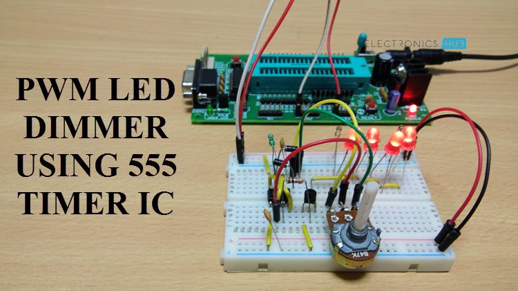
Read this post to get knowledge about circuit diagram and working of PWM LED Dimmer Using 555 Timer IC. Here, we use PWM Technique to dim the intensity of light of the LED using 555 Timer IC.
limpid nest
I figured the 555 would be involved, but I don't like linking the cathodes of LEDs
I also need something that will just run when powered and not require human setting of something like a pot. I am probably best off just using a cheap MCU and programming it
distant raven
That would be the easiest route
limpid nest
Yeah that requires you to set the PWM frequency with a pot right?
I'm looking for something that electrically does what a dwell mechanism does. Thanks for the driver above, I'll probably use it in the end and abandon the breathing mechanism
distant raven
You could have a push button to set a counter for your PWM frequency
limpid nest
It's gotta be completely human free unfortunately
So I have to get super old school or break down and program something
distant raven
Or just a timer that slowly increments a counter for setting your frequency
limpid nest
Yeah that would need programmable silicon though right? I'm seeing if I can avoid that
TBH programming something is the optimal solution, but I've gotten myself curious
distant raven
It would probably be pretty complicated to do it without a microcontroller
limpid nest
Yeah
To use a 555 for example you'd need something that varies a resistance with time, no?
distant raven
It’s doable, but probably more trouble than it might be worth outside of education
limpid nest
Yeah
distant raven
You could use a counter that you use a say, 4:2 decoder to trigger different paths for your 555 resistor
That you would use to control the timing
Then use another 555 in astable mode to clock the counter every 30 seconds or something
distant raven
Oh, easily
limpid nest
plus a QT py can change the effect
or can be changed
When you found those PMIC LED drivers, what did you use to make sure they would work without like a SPI or I2C signal?
distant raven
But if all you have is a bunch 555 , counters, and decoders, you could do a lot
limpid nest
limpid nest
When you found those PMIC LED drivers, what did you use to make sure they would ...
I'm just using PWM dimming for now
as a parameter
distant raven
I’m not sure if there are any ones that support i2c or SPI
limpid nest
Any ones that are hardware only? That's what I was gambling on, but I'm still getting ones that are serial based
distant raven
I think most if not all are able to operate without a microcontroller
You just need a pwm source of you wish to dim them
 frigid current
Hey all, looking for some help with a PCB I'm working on. I got prototypes and they're not working as expected
I'm trying to make a USB-C switcher
Here's my circuit diagram

I'm using a rotary switch (center) to have one input USB-C receptacle switch between two output receptacles. I thought I could pass the CC pins through to allow for native USB power delivery negotiation. But when I soldered up the boards, that didn't work at all
Luckily I don't really need that feature, the only thing I want about USB-C for this project is the nice plug form-factor
So I soldered on some resisters to pull each receptacle's CC pins to ground:
(this tells the USB host to treat the device like USB-B, ignoring USB-C-style power delivery negotiation and other fancy stuff, and just connecting using normal VBUS, GND, D+, and D- pins)

The circuit digram should now be:

(I know ideally these should be 5.1kΩ resistors, and ideally there should be one for each CC1 pin and one for each CC2 pin, but I think using one resistor for both CC pins usually works fine, and I think the resistance is pretty flexible)
Now when I plug in my keyboard to the input, and two computers to the outputs (Host A and Host B), only one of them will work. And what cable I'm using starts being an issue: if I plug the keyboard directly into my MacBook, any of my 3 cables works, but if I'm going through the PCB, my computer seems to need a certain cable that came with my keyboard on its side of the system, and won't make the connection if I'm using either my fully-featured 10gbps USB-C cable from my hard drive, or my MacBook charging USB-C cable. Again any of these work when connecting directly.
Any idea what's going on here? I have a few ideas
- maybe the fact that I'm sharing ground between all three receptacles isn't good, and is messing up various things
- Before I grounded the CC pins, maybe the fact that B8 and A8 weren't connected was making PD negotiation over CC not work? Although I thought that would work fine...
ember laurel
I need TEA1716T/2,518
The world has gone crazy - lead time for this chip is 76 weeks right now
supple pollen
frigid current
(I know ideally these should be 5.1kΩ resistors, and ideally there should be one...
The Raspberry Pi people made that mistake, and it caused them a fair amount of trouble.
supple pollen
ember laurel
The world has gone crazy - lead time for this chip is 76 weeks right now
Lots of people are building power supplies, and increasing regulations are requiring PFC
still sphinx
ember laurel
I need TEA1716T/2,518
https://www.ebay.com/itm/194288857705
I found this if you don’t mind paying inflated prices

eBay
TEA1716T 10. We are always willing to work things out. If we know about it, we can fix it. Italy and other countries.
frigid current
supple pollen
The Raspberry Pi people made that mistake, and it caused them a fair amount of t...
I wouldn't implement it this way for a final, but for this test I thought it would be enough. Maybe not. I'll set up a breadboard with properly grounded USB-C receptacles (https://www.adafruit.com/product/4090) and see if I still have a problem

Throw out all those Mini and Micro B USB cables you have in a plastic bin - the next generation of USB connectors is here with USB C! You will start to see these connectors pop up on all ...
Any idea about why the first setup didn't work though? I thought passing through CC would be fine
ember laurel
still sphinx
https://www.ebay.com/itm/194288857705
I found this if you don’t mind paying infl...
Says only 9x10 available
I need 525 units
worldly schooner
frigid current
Any idea about why the first setup didn't work though? I thought passing through...
If this is a passthrough, you could instead skip the resistors and pass CC1/CC2 directly? The power negotiation is usually handled by devices, not cables, anyways.
Though you definitely should keep the two separate from each other, otherwise your negotiation circuits are going to have some funky readings.
frigid current
@worldly schooner that's what I tried first, and it didn't make any connection at all
frigid current
frigid current
Here's my circuit diagram
See this circuit diagram
I thought this would basically make the devices oblivious to the fact that there's anything in between them, but something about that didn't work.
Do you think common the common ground between the two hosts and the keyboard would mess things up?
worldly schooner
It's probably the crossing of CC1 and CC2? Try keeping those signals separate?
frigid current
Ooohhhh
Aw crap well my Rotary switch doesn't have enough poles to be able to do that 😦
Actually I don't think it's a problem to cross CC1 and CC2, see this article:

This introductory article will look at some of the most important features of the USB-C standard.
Connecting the USB Type-C cable creates a current path from 5-V supply to ground. Since there’s only one CC wire inside the USB Type-C cable, only one current path is formed.
So if there's only one wire, connected the two just makes sure that that wire is passed through no matter the plug orientation
(and admittedly plug orientation detection will be disrupted)
elder peak
tl;dr: Sourcing power factor IC's not everybody's cup of TEA today.
ember laurel
Slow clap
limpid nest
How weird is it for a chip to have a punch of external passives but the datasheet lacks any guidance for picking those passives?
fervent lance
I opened an electronics for the enclosure but the PCB had mounting one and one of them had metal around it
was it some sort of debug port/test point ?
worldly schooner
Mounting hole with metal?
That's pretty standard for any kind of metallic enclosure, as the plated hole can serve as a connection to earth?
Sometimes PCB designers just default to plated holes for reducing the likelihood of screws scraping fiberglass particulate from within a PCB hole.
@fervent lance Usually test points are fairly small circular pads, it's unlikely they would use a mounting hole for a test pad.
limpid nest
EAGLE users. Is the pattern tool just awful in EAGLE too? I didn't use it a lot before I switched to Fusion. It's truly bad in Fusion.
distant raven
Yeah it’s not great but better than fusion in my experience
limpid nest
Oof
I legit don't think it's going to save me ANY time to pattern something that should absolutely be patterned, if the tool worked.
supple pollen
My approach is save the object, write code to generate the script or XML to generate the pattern with the objects, and re-import/run the modified file. I know that's not the approach for most people, but it puts things in the realm where I have absolute control, which is how I like it.
When I ultimately make the switch to KiCAD, I can just embed my ideas of reality directly in the code (and submit pull requests in the hope that someone else wants that behavior)
limpid nest
I think when I have a serious pattern to do, I'll try htat
supple pollen
I built a custom footprint the same way, and even numbered 3/4 of the pins correctly...
pure gorge
This is one of my first PCB designs so go easy on me, but any feedback or things I did wrong here? I know I probably messed something up on the CP2102N or ESP32, and I could probably squeeze the whole board into two layers if I try hard enough.

 unreal flax
pure gorge
This is one of my first PCB designs so go easy on me, but any feedback or things...
unreal flax
pure gorge
This is one of my first PCB designs so go easy on me, but any feedback or things...
I have not done a thorough review, but at first glance I'm seeing a general lack of decoupling capacitors on the various power-rail pins on each chip. Also, the C1 and C2 caps on a couple of the serial lines are unexpected, so those should probably be double-checked.
It's not obvious to me that you're going to be able to flash the ESP32, since the various boot-mode pins don't seem to be hooked up in any controllable way.
pure gorge
Ok, i was following the ESP32 datasheet for the typical usage and probably got quite a few things wrong
This was originally supposed to be with the RP2040 but i switched to a faster processor with more SRAM
unreal flax
Espressif publishes reference schematics for a lot of their development boards, so those are a good source to copy.
limpid nest
Anyone have a good sense of how much heat a single neopixel puts out at full blast? The datasheet just basically says "it depends and it's important you get it right!"
unreal flax
The canonical current consumption is 60mA, so if you power it at 5V and all the energy went into heat, that would be 0.3W. Some of it will escape as light, but it's probably not more than 50% efficient, so I'd ballpark something like 0.2W of heat at full blast.
inland jungle
the voltage drop across a diode is typically 2-3V, so even if you power it with 5V, you'll be dissipating some of that across the current limiting resistor
 marsh nest
OK, need a sanity check.
https://www.bourns.com/docs/Product-Datasheets/70adm.pdf
Looking through this connector's datasheet. And... There's nothing I see about what pins are actually connected?
so, the drawings they have are of a 4-contact connector, with 7 pins. 4 are aligned to the contacts, and the other 3 are on the other side and offset. Logic dictates that the four aligned pins are the ones that are connected, but. I've seen some illogically designed packages in the past.
steel valve
How do SMD RGB LED work exactly? Thinking of adding onto my project
Do I need to use resistors or caps on it?
What ends up being its power draw since it can be multiple colors?
marsh nest
steel valve
How do SMD RGB LED work exactly? Thinking of adding onto my project
Depends entirely on the LED.
You have ones that are common-cathode, in which you drive the anodes differently to mix your colors.
You have ones that are common-anode, in which you drive the cathodes separately.
For these, they're effectively three different LEDs - you'll need different resistors and each color will have a separate power draw.
There's also ones that have built-in controller chips, which can use a variety of communication protocols. Ones like those found in the Neopixels use a single wire for communication, but there's others out there too.
You can also get separate ICs that will control your LEDs for you over i2c, SPI, or one of a pile of other protocols. These may or may not require external resistors.
marsh nest
Nope, not i2c, it is it's own method of doing it
steel valve
So a custom library then
marsh nest
Thankfully, Neopixels are common enough that there's plenty of libraries out there for them already
steel valve
Does mouser carry single ones? I keep finding kits or strips of them
marsh nest
Mouser? No idea. Adafruit sells them, though, and you can get neopixel compatible individual things on places like Amazon too
steel valve
Are there all in one ic's that can charge a lipo, and also take the lipo and convert down to 3.3v?
distant raven
marsh nest
OK, need a sanity check.
<https://www.bourns.com/docs/Product-Datasheets/70adm....
That seems to be the case. You could make two test designs and test continuity to verify for certain
distant raven
steel valve
Are there all in one ic's that can charge a lipo, and also take the lipo and con...
I think Texas Instruments makes something that does this but it’s not likely in stock
marsh nest
distant raven
That seems to be the case. You could make two test designs and test continuity t...
Some careful multimetering of the actual part could work too, before I go and order any PCBs.
distant raven
Probably, probing might be difficult if it’s a small part
marsh nest
It's a 4mm pitch connector, so plenty large enough. Annoying, possibly, but shouldn't be too bad
distant raven
Oh gotcha
distant raven
I have a curious moment. I see that they have these magnetic 3 pin connectors but they are right angle. I feel like it would be reasonable to be able to solder the pins SMD style to do a right angle connection. it wouldn't be a high torque set up, just a connector for an LED PCB onto a base to get power/gnd and data for neopixel designs. https://www.adafruit.com/product/5360
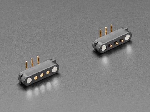
If you love power adapters or toys & gadgets that have magnetic connections, you can now experiment with these futuristic connectors easily. It's sorta like a DIY ...
supple pollen
It seems to me that would work nicely
pure gorge
Does anyone know where i can find a footprint and symbol for this? https://www.adafruit.com/product/4932

If you're a DIY enthusiast who'd like to update your project's connection to the latest USB standard, here is a 10-pack of USB C plug connectors! They can be ...
supple pollen
You could probably extract them from an AdaFruit board that uses the connector
distant raven
I think solder party boards use that
pure gorge
supple pollen
You could probably extract them from an AdaFruit board that uses the connector
Do you know of any adafruit boards that might use it?
supple pollen
Not offhand, alas
pure gorge
Ok, i found an alternative part that has a library
fervent lance
What is the part # for the the female battery connectors on the feather boards? I'm looking for that with wires attached or solder points. I want to connect them to a lipo battery recharge unit so I can easily plug in my lipo batteries and change them.
marsh nest
fervent lance
What is the part # for the the female battery connectors on the feather boards? ...
You're looking for something with wires that you're going to plug a lipo into?
It's a 2-pin JST 2.0mm pitch connector. I think they're JST-PH connectors but I'm not certain.
I do know that not all of the ones you can get match the battery colors with their wires, though
steel valve
Can I add in pads to a pcb for a circuit of parts that aren't on the pcb currently
Like an optional component area
Or would that make an open circuit
like I want to add an optional usb to ttl programmer circuit to my pcb
Since I have the space for it
unreal flax
steel valve
Can I add in pads to a pcb for a circuit of parts that aren't on the pcb current...
Yes, that should generally be harmless.
steel valve
Ok cool
Cause I am unfortunately going to have to have components be placed on the bottom of this two layerp cb
Since this time I am going to go two layer rather than four layer
So since I am going to be using bottom space I am going to cram as much useful stuff down there as possible
Like possibly adding a battery monitor ic or something down there
Since those are generally OOS but might be back one day
At least in the form factor I would want it in
Most fuel gauges on mouser have circle pads on the bottom of the ic

And I have zero idea how this is supposed to be soldered
The only thing that fits the criteria is a bit too overkill and pricey
 distant raven
Sure, BGA is just harder because you can’t see shorts under the package
But you can do it
steel valve
What about these type of smd components?

The only pads are near the edge
Which (should) mean it is simpler to solder cause it is easier to see bridges?
distant raven
Oh yeah, those are pretty easy
I do caution that anything less than 0.5mm pitch would be very unworkable without a stencil and very good solder paste application
steel valve
Oof that was just a placeholder image it does have a gnd pad in the middle oof
Ok well I guess my only option if I want to see how much is left in the lipo is to use that pricey one
supple pollen
You can also use "Coulomb counter" type fuel gauge chips, or monitor the cell voltage to get an approximate state of charge.
distant raven
Reading voltage isn’t a terrible way. I think a few Adafruit boards do that like the MagTag
steel valve
Couloumb counters on mouser seem to be even more expensive
At least in the form factor of choice
distant raven
Do a 100:1 voltage divider and tap the center
steel valve
100:1 voltage divider?
distant raven
Yeah, Adafruit does something like that on the MagTag for reading the battery voltage
steel valve
How accurate is doing a voltage divider to read it?
supple pollen
Most boards use a 2:1 voltage divider which brings the maximum 4.2V or so cell voltage into a safe range and is easily done with a pair of resistors of the same value.
steel valve
What I use is a ldo to get the thing to 3.3v
distant raven
Oh sorry, it’s 1Mohm/1Mohm
steel valve
unless you mean 2:1 voltage divider to read battery left
distant raven
 supple pollen
Yes, the supply voltage is 3.3V, so the 2:1 divider makes the maximum cell voltage (which is more than 3.3V) safe to read with an analog input.
 steel valve
So pretty much I have it like this:
USB -> USB to TTL -> MCU
USB -> MCP Charger -> LiPo
Lipo -> 3.3V LDO -> MCU
Lipo -> Voltage Divider -> MCU Analog Input
distant raven
Schematic for reference
Yeah, basically
Dang that link doesn’t seem to render for me
steel valve
epic embed fail
steel valve
What are other useful things to put on a pcb
Aside from a Charger, LDO, USB To TTL, Voltage Reader, and a button that puts the mcu to sleep and disables everything else
supple pollen
LED for testing?
steel valve
Oh yeah forgot to mention yeah that is already there
When the button is held for x amount of seconds, the MCU changes the color of a RGB LED and does stuff accordingly
Like for example holding it for one second turns it on/off (sleep), holding it for three seconds makes it go into pairing mode, and this all makes the led change color or flash
I just have not decided what rgb led to use
I would like to use one that doesn't require external resistors and the work is done via the mcu using a library, such as a Neopixel, but I can't seem to find anything that does that on mouser that is sold in singles
Since I don't need 10 I need like five
supple pollen
Resistors aren't hard. If you're making a PCB, you can even use a resistor array to reduce part count.
steel valve
Yeah I was thinking of using a resistor array
Since I do have some sections that have multiple resistors
Like for example the USB C requires two 5.1K resistors for pulldown on CC1 and CC2
Also, why does a USB C require that value specifically?
Tryna see if I can use a resistor that I use in other circuits for the USB C
Since it would save a bit to just use a resistor I am buying a lot of
supple pollen
That value was presumably arrived at by a process of dodging values that would be near what circuitry would draw, as well as values already used by various manufacturers to signal an assortment of semi de facto practices for pre-existing charging capabilities, as well as not drawing too much current.
distant raven
USB C spec says 5.1K is a standard value that will negotiate the max current of 3A, pull ups of 10k and one or two other values negotiate lower current on the up stream side (source).
ST covers it nicely
inland jungle
distant raven
Oh sorry, it’s 1Mohm/1Mohm
wouldn't you get a messed up reading unless the input impedance for the measurement was >>1MOhm?
distant raven
inland jungle
wouldn't you get a messed up reading unless the input impedance for the measurem...
Look at the schematic
The idea is the voltage divider is center tapped because it evenly splits the voltage, and the 1Mohm resistor from VBAT to tap is a very small current so it doesn’t damage the MCU pin
inland jungle
distant raven
Look at the schematic
that's not the issue. If the input impedance of the MCU pin is <1MOhm, then it's essentially acting in parallel to the bottom resistor of the divider
and changing the effective voltage division
distant raven
It works for the MagTag
Besides impedance and resistance are different even if they have the same units
They imply different things as you consider different variables like frequency of the voltage, and whatever the imaginary component of the associated CL components
inland jungle
sure, and typically analog inputs are measured by charging up sampling capacitors through the input impedance
distant raven
Which is likely why Adafruit includes a 0.1uF capacitor as it changes the impedance of the battery tap
inland jungle
yeah, that might solve the issue if the sampling caps are much smaller
supple pollen
inland jungle
wouldn't you get a messed up reading unless the input impedance for the measurem...
Correct. However the input impedance is indeed very high, so it doesn't affect the measurement much.
steel valve
What copper pour clearance is recommended for two layer 0.8mm thick boards that do RF stuff
supple pollen
For radiating components (like chip antennæ), the data sheets will have guidelines.
limpid nest
For EAGLE/Fusion, does anyone have experience doing a "pad in pad" footprint? e.g. a footprint that both a thru hole and an SMD pad? I'm trying to recreate a QT-PY footprint that I had some issues using
unreal flax
Normally I'd do that as an SMD pad plus a via.
limpid nest
unreal flax
Normally I'd do that as an SMD pad plus a via.
Via in the library editor?
That's a good idea
Thanks, I'll try that
still sphinx
I used this https://www.instructables.com/PCB-Coils-in-KiCad/ python code to make pcb coils in kicad, and i added the output to the pcb file, but nothing happened.

Instructables
PCB Coils in KiCad: A few weeks back I had made a Mechanical 7 Segment Display that uses electromagnets to push the segments. The project was so well-received, it even got published in Hackspace Magazine! I received so many comments and suggestions that I had to make a…
unreal flax
Oh, good point, I'm not sure if the library editor has a via tool. The alternative would just be to create two pads and tie them both to the same schematic pin in the device connection dialog.
limpid nest
Yeah that's what I was thinking
thanks
Hmm, I'm here:
I'm just editing a footprint I had issues with to see if I can fix the issues that way. This is what shows up when I use New in the package manager. Should I just name it like QT_PY_MOD?

Should a PWM input pin have a pullup if it's also an EN pin that enables the chip when it's high?
unreal flax
limpid nest
Should a PWM input pin have a pullup if it's also an `EN` pin that enables the c...
That sounds unusual. Wouldn't the chip be disabled whenever the PWM signal goes low?
unreal flax
Oh, I see. So the PWM is basically like flicking the light switch on and off really fast, basically turning the chip on and off. Up to you whether you want it to default to be on or off.
steel valve
supple pollen
For radiating components (like chip antennæ), the data sheets will have guidelin...
The chip antenna is outside of the pcb, which is why I ask
supple pollen
So you're asking about clearance from the externally mounted chip antenna to the PCB, or traces/components on the PCB, or what?
steel valve
supple pollen
So you're asking about clearance from the externally mounted chip antenna to the...
Ok so pretty much, I have a breakout PCB for a RF Module, the Antenna & Copper Keepout Zone is hanging off of the breakout
And am trying to decide copper clearance for the copper pour on both sides of the breakout pcb
steel valve
How many volts does a digital pin output?
Is it the same voltage that the mcu is powered with?
distant raven
Usually
 limpid nest
Most (adafruit) MCU boards take 5V, but the actual MCU uses a regulated 3.3. Easy to get mixed up
steel valve
The NRF51822 by adafruit runs from 1.8V to 3.6V
And I am supplying 3.3V
So I assume it is being regulated down to 1.8V by the module?
Pretty much I have a button on my PCB that tells the NRF51822 module to go to sleep, and set all EN pins of components on the PCB to off. I want to signify this by having a RGB LED flash or change color depending on what happens
distant raven
limpid nest
Most (adafruit) MCU boards *take* 5V, but the actual MCU uses a regulated 3.3. E...
Usually pins output the voltage level of the main supply. The board input voltage is usually the same as USB, it’s then regulated down. Some pins are 5V tolerant for inputs on but don’t generate 5V signals themselves
nRF51822 should have 3.3V logic digital IO.
Or whatever the supply voltage is in that 1.8-3.6V range
steel valve
Ok so then I'll just assume it's 3.3V since that is what I am providing it
What is forward current on a led exactly, is it it's power draw?
limpid nest
Kind of
steel valve
Or how exactly do I know how much power a led will use
distant raven
Individual LEDs draw anywhere from 10-40mA with 20mA being standard for a fully driven single color
limpid nest
This isn't a perfect formula, but you can calculate the Fwd current with I_Fwd = (VSupply - VLED)/R_Series
It's the current thru the LED
steel valve
Yeah pretty much I want a LED whether it be RGB or a normal LED in my pcb, but I am tight on power
limpid nest
You don't have to run an LED at its max to get "good enough" brightness in most cases
steel valve
I am also trying to make the component placement not ridiculous
limpid nest
Heh, that can be troublesome
steel valve
So I keep swapping between using a RGB LED and Normal LED
limpid nest
normal LED is easier for sure, you can control one with just a transistor and a pin
steel valve
If I could use a Smart RGB LED like a WS2812, I would go with that but mouser does not seem to carry RGB LEDs with Drivers in them in singles
Aside from one
And it is unclear if it only runs on 5V voltage or not
 limpid nest
 steel valve
Yeah, that's why I am going with a normal RGB LED or just a single LED
Since I can communicate everything with both
Aside from not having a low power indicator
limpid nest
Yeah it's easier to just get a FET that can be switched by 3.3V or lower
steel valve
But that would probably not be used since power constraints
steel valve
No no no like the low power indicator
limpid nest
ahhhh
steel valve
Pretty much:
It is red when the battery is low on power
It is green when awake
It flashes blue when pairing
limpid nest
I can see why you wanted an RGB LED
steel valve
I'm a little tight on space on the top layer of the pcb, which is where the rgb led would go
And I use 0603 components
steel valve
Which is why having an all in one RGB LED would be nice
Since I don't need the three resistors
limpid nest
I think adafruit sells a 3.5mmx3.5mm neopixel
steel valve
I could however use a resistor array
Which would save space and be cheap
But from my understanding they aren't the easiest to solder
distant raven
Easy with a stencil and solder paste
Or easier
Neopixel are a great option for RGB
5050 and 3535 sizes are easy to work with
Usually have max current draw around 50mA, though typically draw about 1/3 of that for a single neopixel
distant raven
Yeah, plus you can drive lower intensity on each channel and get decent colors
steel valve
I just wish they could be bought individually instead of having to get a 10 pack
distant raven
So instead of making it red (255,0,0) you can do (122,0,0) and get a lower intensity
Never hurts to have extra. I’ve personally bought two reels of 1500 each lol
distant raven
You can put a 0.1uF ceramic capacitor between VDD and GND
Large chains of neopixel typically like a resistor on the data line
steel valve
Yeah I only intend to use a single one
At least per pcb
And I intend to make two pcb
distant raven
Yeah, no passives really needed then
steel valve
I am making it so my PCB never fully turns off like most fancy ones do.
I can disable the charger, usb to ttl programmer, multiplexer, and ldo (which I wouldn't do cause that would break stuff)
From my understanding, LDO are not energy efficient and require a lot of energy
How do I figure out how much the LDO is drawing?
Or for designs that go to sleep mode rather than turning off, would it be better to use a buck.
unreal flax
steel valve
How do I figure out how much the LDO is drawing?
An LDO discards all the extra voltage between the input and output. So if you have a 7V input and a 5V output, it will be 5/7 = 71% efficient.
steel valve
Actually, what does EN do with a LDO
Or I mean
What is a practical purpose of it
And then in that case, the efficiency of the LDO is 80% min since a lipo is going to it
And the efficiency increases as the lipo loses power
unreal flax
steel valve
What is a practical purpose of it
You can use it as an on-off switch for (sections of) your circuit, for example. Disabling the LDO will also disable anything that it normally powers.
steel valve
So in the case that the LDO powers everything it should always be on
unreal flax
Yes, it's typical to just tie EN to the input voltage so the LDO comes on automatically.
steel valve
When a MCU goes into sleep mode, do sensors connected to the mcu draw power still
unreal flax
Yes, generally the sensor will not know that the MCU is asleep. Sometimes sensors have their own sleep modes which can be activated by a command.
steel valve
Yeah, the sensors are potentiometer-like (variable resistors)
So they'd just draw power too
unreal flax
If they're like pots, then they would have the resistor current flowing through them all the time, independent of whether the MCU is reading the result or not, yeah.
steel valve
Luckily the majority of them do not go through the mcu normally
10/15 go through the mux
Which can be disabled
unreal flax
I don't think that would matter either. As long as the sensors have power, they'll draw current, even if the mux isn't reading them.
steel valve
unreal flax
I don't think that would matter either. As long as the sensors have power, they'...
The stuff going through the mux require a voltage divider that is at the output of the mux to be readable
Would they still draw power while being half of the voltage divider circuit
unreal flax
Oh, good point, I had forgotten you put the divider on the output side. In that case, they would indeed not draw current when the mux is de-selected.
steel valve
Ok cool thought so
There are seven voltage divider sensors that I assume would always be drawing power then
What would be the best option for cutting them off?
And does a neopixel draw power when the led is turned off?
unreal flax
One option for the voltage dividers would be a FET on either the high or the low side, so you'd switch them on right before taking readings, then disable them again.
The Neopixel would draw some power, since it needs to be monitoring the data pin and echoing signals for the other LEDs in the string, but I'm not sure what its quiescent current draw looks like.
A quick search online suggests about 1mA minimum current draw, though it may vary with the specific type of pixel.
steel valve
Yeah that is what I found too
I might have a simpler way to do this
Pretty much on my PCB there are a crap ton of through holes on the edge
And they have unevenly distributed voltage holes
So I have on the top layer of the PCB a long strip that goes around the pcb in a loop-de-loop
And I could put the mosfet there
That would completely disable every external sensor
Yeah since my first pcb failed cause I put the wrong type of switch on it and the usb c hole was a bit too small so this time I am adding in everything I want, and making it two layer
The top layer solely controls power excluding the rf module
It contains the charger, ldo, led, button
The bottom has everything else, mux, programmer + breakout pins for an external programmer, etc
steel valve
I have two options, have a trace go straight to its destination on the top layer, but a chunk of gnd pour is gone, or make a trace go underneath the pcb and come back up with a via to get to its destination but there is significantly more ground pour.
What is the better option?
I assume it is the via?
steel valve
Also, what is more important, a signal trace being shorter or having more ground plane (in a compact two layer pcb)
supple pollen
steel valve
What is the better option?
As in most engineering decisions, it depends. If the trace is carrying a high speed signal, it may make sense to optimize it. If the ground pour being lost is under a bunch of traces carrying high speed signals, it may be worth avoiding that.
 fiery parcel
Hey all, I'm using a PN532 receiver for one of my projects but I want my antenna to be in a specific shape. What are the chances I would be able to design my own with PCB design?
worldly schooner
fiery parcel
Hey all, I'm using a PN532 receiver for one of my projects but I want my antenna...
https://www.electronicdesign.com/technologies/passives/article/21769333/electronic-design-welcome-to-antennas-101
tl;dr not impossible, but also not ideal. You could certainly make a simple one if you have enough technical understanding of basic RF concepts, but it's not a trivial task and the returns for it are limited. Unless you're really particular for ideal aesthetic over ideal function, I can't say I would ever think it's worthwhile, but it would make for an interesting experiment.
fiery parcel
Yeah. Basically, I have this toy that has a hexagonal base that has the main board, speaker, battery and NFC reader
The antennas I’ve been using previously are too big, or too small. I’ve been wondering as well if I can detach the antenna from the adafruit NFC breakout. That would work too.
worldly schooner
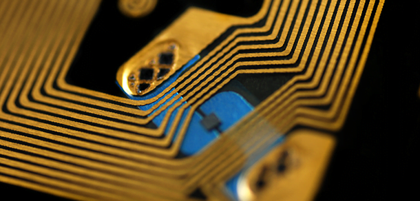
Campus card, mobile credential, identity and security insight for education markets.
fiery parcel
Thanks for sharing!
steel valve
supple pollen
As in most engineering decisions, it depends. If the trace is carrying a high s...
The NRF51822 uses a 16MHZ ARM Cortex processor so I am prioritizing ground since I can't via stitch the ground in this case due to the limited area to do so
ember laurel
does anyone have any good tips for an LDO that handles 40V input, 9V output, and a very low load?
(and also doesn't require a ton of current on the adjust pin)
I was using the SY6345, but it has disappeared from the face of the earth
I really only need to pull some 3mA
LM317 doesn't handle regulation when loaded with less than 10mA current draw.
at 10mA (through lower adjust resistors) it starts pulling quite a bit of current, due to the large drop I have.
I'd prefer to avoid a buck for this
pure gorge
Is there anything wrong with this schematic? I'm just making sure before I get it manufactured

I also don't know if the resistor values are right for the notes, I used this website to calculate them roughly: https://ohmslawcalculator.com/555-astable-calculator
ember laurel
- Your Electrolytic capacitors seem to be reversed?
10nF seems like an MLCC.
But the 10uF - is that also MLCC, and not-polarized?
pure gorge
Theyre not electrolytic, theyre ceramic. I just used a polarized library since I couldnt find it unpolarized.
pure gorge
Its a stylophone business card
steel valve
In PCB Design, how safe is it to keep a crap ton of digital signals close to each other

That traffic jam of digital signals (ignore the 90 degree turns on the bottom fixing that) pretty much can only be 0.127mm apart from each other
Otherwise this isn't gonna route
steel valve
When is something considered high speed
limpid nest
Hmmm
I've heard GHz quoted?
But I think it's a band of speeds
where it begins that is
steel valve
Yeah the NRF51822 runs on a 16MHZ processor so it's relatively low speed
limpid nest
I'm usually doing a low speed SPI or I2C bus
steel valve
But anyways yeah on the bottom layer is the signal layer, and it's just really funky looking
I'm using like everything the nrf51822 has to offer aside from a few pins and those just are not accessible in a two layer board
 edgy jungle
So I have a Pi Pico being powered via ~5V to VSYS, however, only ~1.2V comes out of VBUS. Any ideas why this is?
supple pollen
There's a diode to isolate Vbus from Vsys
 edgy jungle
So that is what's causing this voltage drop? Is there anyways to remove it?
Does it cause issues if I short VBUS to VSYS?
limpid nest
Had a wacky idea. Mounting a QT PY in the middle of a board but on pins so that the USB port is accessible. This is so that the USB port isn't too close to an enclosure wall to be used.
Wacky or reasonable?
limpid nest
let me see
distant raven
So you could probably use pogo pins to break usb to discrete headers
supple pollen
edgy jungle
Does it cause issues if I short VBUS to VSYS?
It could cause voltage to backfeed into the USB port if it's plugged into USB while powered via VSYS
limpid nest
distant raven
Or.. I think the qt py usb data pins are exposed on the bottom
I'm looking at an ESP 32-S2 bottom atm and don't see that
distant raven
Ah it might be just the m0 one
steel valve
Does I2C work on any digital pin?
I am adding an optional I2C pad since the routing of my pcb is complete
So I am using the last bit of spare space to do something useful
And the NRF51822 doesn't have any specifications on requiring a specific pin to do so, so I assume it is programmable
distant raven
Yeah, you set those in the firmware
 limpid nest
That doesn't seem to be a decoupling cap
steel valve
Why does the analog vcc need its own cap?
limpid nest
I would think to smooth any input voltage ripple
steel valve
Ok so it's kinda like a filter then
limpid nest
llike a band pass filter? ish?
steel valve
kinda
I think it is so it can filter out RF SIgnals
Since this is a RF module
And AVDD is very close in proximity to the antenna
But anyways, now I have everything done aside from the voltage going to the components
I have a LiPo battery that has to go to two things, a capacitor from the charging IC, and a voltage divider circuit so the voltage can be read
The LiPo + has to go through the resistor of the voltage divider to get to the capacitor
Would issues occur from this
distant raven
Looks like AVDD is for generating an analog reference voltage
steel valve
But that's what AREF does
steel valve
 steel valve
(Datasheet BTW)
https://cdn-shop.adafruit.com/product-files/4076/4076_specificat...
steel valve
steel valve
(Datasheet BTW)
https://cdn-shop.adafruit.com/product-files/4076/4076_specificat...
Yeah this is the sheet
But there are multiple AREF
And this is the NRF51822 datasheet since the adafruit sheet sucks

 steel valve
So I assume that means the module board itself has no cap and wants an external one?
distant raven
My guess is Adafruit probably expected more noise on AVDD or didn’t include one on the module.
steel valve
 supple pollen
steel valve
The LiPo + has to go through the resistor of the voltage divider to get to the c...
supple pollen
steel valve
The LiPo + has to go through the resistor of the voltage divider to get to the c...
It shouldn't go "through" (series) at all, the voltage divider is normally in parallel.
steel valve
This is my only ref image of the internals
steel valve
supple pollen
It shouldn't go "through" (series) at all, the voltage divider is normally in pa...
wdym
supple pollen
There should not be a series resistor to the LiPo
steel valve

The arrow is the direction the lipo is entering
The three diode line is the voltage divider for reading the voltage of the lipo
And the two to the right are the caps that go from the charging ic to the ldo
supple pollen
That picture is singularly uninformative, and I don't see any diodes at all. Do you have a schematic?
steel valve
 supple pollen
Like I said, there is no series resistor, the connection goes from the LiPo to the regulator.
Oh, do you mean the capacitor across half the voltage divider?
steel valve
yeah
supple pollen
That just forms a combination voltage divider (to sample the voltage) and an RC filter (to smooth out variations in the voltage). It should be totally fine.
steel valve
The LiPo connects like this

It goes through the bottom pad of the first resistor of the voltage divider in order to connect to the capacitor of the charger
supple pollen
The charging current, however, does not go through the resistor, it just goes through the pad.
steel valve
Ok cool
Then another routing question is, can the capacitor for the charging circuit connect to pin 1 of the ldo, that is connected to its respective cap
 supple pollen
Yes, those capacitors are effectively connected together anyway. Often the capacitors will be physically close to the various units, so they can give the best effect.
steel valve
Ok so it doesn't matter which order it is connected (doesn't have to be linear)
supple pollen
Generally not. Since you have RF signals nearby, things can't be too far, but it doesn't need to be linear.
steel valve
Yeah everything is as close as it can be while being easy to assemble
supple pollen
That's a good thing to keep in mind!
steel valve
Now I just need to ground stitch, and then add in a mosfet that the mcu controls for the sensors
Since ten of the variable resistors go through a multiplexer, which can be disabled when in sleep
But five of them do not go through the multiplexer
And they draw ~1.3 milliamps
Which would drain the battery in only 100 hours or so assuming it was at max charge
supple pollen
So you'll use the MOSFET to switch the power to the variable resistors?
steel valve
supple pollen
So you'll use the MOSFET to switch the power to the variable resistors?
Yeah
When the MOSFET is enabled, it allows the voltage to travel to a long trace where the variable resistors are
 untold moat
@supple pollen You have used the Sparkfun Artemis Module in the past from what I read, what issues occurred with it that made you not like it?
supple pollen
The board package was incompatible with the board. I tried installing a dozen or so different previous versions, but none of them would talk to the board.
untold moat
supple pollen
The board package was incompatible with the board. I tried installing a dozen o...
wdym by board package being incompatible with the board
supple pollen
I mean I was unable to load software onto to board to run (even the basic blink sketch)
supple pollen
Presumably the bootloader changed over time, and there's no support for the early version (which I have)
untold moat
Why not ignore the bootloader and program via SWD
(or jtag)
Is the bootloader a requirement?
supple pollen
I'd have to find a way to hook up SWD (no connector is populated), find something to produce the signals, find the right software, etc. There's a limit to the amount of trouble I'll go to when I have plenty of other projects to do, and the board doesn't bring any particular functionality I need. I'm spending more effort on trying to get my gimbal driver board working, as it has abilities I can use.
untold moat
Isn't D21 and D20 SWD Pins?
But yeah good point it is annoying to have the external software
supple pollen
A bootloader makes the board so much easier to use (SparkFun promised "blinking in 5 minutes": after several hours with no success, I threw in the towel)
untold moat
So it is just because yours is an original version
supple pollen
Presumably.
untold moat
By the way how did you get it on your board?
Like soldering it
Isn't it annoying to place it down
supple pollen
I didn't, I just bought the SparkFun Artemis Nano
untold moat
Ah
I have been trying to find people actually succeeding in putting it onto a board since there are a bunch of pads and if one gets messed up it could cause issues
The only thing I have seen is someone placing solder only on the pads they intend to use
Which would solve the problem
supple pollen
I suspect you'd need good soldermask, stencils, and hotplate/reflow to reliably solder the little carrier board
I had planned to use the entire Nano as a daughterboard (the same way I use Teensy, Trinket, and ItsyBitsy boards)
untold moat
I intend to use the module itself since it seems to be the best RF module available on paper
supple pollen
So the Artemis joins the nRF chips in the "parts I no longer care to use" category
untold moat
What do you use instead for RF?
supple pollen
I've gone with the TI and Cypress chips
supple pollen
Heh, agreed
untold moat
Segger is annoying to use, and nRF modules are constantly OOS
(Also not as power efficient as others)
Apollo3 modules are typically hard to put onto a pcb
Have another crap sdk
But are a good bang for your buck considering how powerful and low power they are
^ Also are in stock consistentlyt
supple pollen
The TI CC2650 is pretty power efficient. The RF430 chips are ridiculously power efficient, but they're NFC, not RF
untold moat
Any sort of Arduino support for the TI CC2650?
supple pollen
Hmm, I actually don't remember. I used the "Energia" port of Arduino to the TI MSP430 chips, which was pretty painless.
untold moat
Has an all-in-one module been made for that chip
supple pollen
Yeah, they call it "SensorTag"
The last ones I used were the CC3100 modules, which are less power efficient, but fairly easy to integrate with a separate CPU
supple pollen
The CC3100 has a goofy footprint
 untold moat
Wow that really is goofy
supple pollen
Worked, though
 untold moat
I am not experienced with pad only pcbs such as the artemis-- should I apply solder paste to only the pads I intend to use, or should I put it on everything
supple pollen
I'm not sure what the best practice is there. I'd kind of lean toward putting paste on all the pads (for better mechanical stability and levelling) but I'm no expert on such things
untold moat
Yeah, I have not been able to find anything on google for these tricky types of components
The closest I have been finding is bga component soldering
Since that (should) be similar in how it works
Pretty much anything with those solder balls on the bottom
The only other idea I have to make it simple to place would be is to make an aligner of some sorts
Like a 3D printed jig that matches the outline precisely
Then there would be a very low chance of failure
supple pollen
A bunch of guidance here (specifically for QFN and SON packages, but referenced for other modules): https://www.ti.com/lit/an/slua271b/slua271b.pdf?ts=1652254845469
They get very detailed in the recommendations for some modules, one specifies "pads 56-63, 79% solder coverage, pad 55, 77.5% solder coverage". Wow.
That's for a 0.125mm thick stencil, specifically
Stuff like this actually happens, happily
 untold moat
Ok so it is more forgiving than I thought
I was thinking if it is slightly out of line the whole thing would fail
limpid nest
supple pollen
Stuff like this actually happens, happily
Also a good representation of me putting my socks on
supple pollen
It's cool to see it happening: https://www.youtube.com/watch?v=_5lksMvmqQc

We taught a SMT soldering class at the Atlanta hackerspace ( http://freesideatlanta.org ) focusing on using stencils and solder paste. Here are some shots of a circuit being reflowed on a skillet and inside a toaster oven. Surface tension is able to pull the chips into alignment.
Recommended Products:
chipquik removal kit, lead free: http://amzn...
untold moat
When is an external analog to digital converter a better option than using an analog multiplexer
unreal flax
untold moat
When is an external analog to digital converter a better option than using an an...
One reason would be that you need higher resolution than the internal ADC can provide. Or if you need to simultaneously sample multiple channels instead of doing them sequentially. Or if you need to sample a differential signal.
untold moat
At what speed is that beneficial, I intend to use a 96MHZ MCU in my project.
unreal flax
Speed is kind of orthogonal to those considerations.
You might be speed-limited by the internal ADC, or by the communications bus (SPI, usually) to get the readings from the external one.
untold moat
I intend on reading from multiple analog sensors, but unfortunately, the mcu does not have enough analog channels
Which is why I would need to use either an External ADC or Multiplexer to do so
How much faster would reading channels all at once be compared to reading them sequentially
unreal flax
It wouldn't really be any faster, since you'd still have to read out all of the data the same way. It's just that some applications care about exactly when the reading is taken, instead of having data that's misaligned in time.
untold moat
Ok, so a multiplexer would be better for my usecase then.
unreal flax
Yeah, if the performance of the internal ADC is otherwise fine for your needs, a multiplexer would do the job.
steel valve
Speaking of which
What happens when a potentiometer goes through another half of a voltage divider
Essentially, I want to put both my half voltage-dividers and full voltage-dividers in the same multiplexer
At the output of the mutiplexer is one resistor
Which does the voltage dividing for the half voltage divider sensors
unreal flax
That would cause a nonlinear distortion in the potentiometer mapping, since you essentially have a three-legged divider between the two halves of the pot and the extra resistor. It's something that you could potentially correct for in software, I think, but it's not something that would be typically done.
steel valve
So, bad idea basically
unreal flax
Easier to avoid if you have the option, yeah. It would probably be slightly simpler if you left one side of the pot disconnected and just used it as a rheostat instead.
steel valve
Would it still function the same
unreal flax
No, it would be different because of the extra resistor, just easier to correct for in your code.
steel valve
No as in using the potentiometer as a rheostat (two pin)
And then connecting it to the mux
Or did you mean that
unreal flax
Yes, that's what I meant. The readings would be different than a normal potentiometer, just less complicated than the three-sided divider scenario.
steel valve
Ah
I am trying to make cutting off the sensors in the pcb simpler than doing a loop-de-loop
And then having a mosfet
unreal flax
The rheostat mode would do that, at least, since no current would flow through the pot when the mux had it de-selected.
steel valve
In order to interface this with a microcontroller, supposedly I need to use a pull-up resistor on STAT (so that I know it is charging, when it is done, bla bla)
How do I figure out what value?
unreal flax
Are you using it with a LED or just as a GPIO input?
unreal flax
The easiest would just be to use the GPIO's own internal pullup setting, then. But if you want an external pullup, 10k is typical, or higher if you're especially power-sensitive.
steel valve
Do most gpio have internal pullups?
unreal flax
Most, yeah. It's not guaranteed, but it's a good bet if you're using a mainstream MCU.
steel valve
If a mcu has an internal pullup
Is there any benefit to having an external one
Just power efficiency?
unreal flax
The internal pullup is generally too weak for things like I2C buses, so you'd want an external one in that case, for example.
steel valve
Do I need to use 3.3V from an external USB to TTL if my project is always running
supple pollen
steel valve
Just power efficiency?
Generally not even that, the internal pull-ups source about 75µA for many common chips
supple pollen
steel valve
Do I need to use 3.3V from an external USB to TTL if my project is always runnin...
I'm not sure what you're asking. The old TTL logic family runs on 5V.
steel valve
supple pollen
I'm not sure what you're asking. The old TTL logic family runs on 5V.
Most modern external USB to TTL have an external 3.3V/5V Jumper
Do I need to use them if my pcb is already powered
 hidden night
I think that’s for setting the logic level voltage so you’d probably want to match it up with whatever your board uses. That’s how it works on the one I picked up
steel valve
Well the thing has a jumper to set the logic level voltage
Which wouldn't that mean if my board is already running at 3.3V and is powered I wouldn't need the USB to TTL 3.3V external jumper
limpid nest
re: thermals. My inclination is the 4 X (Smaller thermal size) is better than 2 X (Larger thermal size) if the width of the smaller thermals is such that 4 x (One Width) is greater than 2 x (One Width) for the larger size. Does that make sense and is that true?
steel valve
If a MCP73831 has no LiPo battery connected and is being powered, what happens?
Does it just make a 4.2V output anyway?
Also, what happens if a LiPo battery is connected to a MCP73831 and the MCP73831 is being powered, and the LiPo is connected to the rest of the pcb?
supple pollen
steel valve
Which wouldn't that mean if my board is already running at 3.3V and is powered I...
Some of those adapters have two jumpers, one for logic level and one for supply voltage. Since your board is already powered, you don't need the supply voltage, so you'd just set the logic level correctly.
supple pollen
steel valve
Also, what happens if a LiPo battery is connected to a MCP73831 and the MCP73831...
The ones I've seen supply some voltage, then see the voltage go up, so they shut off thinking the (nonexistent) cell is fully charged, but then the voltage goes down, so they switch the voltage back on, and just oscillate like that.
steel valve
So would I need to modify anything to make it so that the PCB can be charged while running
The PCB never turns off, it just goes to sleep
Pretty much.
USB C (5V) -> MCP73831 (4.2V) -> LDO <- LiPo (4.2V-3.2V)
Would it be a better idea to put in a switch instead
So that when USB C is applied, it uses the 5V of that to power the rest of the pcb
Rather than the LiPo
So it isn't being charged while being used
supple pollen
I really don't know how to keep a cell charged while it's powering something. I might use steering logic to power from USB when it's available and charge the cell, and run from the cell when USB voltage isn't available.
steel valve

What does this symbol mean
(D4 and D3)
Are they schottky diodes?
This is apparently a voltage select circuit
inland jungle
yeah, schottky diodes
used because they have a lower voltage drop typically than normal diodes
steel valve
How does this circuit work exactly
inland jungle
VIN gets powered by V_USB or V_BATT, but you can't backfeed the voltage from V_USB to V_BATT or vice versa...keeps your battery from frying your USB port, for example
steel valve
Wouldn't that make both USB and LiPo able to power the circuit simultaneously
I assume a mosfet is the better option then if I only want one powering everything at a time
distant raven
It is
Schottky diodes are great and all, they collapse and recover very quickly which is great for ESD protection on usb lines, but it’s suboptimal for voltage selection. A p-chan mosfet is much better
Adafruit does this on all their current feathers
And more importantly what we’re seeking to block is sending current the wrong way on the USB line since when USB is connected we are very likely charging a LiPo, the mosfet acts like a diode in those cases. It’s just better overall
steel valve
What's the schottky diode for in the adafruit circuit

Since it has a mosfet, wouldn't that make the schottky useless
distant raven
Still ESD protection
Plus current protection as well. Limits the overall draw of the feather
steel valve
Ok so its best to add both in a pcb like that
distant raven
Yes
steel valve
USB C PD can request a specific voltage & amperage, from my understanding this is configured by the CC1 and CC2 pins
distant raven
Yes
steel valve
How do I figure out what resistor to use?
steel valve
Is USB C minimally 5V? Or can usb pd set it to be lower
supple pollen
steel valve
Since it has a mosfet, wouldn't that make the schottky useless
Nope, the Schottky protects from Vbat going to Vbus, the MOSFET provides a low-loss connection when Vbus is unpowered.
steel valve
So it's preventing reverse voltage

Why is a resistor used on EN?
Does it not work with V going there normally
limpid nest
supple pollen
Nope, the Schottky protects from Vbat going to Vbus, the MOSFET provides a low-l...
What's the pt of the 100k to ground?
steel valve
Yeah that too
Also, for a p-channel mosfet and shottky diode like the ones they use, what parameters do I need to use to get one that would work for its purpose?
supple pollen
limpid nest
What's the pt of the 100k to ground?
That pulls the MOSFET gate down when there's nothing connected to Vbus.
supple pollen
steel valve
Why is a resistor used on EN?
That sets a default of "enabled", but lets an external signal override it if someone wants to.
supple pollen
Yeah, you can just tie the enable pin high.
steel valve
And R12 is always required
supple pollen
Yes, otherwise the MOSFET will just have its gate float randomly when nothing is connected to Vbus
limpid nest
yes
steel valve
Also why is it 100K?
supple pollen
It's high enough to not waste too much power when Vbus is powered, and low enough to keep random noise from affecting the gate voltage.
steel valve
Ok that makes sense
Then, do the mosfet and shottky have specific parameter requirements?
supple pollen
Generally, yes.
steel valve
On mouser there's a crap ton of parameters that can be selected for them
supple pollen
The easy way out is to look up the parameters of the ones in the AdaFruit design and look for similar units.
That is assuming that your use case is roughly equivalent.
steel valve
What exactly do the parameters mean

And yeah both are wireless boards
That are bluetooth low energy
supple pollen
There's a decent writeup of how to interpret those specifications here: https://www.embeddedrelated.com/showarticle/809.php
One of my pet peeves is when my fellow engineers misinterpret component datasheets. This happened a few times recently in separate instances, all involving power MOSFETs. So it’s time for me to get on my soapbox. Listen up!
I was going to post...
For your use case, you can safely ignore some of them like minimum operating temperature and Gate Charge. The "Vgs th - Gate-Source Threshold Voltage" is problematic: it tells the gate voltage at which the transistor just begins to turn on. For switching purposes, this is not a particularly useful figure, you need the gate voltage at which the transistor is solidly on. But in general, lower threshold transistors will tend to be solidly conducting at lower gate voltages, so it's one way to sort through stuff before going into datasheets and looking at the conductance graphs.
limpid nest
Digikey often offers the "just turns on" and "fully turned on" voltages
limpid nest
Having a weird Fusion/EAGLE issue. I mirrored a part on my PCB but on my 3D PCB, all the silkscreen still appears on the non-mirrored side of the board.
Anyone have guidance?
Nevermind, it just decided to sort itself out
Weird!
steel valve
supple pollen
There's a decent writeup of how to interpret those specifications here: https:/...
what about schottky diodes how do i pick the right values for those
steel valve
What trace width should I use for USB C VBUS?
limpid nest
how much current are you expecting?
steel valve
a very low amount of current
supple pollen
You'll need a reverse voltage of at least 5V and enough current to power your circuitry
steel valve
I am a bit confused on how USB C negotiations work, does setting it for 5V 3A for example make it so the USB knows that it can provide up to that amount?
unreal flax
steel valve
I am a bit confused on how USB C negotiations work, does setting it for 5V 3A fo...
You may need to clarify the question a bit. What is "it" in this context, and how is "it" setting things?
distant raven
USB PD is pretty complex and usually requires some knowledge of what kind of upstream USB PD supplies your connecting too. Usually because the max negotiable current is determined by the upstream CC pull ups, downstream pull downs for usb c cables
I shared a ST doc the other day that explains it pretty well
Plus some software controls too
steel valve
How does routing capacitors work exactly, is it linear, where the trace has to go through the capacitor before reaching its destination, or does the trace just have to cross the capacitor when it is near its destination
steel valve
Through the pad of the decoupling capacitor*
limpid nest
It has to touch the pad
steel valve
Does it have to touch the pad before it gets to the pin
Or I mean
Directly before the pin
limpid nest
The trace?
steel valve
Yeah
limpid nest
Yeah it has to touch the pad, or else it won't be connected