
#help-with-hw-design
1 messages · Page 63 of 1
 fervent lance
ahh wait, but a voltage supervisor IC could make sure the device doesn't try to turn on if the voltage at the booster entry is too low, right?
 distant raven
Correct
fervent lance
soo question is, what specs are important here?
 distant raven
Usually threshold voltage and rise time
I think 30usec is common but you can find slower ones if the regulator has a slower rise time
fervent lance
not sure if this simulation is accurate enough, but... are -42uA on the battery + perfectly fine? If I would add another schottky diode here, the voltage from the battery would drop noticable


oh... wait... once I set 3v as the battery voltage, this would increase to -201mA... that definitely is a problem... I don't get it... am I using the wrong mosfet here?
 supple pollen
It looks like the MOSFET body diode is conducting, you may want to turn it around
distant raven
supple pollen
It looks like the MOSFET body diode is conducting, you may want to turn it aroun...
Ah yeah orientation and morning brain not serving me well here lol
fervent lance
supple pollen
It looks like the MOSFET body diode is conducting, you may want to turn it aroun...
switching source and drain? I thought source should always be where the electricity is supposed to come from and drain where it is supposed to go to
 unreal flax
That would make way too much sense...
fervent lance
in other words, that's not the case?^^
ok... now it's only nA in the simulator... that sounds better ^^
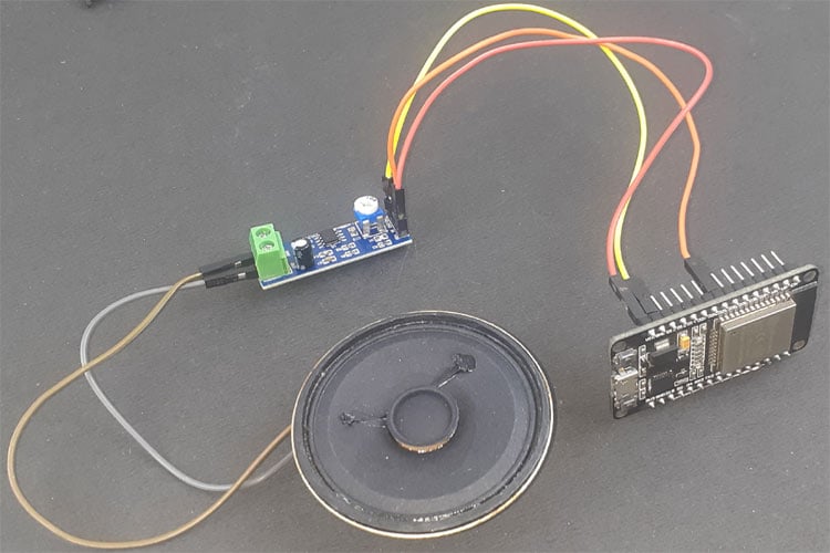
I also want to add a speaker to my LED project, for playing simple sound effects together with LED animations, based on readings of the 3 axis gyroscope I added. But I wonder if this can cause performance / memory issues with WLED (the software I use for running the LED animations) on the ESP32.
https://circuitdigest.com/microcontroller-projects/esp32-based-audio-player
 limpid nest
Would I be breaking any hard and fast rules by doing this? I want to move the !N_OE pins around so they are all next to each other, and the NA pins so they are all next to each other, and the NY pins so that they are more spaced out (!N_OE and NA pins will also be spaced out). This will make my layout prettier and easier.
 unreal flax
limpid nest
Would I be breaking any hard and fast rules by doing this? I want to move the `!...
unreal flax
limpid nest
Would I be breaking any hard and fast rules by doing this? I want to move the `!...
That should be fine. Schematic symbols have only vague guidelines about pin placements.
limpid nest
That's what I thought, thanks.
fervent lance
I can also use a regular resistor instead of a variable one here, right? As long as I don't mind the volume being fixed?
And how could I make the volume controllable via software? are there resistors which can be controlled via a microcontroller?
 limpid nest
fervent lance
I can also use a regular resistor instead of a variable one here, right? As long...
limpid nest
fervent lance
I can also use a regular resistor instead of a variable one here, right? As long...
Yeah fixed should be fine. And yes there are! Adafruit sells 2, one is linear and one is logarithmic.
They are called digipots adafruit's are I2C.
fervent lance
https://datasheet.lcsc.com/lcsc/1912111437_Maxim-Integrated-MAX5407EKA-T_C185834.pdf
That one would also do it?
limpid nest
Do you just need 10k adjustable? It might be easiest to pick the exact chip that adafruit uses, so you don't have to write your own library. If you don't mind writing your own library, then that one might serve? looks like you have only have up to +6 volts on it (I'm not sure what the specs of the adafruit chip are off hand)
When picking a FET to switch 12V, I should pick a VDSS greater than 12 right? like at least 16V?
Actually I'm doing reverse voltage protection but I think similar principles apply
fervent lance
limpid nest
Do you just need 10k adjustable? It might be easiest to pick the exact chip that...
I am still considering if I even need it to be adjustable... maybe a fixed volume is easier/cheaper to implement for now.
think I will just experiment with placing a regular resistor for controlling the loudness and then see how it goes
limpid nest
I think that ease of adjustment order is going to be mechanical pot > digipot >> fixed resistor
good luck!
But digipot probably gives you better accuracy
limpid nest
I'm trying to pick a resettable fuse. I think I want my max current to be 2.5A. I see there are two parameters: holding current and trip current, with a deadband between holding and trip current. Should I pick a fuse with a holding current equal to 2.5A and a trip current such that the deadband is as small as possible?
Additionally, Time to Trip, does a 10s TtT really mean that this fuse will conduct X Amps of current for 10 whole seconds before tripping?
supple pollen
That depends on what your parameters are. Do you want to allow a brief overload, or a small overload for a little while, but cut off quickly on a large overload, do you want to respond to surges, or allow them, do you need to allow for temperature independence?
limpid nest
Hmm yeah, it's complicated
I am confident that the raspi people did something that works for my needs, so I've been trying to copy them, but that data isn't really available.
 spice turtle
It sounds to me like Efuses are much like regular fuses or Circuit Breakers that have a B,C, or D curve. They will let so much current through for x amount of time, usually the end electronics can handle so much, but I would say pick the shortest time needed
But TBH resettable fuses arent my area of expertise, I would search TI to see what kind of documents they have
fervent lance
I am going nuts... cannot figure out how to adapt my PCB design to flash the ESP without pressing any reset button... any suggestions? I remember the ESP32 D1 Mini board can do it. But cannot find any official schematic...
unreal flax
Typically it uses some extra serial-port control signals (CTS / DTR or whatever) with some transistors to programmatically toggle the boot and reset pins. All of the Espressif reference schematics will show how to do that in the canonical way.
fervent lance
I already implemented this part and yet it still doesn't work :/ I have searched for schematics of the esp32 d1 Mini, since I remember that esp32 board can be flashed without pressing any buttons. But all the schematics I can find look a bit different. Some have the RST pin of the CP2102 connected to nothing, others connected to a resistor, capacitor and voltage/gnd. Some have resistors at DTR, RTS, TXD and RXD of the cp2102, others don't...
 supple pollen
How do you initiate the reset on this mini board?
fervent lance
the cp2102 should do that, based on my understanding
supple pollen
Then it's probably RTS or DTR based like your diagram.
fervent lance
but what parts are important for that then?
I don't really get why I cannot get it to work
supple pollen
When you say you cannot get it to work: what have you done? What was the expected result? What was the actual result?
That's a funky little circuit. If RTS is low and DTR is high, Q3 will turn on and pull RESET low. If DTR is low and RTS is high, Q2 will turn on and pull IO0 low.
fervent lance
one mistake I did was I had the pins for the auto reset wrongly connected. So I fixed that with some wires. It might not look pretty, but should be connected correctly now. But once I connect the board to my Mac and visit install.wled.me for installing WLED and select the board, it cannot upload the software but asks me to press the boot button and try it again (and yes, then the upload works fine).


I found another schematic with this nice part that replaces the four previous components. Also check the result table next to it.
 supple pollen
That truth table doesn't match the diagram, but I suspect the diagram isn't quite correct
fervent lance
what do you mean? the formatting? or whats inside doesn't make much sense?
supple pollen
You have posted 3 different diagrams. The first one (collector to RESET) seems sensible, if a little odd. The second one (emitter to RESET) may not work. The third one (with the 6-pin chip) shows DTR connected to both bases and RTS connected to both emitters, so both transistors would turn on for DTR high and RTS low, which may not be what you want, and doesn't match the truth table in the same diagram.
The truth table does seem to match the first (collector to RESET) diagram you posted, and by rearranging the signals slightly, you could make the chip do that, but the connections in the chip diagram don't match that behavior.
If you were to switch pins 4 and 5 (in other words, connect pin 4 to DTR and pin 5 to RTS), I think the chip would implement that truth table and the behavior of the first (collector to RESET) diagram you posted.
fervent lance
oh yeah you are right, RTS and DTR have been switched, my mistake (when trying to recreate an existing schematic)
 supple pollen
Granted, an IMH3A is a bigger, easier to solder package, but it has a slightly different pinout
fervent lance
but besides that part of the schematic, what else matters to implement autoreset?
here for example they used a bunch of resistors on the USB to serial chip (U2)
https://i.imgur.com/EpE4dGj.jpg
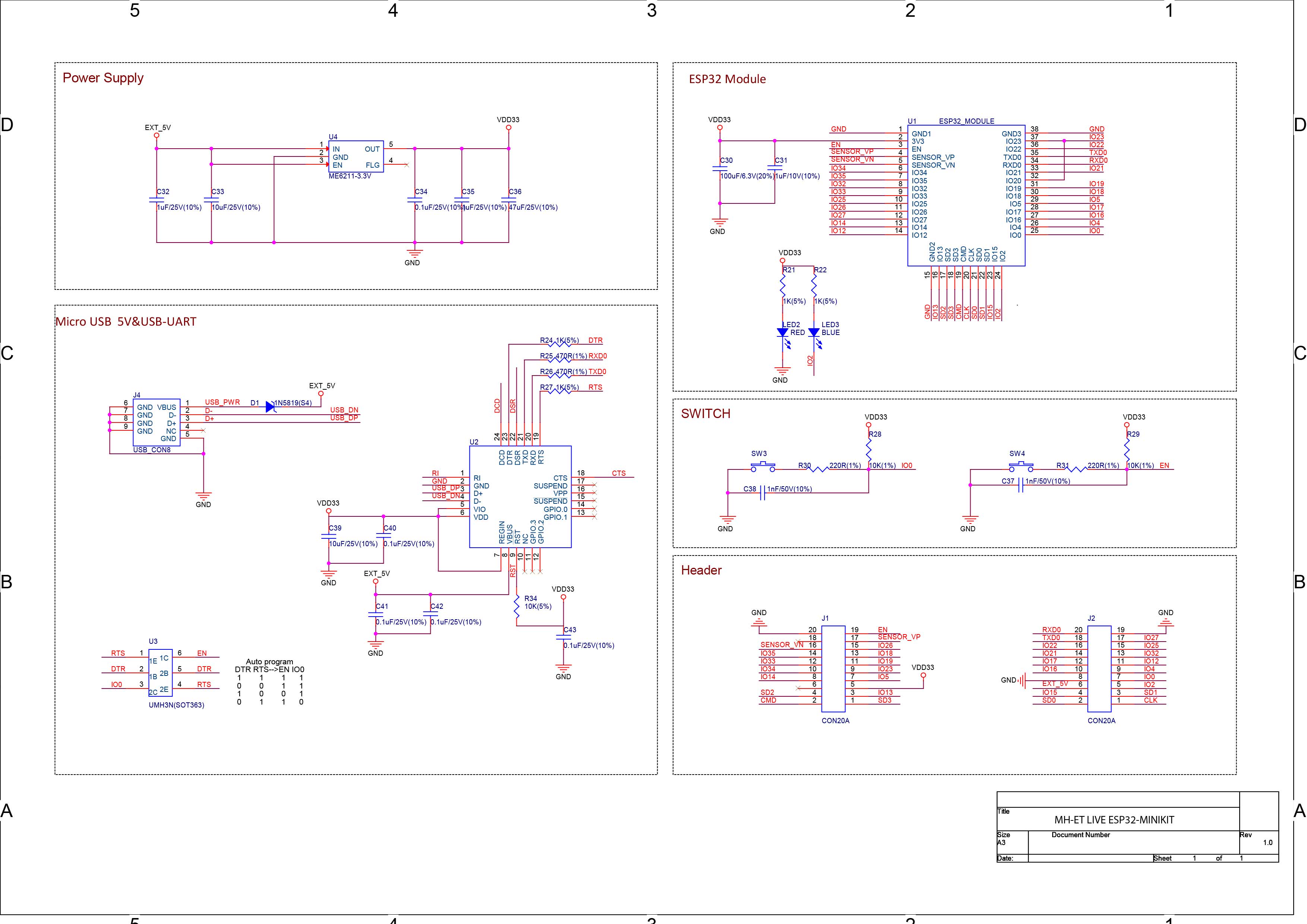
and also connected RST of the USB to serial chip. But on other schematics of the ESP32 d1 mini I found they don't do that
and I cannot find an official one for this board https://www.az-delivery.de/en/products/esp32-d1-mini (which I used in the past and know it works there)

AZ-Delivery
Dieses AZ-Delivery Entwicklungsboard mit leistungsstarkem ESP-WROOM-32 Modul, integrierter WiFi und Bluetooth Funktionalität (BR/EDR/BLE). ESP32 Chip mit TSMC-Technologie für extrem niedrigem Stromverbrauch konzipiert. Das D1 Mini überzeugt vor allem durch Robustheit, Vielseitigkeit und Zuverlässigkeit.
I already started considering if it makes sense to search for some of those boards at home (should still have them somewhere), inspect them with my macro camera and try to reverse engineer that part of the board
distant raven
Ah that’s an 8266 which is different than the ESP32
fervent lance
no, they are both esp32
distant raven
ah wait, read 8266 compatibility
fervent lance
where does it say that?
distant raven
"COMPATIBLE
It has a similar pin layout to the conventional D1 Mini ESP8266-12F and is therefore pin-compatible with most accessories for it."
at least based on the datasheet, the boot/reset strapping pins need to be toggled to achieve programability
so I think you can go with the plan you mentioned above

toggling the pins with the USB Serial
fervent lance
and the reason why it didn't work out when it tested fixing my pcb with some wires?... maybe bad soldering connections?
guess you are right... I should just adapt my pcb design, order it and the parts again and then see if it works... fixing pcbs by using wires and so on is really annoying
supple pollen
fervent lance
guess you are right... I should just adapt my pcb design, order it and the parts...
Annoying, but a big time and money saver in many cases. I'll normally hack up my boards to fix as many things as I can and ideally get them working properly, so I know I understand all the fixes required before I respin it. https://www.sparkfun.com/tutorials/109 Pull quote: "Don't immediately throw up your hands and layout a new board. Instead, make sure you get every bit of the functionality of your board working, by any means necessary, and then make all the revisions. Otherwise, you'll constantly spin your wheels with PCB revisions."
fervent lance
supple pollen
Annoying, but a big time and money saver in many cases. I'll normally hack up m...
yeah that was also my approach so far
don't worry
supple pollen
"anyone can layout a PCB, but it takes a true magician to get a bad PCB working. Scratch, cut, splice, and otherwise modify your PCB until you get it working."
fervent lance
:D:D
supple pollen
We've all been there
 fervent lance
^^
 heavy jasper
That said - there is a point that my colleagues and I call “critical jank” where any change/rework you make has a 50/50 chance of helping vs. making something worse just because of the fact that you’re doing somewhat hacky reworks. That’s where it’s helpful to order more than one board on your first order, so you can rework your way to critical jank on your first board, then take just the reworks you know you need and apply them as cleanly as you can to your second board, then start bringup again from there.
The strongest version of this being to just release a second rev of PCB with your known changes and start again from there.
supple pollen
Been there too...
 distant raven
hehe...
fervent lance
yeah can relate... ^^
oh and another important question, since my LED / PCB project is battery powered - how do I read the battery charging status? can I connect the TP4056 to a GPIO pin for that? or can i just connect +BATT to any GPIO pin from my ESP32?
 supple pollen
You'd need some signal conditioning as your battery voltage may be high enough to damage a GPIO (especially during charging). You could connect the "charge" output of the charge control chip to a GPIO, but it's open-drain, so you'll need a pull-up (either the GPIO built-in one, if it offers one, or an external resistor).
To actually monitor the state of charge would require a little more.
limpid nest
Me to Autodesk: This feature doesn't work
Autodesk: Have you tried using the feature, it's really how it's supposed to work.
Me:....
supple pollen
I had a couple of rounds of that with sheet metal fabrication in Fusion 360. However, watching a video by another company and doing some experimentation finally yielded the results I was looking for.
limpid nest
If anyone was considering switching from pure EAGLE to Fusion360, wait a while. They completely broke the library management workflow.
supple pollen
Nope, I'll use my expensive EAGLE license for as long as I can, then I plan to switch to KiCAD
limpid nest
I'm considering a switch to KiCad when life slows down and I have the time.
distant raven
I’ve contemplated KiCAD as well
I love eagle and fusion, I’m coasting on an edu license since I’m not selling anything and it hasn’t kicked me out yet lol
limpid nest
Yeah I needed a commercial CAD program that did EDA and 3D well. Fusion is supposed to be that, but they keep adding ingredients to the meal and making it harder and harder to stomach.
The 3D CAD is "fine", but they have borked the EDA pretty well.
For example....a part I just added isn't showing up on my dang board.
limpid nest
Oh of course! It created a copy of my board, dissociated it from my schematic, kept the name the same, and didn't tell me!
supple pollen
I use Eagle (and DesignWorks Lite) for PCB design, and Fusion 360 (and OpenSCAD, and pencil and paper) for 3D design.
limpid nest
I prefer Inventor but I can't afford it
supple pollen
I considered Altium (for PCB design) and Solidworks (for 3D design), but they're DOS-only, which is an automatic fail for me.
distant raven
I 3D print stuff so Fusion360 kind of is perfect for what I do. Inventor is cool though
For a while I used a tool called DataCAD for doing architectural design in high school
limpid nest
Fusion has some really weird aspects to it for 3D. It has a more active online community outside of the forums though
distant raven
Yeah
Fusion is nice though that I can open up the 3D model of an eagle project natively without really any issues
limpid nest
Yeah it has a lot going for it. I just wish they'd stop helpfully breaking it
limpid nest
The "joking" conversation that started this thread is actually really, really close to what happened.
supple pollen
Its bent sheet metal support is actually fairly good (once you find a site that explains the process intelligibly)
 distant raven
Ohh looks good
limpid nest
I've heard the CAM is very good too
distant raven
I’m just designing brackets like this for RGB matrix PCB I have
 supple pollen
Once I had the design dialed in, I had Fusion flatten it out and produce a DXF I could hand off to a laser cutting service to fabricate.
distant raven
Oh sweet, I plan to eventually get to that design level
For now this is the complexity I’m at
 limpid nest
Just to whine about a program for moment longer, I wish fusion360 3D cad had more unit flexibility in it. Doing things explicitly in mil is nice sometimes.
Yes, I can multiply/divide by 1000, but it doesn't seem like it would be too onerous to add
distant raven
Yeah, I wish there was more flexibility like there is in Eagle
 slow plover
in my experience, F360 felt like they told a dev team "make Great Value™️ Inventor from scratch"
it was slow as an old dog on my system (RTX 2070 super and i5-9600k at 4.9 GHz) even with relatively simple parts, and its file management (at least in the free version) was worse than nothing
frustrating, to say the least, considering its previously decent reputation
I was expecting a serviceable application with some limited features compared to Inventor
limpid nest
Yeah I may see if I can just afford inventor when my license expires, depending on how easy it is to move files between the two
Inventor and kiCad
fervent lance
supple pollen
You'd need some signal conditioning as your battery voltage may be high enough t...
a friend suggested connecting the battery via a voltage divider to one of the Analog to Digital converter GPIO pins. And maybe another GPIO pin then connected to the "charging" output of the charge control chip?
supple pollen
Yes, that will allow you to read the battery voltage.
 craggy plank
I help teach EAGLE at college and the transition to their new Fusion 360 version has been very slow and painful. The new library management has been a nightmare. Really wish they'd just fix bugs with the original version and not make the setup process that much more complicated.
limpid nest
craggy plank
I help teach EAGLE at college and the transition to their new Fusion 360 version...
Oof, see above where I was complaining about it. It's really bad.
Like I paid 500 dollars for this software, I'd expect them to not release updates that completely break it.
supple pollen
I paid $1400 for a full professional license. Shortly thereafter, they moved to a subscription model and no longer maintain the older version I have. This is why I'll use the licensed version for as long as I can (basically until I no longer have a computer that can still run it).
unreal flax
Yeah, annoying. At least for the time being, they still let you run the standalone Linux pro version with a F360 license.
distant raven
I’m awaiting the day my edu license for eagle stops working. Until then, I’m gonna keep trucking.
supple pollen
unreal flax
Yeah, annoying. At least for the time being, they still let you run the standalo...
I didn't know about that, do you have a pointer to the details?
Granted, I only have the free F360 license, and the offer may well not apply to that.
unreal flax
You'd get the free Eagle version with that, I think.
supple pollen
That makes sense, but the free version is insufficient to my needs.
unreal flax
Yup, same here. I lurk for Autodesk's typical 30%-off sale in January and grab a F360 license when those happen, heh heh.
supple pollen
One big attraction to KiCAD is that the development team is likely to pay attention to my wishlist (especially if it arrives as a PR for inclusion into the build)
limpid nest
I'm interested in how well kiCad x Inventor would work
I will have to find a good inventor community, that's the other hurdle.
KiCad would make it easier to do FOS projects
More accessible ones at least
supple pollen
I am interested in keeping my work FOS-friendly. Inventor isn't really a factor for me.
limpid nest
I've used it a bit on a student license. I liked it a lot. There's a lot to like about fusion, but they bungle so much of the cloud part of it that it just ruins the experience for me.
They get a TON of cloud stuff right, but the stuff that they get wrong is just awful
supple pollen
The cloud stuff I don't mind, but they have some truly strange UI choices that seem to make things unnecessarily tedious.
limpid nest
I don't want to make a library party for a resettable fuse if I can easily just use another lib part. The fuse is a PTC, 1612 package. Anything particularly gross about just using a 1612 1812 resistor package here?
Hmm I forgot my resistor packages, can't find that
supple pollen
Do you mean creating a part (re)using an existing footprint, or using a resistor part with a "this is really a PTC" string in the value field, or something else?
limpid nest
The second one. Sorry. I'm all over the place. I'm just making a part, it's going to take about the same amount of time as finding another part that will work
supple pollen
Using a resistor part for a different component is kinda gross, but even though you said "the second one" (which is that), you also said "I'm making a part", which would be the first one, which isn't gross (I re-use footprints all the time)
limpid nest
Oh. Again, all over the place. The second thing you said, using a resistor part.
Can I use the dimensions from the recommended footprint of another 1612 part? The particular one I need doesn't have a footprint rec.
I decided just making my own is better practice
supple pollen
Making your own is indeed good practice
limpid nest
I always have to relearn that
What do you think about re-purposing the recommended footprint from another mfg?
supple pollen
As I said, I do that a lot.
limpid nest
Sorry, wasn't fully online yesterday. Thank you
Is there a generally accepted method for picking the radius of a fillet on a board? The board has 2.5mm holes approximately 5mm from the corner, at a 45 degree angle. 5mm radius? 2.5mm? 5 seems a bit steep, 2.5 seems nice but I don't know if it's "optimal"
supple pollen
I'll sometimes make them concentric with mounting holes, but since it sounds like your mounting holes are offset, your best bet is just to choose something that looks good to you.
limpid nest
Ok yeah that's where I was leaning, just wanted to make sure there wasn't some "you must do this" standard I would be ignoring
thx
limpid nest
Do folks have a preferred way to strongly connect solidcore wire to a board?
I've seen some latch-down contraptions that I like, but I can't recall what they are called. You put the wire in and then flip a plastic latch down, and it clamps on the wire.
 broken python
limpid nest
I've seen some latch-down contraptions that I like, but I can't recall what they...
broken python
limpid nest
I've seen some latch-down contraptions that I like, but I can't recall what they...
Terminal connectors I think is the generic term, Phoenix style often are pluggable with screws, speakers often use a specific style sized for larger wire gauges, and I found this list of a bunch of other styles:
https://www.metz-connect.com/home/products/u-contact/pc-board-terminal-blocks/spring-clamp-terminal-blocks.7e.en.html
Spring clamp terminal blocks are based on a spring clamp connection. Electrical connections will be made by an individual stripped conductor using a spring
 elder peak
These are slightly cheaper and easier to find than the METZ ones: https://www.digikey.com/en/products/detail/cui-devices/TBL009V-254-04GY-2GY/10442221 or https://www.digikey.com/en/products/detail/cui-devices/TBL004-508-02BE-2GY/10442162
Order today, ships today. TBL009V-254-04GY-2GY – 4 Position Wire to Board Terminal Block Vertical with Board 0.100" (2.54mm) Through Hole from CUI Devices. Pricing and Availability on millions of electronic components from Digi-Key Electronics.
Order today, ships today. TBL004-508-02BE-2GY – 2 Position Wire to Board Terminal Block Horizontal with Board 0.200" (5.08mm) Through Hole from CUI Devices. Pricing and Availability on millions of electronic components from Digi-Key Electronics.
supple pollen
Wago 255-404 are another option, there are lots of varieties out there
limpid nest
Thanks folks
 amber torrent
Thanks 👍
elder peak
You might say that wire terminals that don't require a screwdriver are a hot-button issue in this crowd.
 tough matrix
Talking about hot button.
Got a chance to use high-quality thermal camera to test my motor controller design, at 3.5A load on one of the channels.


IC case temp: 118C; PCB temp: 90C front (near the chip); 102C back (under the chip)
no overheating, but I'd feel safer with some heatsinks
tough matrix
I used a power 3 Ohm resistor as load, and it was dissipating around 35-40W, so the resistor got really hot - even though I mounted it on a copper pipe. But I was not worried about the resistor, though
 thorn prism
Hey folx, I'm looking for a good PCB milling machine for rapid protos. Any suggestions?
distant raven
Bantom Tools sells them
Pricy but good
You might find an OtherMill on eBay for $1000-$1500
limpid nest
These are board-mountable right? https://media.digikey.com/pdf/Data Sheets/DFRobot PDFs/FIT0586_Web.pdf
either male or female?
unreal flax
limpid nest
These are board-mountable right? <https://media.digikey.com/pdf/Data%20Sheets/DF...
Those look like just cable-end connectors, where bare wires would be soldered into the half-pipe cups.
limpid nest
hmm mk
I want to interface a nice IP rated power supply with a board, and it has a male of these on it.
unreal flax
 limpid nest
I need female unfortunately. But we're in the same places https://www.andymark.com/products/xt30-2-pin-female-pcb-connector
elder peak
I got the impression that Bantom Tools wants to light their customers on fire lately tho.
limpid nest
Bantom?
unreal flax
Bantam.
limpid nest
Oh different conversation
If a hole for a press fit part specifies a #5 drill, is that #5 gauge? I.e .2055"?
oops wrong channel
eh, people here will know
 steel valve
What are improvements I can make to this routing

There now it should be a bit more readable
The only part of it that is a mechanical constraint is the horizontal diodes above the ic in the middle
And the location of the on off switch
limpid nest
The question I usually ask is: How much current is each trace expected to handle?
steel valve
The USB is a USB C
So 5V is going through it
Then the big trace on the bottom is a lipo
It turns into a small trace on the other side of the switch because idk what to do
Cause a .254mm trace would not fit there
How do I calculate the proper trace width
limpid nest
There are trace width calculators, one moment.
Here's one I use regularly https://www.4pcb.com/trace-width-calculator.html I usually size up by at least 10%
steel valve
How exactly do I use it
limpid nest
These are the two most critical parameters
 limpid nest
Indeed
steel valve
I use jlc
limpid nest
2 Oz/Ft^2 is common. 1 also isn't unheard of.
steel valve
checkin
limpid nest
I think they use 2 unless you specify
limpid nest
That depends on what's downstream of your voltage source.
steel valve
WDYM by downstream
limpid nest
bad term for between your high voltage and your ground reference.
steel valve
How do i calculate that
limpid nest
It depends on your components you're using. Do you have a schematic we could look at?
 limpid nest
What is the chip with the two VDDs?
steel valve
A MCP73831
For charging the lipo
And supposedly the VDD and VBAT nets should be shared
using the dfn package
 limpid nest
So you're going to want to note this https://ww1.microchip.com/downloads/en/DeviceDoc/MCP73831-Family-Data-Sheet-DS20001984H.pdf and basically copy their capacitor setup.
The device may not work properly otherwise
steel valve
That is what I am using in the schematic
It just looks weird cause the dfn package drawing
limpid nest
They use 4.7 uFs. Am I just missing it?
steel valve
Oh thats just a placeholder
limpid nest
Ah OK.
So it looks like your charge current is up to 500 mA
So you'll need traces that can handle 500 mA at a bare minimum.
steel valve
Yeah, I am using a 110mah lipo
limpid nest
Should charge quickly at least!
steel valve
The charge current on the mcp is programmable
limpid nest
yeah, up to 500 mA
steel valve
Oh so it doesn't matter what the charge current is set to
limpid nest
No it does.
I'm saying your traces for the charge circuit need to be able to handle 500 mA
And your power traces to the device need to be able to handle something a bit more than that. Are you planning on powering this from a USB port on a computer, or from an adapter?
steel valve
A usb port on a computer
steel valve
Yeah
Plus I don't want to get the full 500mA
Because that would destroy my battery
limpid nest
Still worth considering making the traces comport with that, just so you're safe
steel valve
It has 1C Maximum charge
So assuming I wanted to have a meh battery span on my device it would be 110mA max charge current
tough matrix
limpid nest
I think they use 2 unless you specify
actually most fab houses - including JLCPCB - use 1oz copper by default. 2oz is much more expensive
limpid nest
you want to charge it in 1 hour?
steel valve
An hour and a half
limpid nest
tough matrix
actually most fab houses - including JLCPCB - use 1oz copper by default. 2oz is ...
Ohhhh I was worried I'd mixed that up!
steel valve
An hour and a half is the intended amount of time I want to spend charging it
limpid nest
Welcome back 🙂
steel valve
Ok so pretty much I am tryna charge it in 1.5H
But dont understand the equation of the rprog

How would I get the resistor value that I need to use from this formula
limpid nest
Do you know your desired current?
I calculated 73
110mAh/1.5hrs
ohh I see
Let me pull up the datasheet
Yes, OK I understand now. So I calculated the current you want the charger to produce as 73.33333 repeating mA
steel valve
Yeah
limpid nest
So we plug that in for I_Reg, and move R_Prog and I_Reg around.
We get 1000V/73.3333mA = 13.636 kOhms
then we can look for a resistor near that value
steel valve
So 13.6kOhms
limpid nest
roughly.
If you can find exactly that, great! Otherwise you'll have to find something close
steel valve
Yeah
So now that we know the charge current, how do I get the amps out of it for the trace width formula
limpid nest
So that's gonna depend on each trace.
Your overall power bus should have more than 73 mA, since the charging circuit is downregulating from 5V. That's going to burn some power. You can look at the datasheet for the chip you're using and get values for its power consumption. What's the chip on the right of your schematic?
I think 250 mA would probably be safe?
limpid nest
Shoot, I gotta run, hopefully someone else can help. You're not far from an answer. I suspect that a value like 250 mA is going to give you a safe cushion, but I don't want to say for sure.
steel valve
Once you come back if no one else has a answer, ping me and I'll be on all day
limpid nest
mk!
steel valve
limpid nest
Your overall power bus should have more than 73 mA, since the charging circuit i...
But to reply... The MIC5365 has a max 150mA output current, and the current it is downregulating is variable
Pretty much...
USB C (5V) -> MCP73831 (Charge Lipo) -> 3.7V LiPo -> MIC5365 (2V Regulated)
And then the 2V goes to the MCU, and Sensors, which draw barely anything
15 Potentiometer-type Sensors, and a Sparkfun Artemis module.
And for reference, this is the chip datasheet.
https://cdn.sparkfun.com/assets/1/5/c/6/7/Apollo3-Blue-MCU-Datasheet_v0_15_0.pdf
 peak rose
This is probably the wrong question for this channel ~ but I needed some general help in designing a shield for Arduino Mega and I'm using some parts from Pololu. Does anyone have EagleCAD libraries for Pololu Parts?
steel valve
Assuming it is running at 1.8V, High Performance Mode, it is running 41μA/MHz
Unless I am wrong w the datasheet
And the sensor power draw is negligible (and also partially unknown to me due to one of the sensors lacking a datasheet)
steel valve
So, I just fixed the schematic to make it more readable. I also put the current voltage on each section.
 tough matrix
peak rose
This is probably the wrong question for this channel ~ but I needed some general...
tough matrix
peak rose
This is probably the wrong question for this channel ~ but I needed some general...
what Pololu parts are you using?
steel valve
@limpid nest How do I know what amps are coming from the USB C
limpid nest
That depends on the "load", your circuit. From what I've seen, you should be safely under the 500 mA cap
steel valve
Yeah
limpid nest
In DC, current is equal to voltage/resistance.
steel valve
I have been able to put in the 73mA charging current
And then the up to 20mA in a nightmare scenario the rest of the project current
limpid nest
Yeah so we can conservatively say 150 mA to be safe.
steel valve
Ok, cool, and 1 oz/ft^2 is the unit that jlc uses

So, 0.127mm is what should be used
limpid nest
That's the minimum
steel valve
Since that is the lowest trace jlc can do
limpid nest
I wouldn't go that low
I don't go lower than 10 mil myself
When you solder, with teeny traces, it's easy to have the copper delaminate under heat
steel valve
What do I do in situations where I can't do 10mil
limpid nest
Ah
 limpid nest
10 mil = 10 milli-inches
steel valve
I use 10mil
Except for the LDO
Which has DRC issues when I put in 10mil onto those tiny pads
limpid nest
Hmmm
 limpid nest
Is the yellow a silkscreen?
limpid nest
Hmm
steel valve
It's a silkscreen since these are lcsc footprints

 limpid nest
Hmmmmm
Weird
Because that trace looks totally legal to me in the CAD I use.
I'm entirely unfamiliar with Easy EDA I'm afraid
 limpid nest
I wouldn't use their minimum capabilities btw.
Like it's probably fine, but I'd hedge your bets and add a little overhead.
Well I guess scratch that. For DRC it's appropriate
steel valve
I just have them set to that for drc
limpid nest
Yeah good call
steel valve
I could try and disable trace snapping
To see if I can get that 10mil in the edge
Since it snaps to the center of the pad

Yep that solved it
EasyEDA was adding a extra diagonal bit into the pad
steel valve

For this section, is it better to have a via on both ends
Or is having the via go between diodes diagonally ok
limpid nest
For GND?
limpid nest
Should be fine how you have it
steel valve
Ok cool
Once I turn the traces to the correct size

Any changes to component placement
My main concern is the LDO
Since those typically should be far away from components
limpid nest
What's it for?
steel valve
Linear Dropout Regulator
limpid nest
I know that
steel valve
It takes the LiPo voltage and makes it 2V
limpid nest
Hm, for what purpose?
steel valve
Oh you mean the purpose of the pcb
limpid nest
Of the LDO on the PCB
steel valve
Oh
To keep the project at its lowest possible voltage
It saves energy from my understanding
Running the Sparkfun Artemis at 2V, and 15 potentiometers at 2V uses less energy
limpid nest
Ah ok. So this seems like a hat board, is that right?
steel valve
As in a expansion board?
If so, yes I believe so
Pretty much, it houses a Sparkfun Artemis RF Module

This is the whole board so far, making pin changes to it
Since on those two red circles will be two 8 Channel Analog multiplexers
steel valve
Pretty much, the artemis has 10 ADC, it supports using external ADCS via QWIIC but that isn't easily done with the parts shortage RN
And I wouldn't have any benefit from doing so
I am putting in 15 different potentiometers on it, which all require a voltage divider
The thing is, there just is not enough space for 15 resistors
Plus the module already does not have enough ADC
So I am using two mux
On the output of the mux is a voltage dividing resistor
limpid nest
Neat!
steel valve
I've just gotta find a mux that is a small enough package
And also in stock on mouser
Cause so many of the ones that are a package that would fit have <1000 of them in stock
limpid nest
Are you making a ton of these?
steel valve
I am not, but I don't wanna have times where I make a couple and the part is just oos
Cause this is for two devices that send stuff to each other
So that means I would be using four for one project
limpid nest
Yeah it's ruff getting parts
steel valve
But even then I have to use a mux or external adc
limpid nest
Ah gotcha
steel valve
Because even if I use resistor arrays I need 7 more analog channels
So I am just putting the 15 main pots on two 8 channel mux
But any mux that fits the project size has <1000 of them in stock usually
And I am reflow soldering with a hotplate so I would like to do this in one layer
limpid nest
Ah ok. Well, hmm, 1000 is IME not a bad buffer
These days you have to be a bit more risk tolerant
steel valve
Yeah, plus I can easily swap it out for another one in the same series
Since I only have to change two parts (the ldo and mux)
Just to support a diff voltage since going down to 1.8V is just overkill in the first place
Considering the Apollo3 (chip of the artemis) consumes practically nothing
https://cdn.sparkfun.com/assets/1/5/c/6/7/Apollo3-Blue-MCU-Datasheet_v0_15_0.pdf
From my understanding, this thing is gonna consume like maybe 5mA max when running TX, 96MHZ, useless stuff disabled.
The purpose of the Artemis is to take the values of the sensors, and send it to the other pcb for it to be processed as fast as possible
steel valve
Well, just found a mux that is 1.8V, fits the size criteria, and has 10k in stock, nice. it's pricey (97c each) but works

(Originally i was using 2v for the ldo since the mux was 2v originally but when I moved to using one layer part placement the nicer ldos are 1.8V)
Oh yeah I forgot since the conversation shifted from the original question, how far should a LDO be from the rest of the parts?
Since it's converting a LiPo voltage to 1.8V*
unreal flax
steel valve
Oh yeah I forgot since the conversation shifted from the original question, how ...
No particular distance requirements. An LDO doesn't have any switching circuits, so it's electrically pretty quiet.
unreal flax
You'd want to do the math on that based on the current you expect to draw. The LDO datasheet will have some numbers to convert the watts it dissipates into a temperature rise in the chip package.
steel valve
Ok
https://www.mouser.com/datasheet/2/268/mic5365-1082359.pdf
So, PD = (4.2V - 2V) * 150mA
(Output current is always 150mA apparently)
PD = 0.330W
0.330W = (125C-TA)/(250C/W)


Am I doing the formula it wants right or is this the wrong part of the datasheet
unreal flax
150mA is the maximum rated current of the LDO. Does your circuit actually consume that much all the time?
unreal flax
Then that's the number you should use for the heat dissipation.
steel valve
Ohh ok
I was getting confused cause I thought it was saying no matter what the output current is 150mA
So:
PD = (4.2V - 1.8V) * 10mA
PD = 0.024W
0.024W = (125C-T)/(250C/W)
0.024W = (125C-T)(250C/W)
unreal flax
So it looks like you're looking at about a 6C temperature rise for the junction (silicon) temperature. The chip package should warm up even less than that.
steel valve
So pretty much it's negligible
unreal flax
Yep, yay for low-power design. 😁
steel valve
Ok, cool.
https://www.ti.com/lit/ds/symlink/tmux1208.pdf?HQS=dis-mous-null-mousermode-dsf-pf-null-wwe&DCM=yes&ref_url=https%3A%2F%2Fwww.mouser.com%2F&distId=26
How exactly do drain pins work, it says they can be an input or output, but what does a drain pin do

Is it supposed to be the general output pin?
I am intending to use this as a multiplexer, with a 8:1 conversion
unreal flax
The multiplexer is bidirectional, so you can choose one of the source input pins to be the drain output, or you can send the drain input to be one of the source outputs.
steel valve

Ok so I think I get it, I was just confused by the TMUX1209 in the same datasheet that has two drains
This is pretty normal then, cool.
Oh yeah, forgot to ask. How much bigger should the gray area of a through hole be in comparison to its hole
Like I have a 0.5mm diameter hole, how big should the gray area around it be
unreal flax
That'll typically be a specification of your board house, depending on their fabrication equipment. You want the copper ring around the nominal hole position to be large enough to account for any inaccuracies in where they position the drill versus where the center of the circle is. It'll typically be called an "annular ring" spec.
steel valve
Oh ok that's what its called

So for stock 1oz copper, 0.13mm ring is the minimum
Or is it 0.3mm cause its a through hole
unreal flax
The 0.3mm is the minimum hole size.
steel valve
Ok just making sure, cool
So then it would be a .8mm pth, with a .5mm diameter hole

Or wait, you mean 0.3mm as in the minimum drill hole diameter
and 0.13mm is the gray ring
unreal flax
Yes. So for a 0.5mm hole, you'd want more than a (0.5 + 2 * 0.13) = 0.76mm diameter pad around it.
 unreal flax
I'm not familiar with this tool's UI, but I presume that's doing the right thing. Note that while you CAN aim for exactly your board house's limits, adding a little margin is also not a terrible idea, unless you're really optimizing the heck out of the design.
steel valve
Yeah, I am gonna be using the .8mm circle instead
So that I don't have weird issues
I am just tryna minimize the pinhole space since I am optimizing my pcb design a bit more since I can probably fit this in two layers and in that case there is a lot of unused space, and I am going a couple mm wider than what I originally planned to so I am tryna lower the width to be what i originally wanted to fit in some spare things I want to add
(current pcb pinholes)
 unreal flax
Nice. What's that funky 16-pin chip towards the bottom left?
steel valve
That's one of the two mux that will be used
The one I asked about how the drain pin works cause I misread the datasheet like a dodo
unreal flax
Gotcha.
steel valve
Pretty much, there are 15 potentiometers used
And only ten analog pins on the module
Also, the pots all require a voltage divider
So I am using two 8-channel mux, and each mux has on its output one voltage divider.
Since that should work
And in case the module of choice goes OOS out of nowhere due to the parts shortage it would be easy to swap out for a different one
Since a big focus is making it so that its very unlikely that things will go oos to the point where there isn't anything similar enough to make the project
unreal flax
Yep, that's a super-annoying design consideration these days...
steel valve
Plus it's only 90 cents extra to do the two mux thing in the first place so why not
Which would mean, this is (generally) the final parts layout of the pcb aside from me shrinking the sides

Excluding the extra decoupling caps I would need to add for both mux, and one for the artemis. And also the two resistors that the mux need
 marble edge
hi, this seems like a good place to ask: I'm involved in a makerspace and we're looking at acquiring a reflow oven. Does anyone have any recommendations for particular products that are budget-friendly? Doesn't have to be the cheapest option available; but we're not really looking to spend over $500.
There have been attempts to build DIY solutions in the past, but at this point it seems preferable to buy something that has already been tested and assembled (no one really has the bandwidth for a 12 hr project)
Seems like the PCB design channel might have some good experience to plumb
distant raven
Well, $500 would probably get you a drawer oven which would likely need some modifications to operate consistency
distant raven
marble edge
hi, this seems like a good place to ask: I'm involved in a makerspace and we're...
Can I send you a dm?
marble edge
yep, actually I just beat you to the punch 🙂
limpid nest
marble edge
yep, actually I just beat you to the punch 🙂
I have a suggestion as well if you don't mind!
marble edge
please!
limpid nest
DM OK?
marble edge
yep that's fine
let me know if you can't dm me, i may have messed with my privacy settings and disabled it for non-friends
limpid nest
ok!
limpid nest
If I have a surface polygon of Y width, sized to allow enough current to pass through, and then I add a bunch of stitching vias to an internal plane that's bringing current elsewhere, do the stitching vias greatly impact the first polygon's ability to transmit current? I would think they would be bad for it
distant raven
limpid nest
If I have a surface polygon of Y width, sized to allow enough current to pass th...
Technically it would increase surface area if done right
limpid nest
hmmmm
distant raven
Or in general it would. But you would be creating parallel paths I imagine
limpid nest
Hmm that makes sense I guess now that I think about it.
elder peak
Sometimes it's a good thing if your PCB design is unparalleled.
limpid nest
heh
steel valve
What stackup should a four layer pcb where all of the components are on the top use?
limpid nest
Hmm, I can give you the numbers I use for my CAD program. I assume they mean the same thing
Just give me a moment, I learned of a critical security bug in my machine through google news instead of through my manufacturer, so I just finished rebooting after an update.
steel valve
\

I am at the phase where I am routing the mux
Which is the most complicated part
And am just making sure my stackup is fine before I go all in
Signal Layer (Components)
2V Plane
GND Plane
Signal Layer (No Components)
limpid nest
I just lost wifi >.< and fusion is cloud based
steel valve
F
limpid nest
I usually see/read it as signal/GND/Pwr/signal
Oh I see what you meant
I can't recall why people do it S/G/P/S but they do
steel valve
Also, is having complicated routing on one layer part projects normal
steel valve
Ok cool just making sure that I am not an idiot with these like billion vias
 limpid nest
I almost always redo it multiple times until it's how I want it
steel valve
This routing I am gonna redo once or so to make it look a bit prettier
But the routing is pretty much the same every time
Since I have to put the sensors in order to be read easier from the software-end
limpid nest
Yeah there are a finite number of solutions that approach optimal
 worldly schooner
Heh, if you want to see messy routing, you should see my 2-layer RP2040 keyboard...
It's so bad I'm struggling to figure out what my ground pour is going to look like...
limpid nest
I'm lazy, I just do 4 layer for everything. Even when I could probably do 2 layer
steel valve
Yeah, in my case I am just stuck doing 4 layer unless I want to have a single component on the bottom of the pcb
Being the mux
C
 worldly schooner
steel valve
Ok cool just making sure that I am not an idiot with these like billion vias
worldly schooner
steel valve
Ok cool just making sure that I am not an idiot with these like billion vias
Hmm, seeing the way some of those are routed, I wonder if the routing is cleaner if you rotate the whole chip 180 degrees...
steel valve
Ima check actually 1 sec
worldly schooner
Ooh, the pin order gets reversed, if that's an issue at all.
steel valve
Nah
I am just tryna connect the sensors in order
So Sensor One connects to Input One (or Eight)
Sensor Two Connects to Input Two (Or Seven)
worldly schooner
Well, there's nothing wrong with using more vias, but you can check out your options and see which one you prefer.
I'd save a copy of what you have just in case.
steel valve
I still am not sure on what the simplest method of doing what I want in this case is
Pretty much, the mcu has 10 analog inputs
I need 17
Also, 15 of the 17 analog sensors use voltage dividers
I am using two mux, with a voltage divider on the output of each for the sensors
Which is really funky to route
No matter what I am gonna have to use a mux most likely since most external adc are oos or super expensive and out of the scope of the project
worldly schooner
You pretty much have the right idea, an analog MUX is generally the choice there.
steel valve
Also, 10 of the sensors are a flexible potentiometer, the other five are normal potentiometers
So two of the flexible potentiometers would end up in the other mux
To make it fit
But then that might screw with the voltage dividing stuff
worldly schooner
If you only need to poll the sensors at a low frequency, a general-purpose analog MUX should do the trick.
steel valve
Since I assume the two sensor types use different valued resistors for the voltage divider stuff
worldly schooner
You're using 2 8-to-1 MUXes?
worldly schooner
If you have a voltage divider and want to isolate the input impedance, you can use a buffer amplifier on the output of the mux?
What kind of voltage divider do you need on each pin?
steel valve
Typical Bend Sensor Voltage Divider ^

10 bend sensors are used
Five of these trimmer potentiometers are used

Which use this recommended voltage divider circuit
worldly schooner
The other five "normal" potentiometers, are they being monitored with a similar voltage divider?
steel valve
They are all intended to use a similar voltage divider
steel valve
Wait so a potentiometer does not need the other half of the voltage divider

(Flex Sensor Diagram)
A pot has both resistors?
worldly schooner
Well, the pot has two terminals for VCC and GND, and the analog voltage is read from the wiper pin.
limpid nest
Yeah a pot is a voltage divider
worldly schooner
The flex sensor needs the other resistor, the pot technically does not.
steel valve
Ok, so I gotta do this a bit differently then it seems
worldly schooner
If you have 10 ADCs, you can measure the pots on 5 of them, and put the other 10 flex sensors across two MUXes on two ADCs.
steel valve
So, the pots go to 5 ADC, the two extra sensors go to 2 ADC, and the ten flex sensors go to 2 ADC via two mux.
worldly schooner
Yup, unless you have different frequency requirements across the sensors.
steel valve
Yeah all the bend sensors are the same
If only there was a 6:1 mux on mouser, that would make this a bit more even
(Routing-Wise)
worldly schooner
MUXes only come in 2^n circuits.
steel valve
Six bend sensors come from the right, four come from the left
At least mouser has a 1x4:1 that's from texas instruments (they make the other mux I use)
unreal flax
I mean, you can just use 6 channels of an 8:1 mux if you want a 6:1 variant.
steel valve
Oh, it's just for routing purposes
Already onto routing that section and just choosing the simplest path
Then all I need to do is add in pins for programming this.
What is the best method of putting arduino bootloader and code onto this module?
https://www.sparkfun.com/products/15484

The Artemis Module from SparkFun is the first FCC certified, open-source, Cortex-M4F with BLE 5.0 running up to 96MHz and with as low power as 6uA per MHz.
 proven mason
Anyone help me out by pointing me towards the part I need to include in my project to provide through-hole footprint for headers on my PCB in KiCad? I've been through the entire library, and found nothing
worldly schooner
steel valve
Then all I need to do is add in pins for programming this.
What is the best meth...
Pick a board like https://www.sparkfun.com/products/15444 with the module on it and use its schematic as a reference? (click the Documents tab)

The RedBoard Artemis takes the incredibly powerful Artemis module from SparkFun and wraps it up in an easy to use and familiar Uno footprint.
worldly schooner
proven mason
Anyone help me out by pointing me towards the part I need to include in my proje...
This?

Should be entire categories for Connector_PinHeaders and Connector_PinSockets in various pitches.
steel valve
worldly schooner
Pick a board like https://www.sparkfun.com/products/15444 with the module on it ...
Yeah, they use a 12 pin jtag header, I just don't think I am gonna be able to fit it in
worldly schooner
steel valve
Yeah, they use a 12 pin jtag header, I just don't think I am gonna be able to fi...
They also have a USB port with a CH340 chip?
steel valve
worldly schooner
They also have a USB port with a CH340 chip?
That's doable. My question would be, can it program it without a bootloader or anything being on the module?
The module comes completely blank
worldly schooner
steel valve
That's doable. My question would be, can it program it without a bootloader or a...
https://learn.sparkfun.com/tutorials/designing-with-the-sparkfun-artemis?_ga=2.185550249.1824767937.1650499806-989614518.1636901821 might be a good place to start. It talks about the factory bootloader and the necessary circuitry to get it working.
steel valve
worldly schooner
https://learn.sparkfun.com/tutorials/designing-with-the-sparkfun-artemis?_ga=2.1...
Sorry for the late response. I've already looked into that, they come with a preprogrammed sparkfun bootloader, but how is it programmed with arduino code aside from using a CH340
Do I just add in pins for a serial programmer? Or is there like another way of programming it aside from that
worldly schooner
steel valve
Do I just add in pins for a serial programmer? Or is there like another way of p...
There's a factory bootloader in every module. The section titled "Factory Bootloader" should be what ships onboard every module if I understood it correctly. That should tell you how that works...
Actually, I think the modules might come with both bootloaders preinstalled. You should be able to program with Arduino right away with the Artemis boards loaded in your IDE.
steel valve
Yeah they do
That is my question, how do I program it with arduino
Like what pins do I need to add
I could put a CH340 IC onto the pcb but then I gotta order from alibaba or lcsc to get one to the USA
worldly schooner
I'd reference an existing development board schematic for that. The USB connector and serial converter circuits should provide that.
I think you can adapt a CP210x as well, but I haven't looked into the connections too deeply. They should be fairly similar IIRC.
@steel valve If you need detailed help with the Artemis module, the SparkFun forums might be a better place to ask.
steel valve
I'm probably just not understanding the terminology
So I am gonna try and re-explain
The Sparkfun Artemis Module has a bootloader, how do I upload arduino sketches to the module without using a ch340 on-pcb
worldly schooner
steel valve
The Sparkfun Artemis Module has a bootloader, how do I upload arduino sketches t...
https://www.adafruit.com/product/5335 or some other USB-UART programmer? FTDI?

Long gone are the days of parallel ports and serial ports. Now the USB port reigns supreme! But USB is hard, and you just want to transfer your every-day serial data from a microcontroller ...
steel valve
So I should use an external one and just put the pins for the programmer onto my pcb to simplify things
worldly schooner
steel valve
So I should use an external one and just put the pins for the programmer onto my...
If you don't have any means of adding a serial converter or prefer an external programmer? Absolutely valid.
steel valve
worldly schooner
If you don't have any means of adding a serial converter or prefer an external p...
Yeah, that's what I was trying to ask originally if that was a good idea, sorry for being confusing lol
Pretty much I have the option of adding a programmer such as a CH340 or CP2102, but would have to place a component or two on the bottom, which would use up more vertical space on top of being annoying to assemble since the top is soldered with a hotplate
proven mason
worldly schooner
This?
It seems whatever libraries shipped with my KiCad v6.0.4 do not have that category or those parts
 untold moat
Anyone know if a jtag connect leg touches a trace of a pcb on the other side if issues will occur
Image
I will be adding a spot for one of these for ftdi programming
But the area it will connect to is directly under the main mcu module
Those gray pins will touch the back of the top pcb
Will issues occur if the traces of the top pcb touch the gray part of that tag connect
 supple pollen
untold moat
Anyone know if a jtag connect leg touches a trace of a pcb on the other side if ...
supple pollen
untold moat
Anyone know if a jtag connect leg touches a trace of a pcb on the other side if ...
These are stacked PCBs in close proximity?
untold moat
supple pollen
These are stacked PCBs in close proximity?
Yeah
I have an Artemis RF Module on my Breakout PCB
The Breakout PCB has a area for jtag connect programming
That area happens to be directly under the RF Module
 peak rose
tough matrix
what Pololu parts are you using?
peak rose
tough matrix
what Pololu parts are you using?
I'm using their High Power Motor Driver https://www.pololu.com/product/2517
Using 3 to interface with 6 Motors

This shield makes it easy to control two high-power DC motors with your Arduino or Arduino-compatible board. Its twin discrete MOSFET H-bridges support a wide 6.5 V to 30 V operating range and are efficient enough to deliver a continuous 22 A without a heat sink. The drivers offer basic current sensing and current limiting functionality, and t...
untold moat
supple pollen
These are stacked PCBs in close proximity?
Also this is what it would look like on the pcb (no rf module attached since I have no 3D model of it)


But there would be a Sparkfun Artemis RF Module on the top layer
unreal flax
That shouldn't be a problem electrically, but it may be a problem physically. The TagConnect alignment pins ordinarily poke completely through the board and come out the other side, so you wouldn't be able to fully insert the connector. It's not obvious whether the spring pins would make good contact with the pads with just a partial insertion.
tough matrix
peak rose
I'm using their High Power Motor Driver https://www.pololu.com/product/2517
Usin...
I do not think Pololu publishes schematics or board designs of their boards. Maximum they do is publish dimensions and position of holes - so if you want to recreate their board, you are out of luck
steel valve
https://www.sparkfun.com/products/15484
https://cdn.sparkfun.com/assets/9/a/7/1/c/ArtemisModule_Pinout.pdf
https://cdn.sparkfun.com/assets/learn_tutorials/9/0/9/Apollo3_Pad_Mapping.pdf
The sparkfun artemis module has 10 analog channels
Why does it show that there are way more on the pinout?
The Artemis Module from SparkFun is the first FCC certified, open-source, Cortex-M4F with BLE 5.0 running up to 96MHz and with as low power as 6uA per MHz.
untold moat
unreal flax
That shouldn't be a problem electrically, but it may be a problem physically. Th...
Oh, so the tag connect pins go through the other side. Ok, what are other solderless ways of programming a pcb?
Or is the best option to just add some programmer pads on the bottom
And quickly solder and desolder wires to it when needed
untold moat
steel valve
https://www.sparkfun.com/products/15484
https://cdn.sparkfun.com/assets/9/a/7/1/...
I have the same question. The pinout datasheet is confusing.
unreal flax
It looks like they may be counting some of the ADC-associated pins, like the trigger inputs, as "analog" even if there are only 10 actual channels.
untold moat
How do I tell which ones actually link up to the channels
unreal flax
The source of truth is the chip datasheet. You'd work backwards from which module pins are connected to which chip pins.
untold moat
That's gonna be annoying, F.
unreal flax
Heh heh, welcome to embedded engineering, where The Details Matter™.
untold moat
Yeah cause even this is confusing on what it is about
Which is the pad mapping to mcu pins
unreal flax
That document looks like it's the MCU pin table, so you'd need to look at the module documentation. The numbers on the Artemis doc you linked above would correspond to these pin numbers.
untold moat


So that's what it means
I go off of the pad number
From the function mapping chart
And see where it is located on the module visual chart
Ok that makes sense it just clicked on what it meant thank you.
I have another question, I plan on using an external programmer for my pcb due to space constraints. I plan on using a USB to TTL programmer, most of them use 3V3 or 5V pins that are supposed to be used to power whatever it is programming, how do I make it so that the current doesn't flow where it should not?
I would have my project be turned off (no battery powering it) to program it via the programmer from my understanding, and would have the 3.3V (or 5V) connect to the MCU, how would I prevent that from flowing into other parts of the PCB?

To explain with a diagram
Both 1.8V and 3V3 would be in the same net
And 1.8V would not be used while 3V3 is used
Wouldn't that make the 3V3 flow into the 1.8V area
And the 3V3 flowing into the 1.8V area would cause problems, wouldn't it
Since that 1.8V area powers a bunch of sensors and goes back to a ldo
untold moat
When should a capacitor be used aside from when a datasheet requires one
I have a charging, linear dropout circuit that has a decoupling cap going into the charger, out of the charger to the lipo a decoupling cap is there, and from the lipo to the linear dropout there is a decoupling cap, and out of the linear dropout to 2V which the project runs on is a decoupling capacitor
 supple pollen
It's actually somewhat difficult to identify where capacitors are, in fact, needed (the answer usually boils down to "it depends"), and lack-of-capacitor problems tend to be difficult things like it fails once in a while during hard-to-identify conditions, so the usual approach is "capacitors are cheap, they can't hurt, just sprinkle them around"
untold moat
So pretty much just use them before an IC, in a long trace, etc to save the chance of blowing a component or something.
supple pollen
That's a good summing-up.
untold moat
Yeah, better safe than sorry. Ok, just was making sure that I was doing this right.
Then to what my actual question is for my situation. I have 2V going into an IC, which has an Enable pin, these two pins are pretty far away, would it be better to do some complicated routing to make it work
Or would it be better to use two decoupling caps
supple pollen
I wouldn't use a capacitor on the enable pin, but I will often put a capacitor near a voltage source and another near whatever is using the power, if they're not close to each other.
steel valve
What is CTX/CTS and DTR/RTS for an external FTDI Programmer?
Trying to see if it is necessary for programming a sparkfun artemis module
supple pollen
steel valve
What is CTX/CTS and DTR/RTS for an external FTDI Programmer?
Trying to see if it...
Those are originally intended as flow control signals to throttle data transfer, but these days, they're often used as auxiliary signals to perform functions like resetting a processor to enter the bootloader to upload code. I don't know offhand if the Artemis uses this functionality, however.
distant raven
But just remember the output capacitance range of the onboard LDO too, too much capacitance can lead to long rises. I think this is where if you’re running a lot of peripheral on one board you have multiple supplies. But maybe if things are far enough away the inductance of the trace makes up for things
And this is actually a pretty interesting topic too because I’m designing an IoT board and I’ve got a 1000uF electrolytic capacitors on the 5V line for power buffering neopixel strips. If nothing is attached neopixel wise, the system starts up, the capacitor charges dropping the input voltage to the DC-DC converter causing the system to restart as the capacitor comes up lol
I could probably fix this by adding a supervisor or something but neopixel will be connected more often than not
Hey @supple pollen have you ever used an On-Off switch IC for doing power on/off on a board?
More specifically that fancy board you share every now and again
More or less looking for suggestions because all the options I’m seeing are $5+ a single
supple pollen
distant raven
Hey <@348911944486486016> have you ever used an On-Off switch IC for doing power...
I've usually just used regulators with an enable lead, but I was looking at (mis)using some USB power switch ICs to control/monitor power to an IC under test in an IC tester. There are also a couple of AdaFruit boards with power switching ICs, I don't know if you had looked at those chips or something else.
supple pollen
Ah, the direct approach. That works too.
distant raven
Though the power I/O switch IC seems like such a clean approach but at a step price for such a simple function
fervent lance
What's the problem that's being addressed using a power switch inline with a 2.1 mm barrel plug's cable?
(ex. I have an 8051 target board running off a current-limiting bench supply; in order to avoid wearing out the 2.1 mm plug jack on the target, I've taken to unplugging the banana plug at the PSU)
distant raven
Just on and off power control
fervent lance
Why does it need to be powered OFF?
distant raven
For if I’m out of town and don’t want it on
It’s primary function is running neopixels
fervent lance
When I had a desktop PC that would automatically dial up an ISP internet connection on a modem, it'd send email I could read while travelling .. and I could pickup its exact dynamic IP address that way.
Then ssh in.
When it didn't work I'd have someone cycle the power switch on the UPS that powered the PC.
I wanted a way to do it by remote but couldn't think of one. ;)
supple pollen
Now I'm wondering if X10 would work through a UPS
fervent lance
I'm thinking a relay that takes no energy to hold the current state.
supple pollen
Latching relays are good for that
fervent lance
Then just build up from there, to 1000 watts 120 VAC if you like.
distant raven
Anyway, just would be cool to include an I/O controller but it’s a bit steep of a price lol
fervent lance
@supple pollen Yeah I'm still looking at the USD $7-ish adafruit relay board for that. ;)
just haven't gotten a round tuit yet
The new Honeywell thermostat I put in this year makes a loud click when it cycles on or off.
I can hear it from 12 ft away, easily.
I think it runs on two AAA alkaline cells for a year.
steel valve
supple pollen
Those are originally intended as flow control signals to throttle data transfer,...
Yeah, I have no idea either which is why I was asking, cause the artemis has crappy documentation.
Currently looking into the PCBS they've made to see if they utilize those pins
supple pollen
I bought one myself, drawn in by the "get blinking in 5 minutes". Several hours later, in extreme frustration, I put it away and never picked it up again.
supple pollen
I ended up opting for the TI MSP430FR series, which offer not only amazingly low power consumption, but non-volatile memory so even if the power runs out completely, it can pick up where it left off when it's powered again.
steel valve
Are there Premade RF Modules of the TI MSP430FR series?
supple pollen
Not really. There are some low-power RF capable ones in the SensorTag range, and some NFC enabled (and optionally, powered) variants.
steel valve
Yeah, I am using the Artemis for RF capabilities
Cause it's bluetooth 5, and consumes pretty much nothing
It's like 3mA when transmitting +4dBm if I remember right
Compared to the only other alternative module I know of, the NRF51822
Which is 16mA +4dBm
And Bluetooth 4 (oof)
Adafruit has the NRF52832 module which has a close enough power consumption, but they're almost always OOS
Like RN it is OOS on Adafruit, Mouser, Digikey, and Amazon
supple pollen
Maybe look at the TI CC2650. Bluetooth and runs for over a year on a coin cell.
steel valve
Has anyone done premade modules of that chip yet?
supple pollen
Yeah, that's the "SensorTag" reference design I mentioned earlier
steel valve
Is it sold on mouser?
And if so, link it ima check it out
Ok so apparently the artemis does use one of those functions

It uses RTS
This is a CH340E schematic for the Sparkfun Artemis Nano PCB

And RTS goes to a bootloader reset circuit
Wait I need a circuit for doing a bootloader reset on this module? OOF
Maybe this is just for the RST button on the nano pcb which is why it is more complicated?
Cause I just want to be able to program my thing with an external ftdi programmer
Ok so from my understanding, the RTS is still optional according to the documentation
RTS is just for the bootloader reset circuit, which is used for more secure programming
Am I correct on this?
supple pollen
More convenient (you can have the software reset and load the board for you instead of having to press the button at the proper moment), not necessarily any more secure.
supple pollen
The reset button.
steel valve
Oh I don't even have a reset button on my pcb
Should I add one?
I only have a on/off switch
What's the best way to go at it so I can just connect the FTDI jumpers and load the arduino sketch
Also, there isn't a BOOT/1 on the schematic for the bootloader reset circuit
I am confused, curse you sparkfun
steel valve
supple pollen
I bought one myself, drawn in by the "get blinking in 5 minutes". Several hours...
What exactly made it frustrating to work with
supple pollen
Apparently the design has changed some, and you need a particular combination of bootloader, programmer, compiler, build suite, libraries, etc. that all works together. But backdating things in phases never did come up with a working combination.
Oddly, mine does have a reset switch
steel valve
supple pollen
Apparently the design has changed some, and you need a particular combination of...
Yeah, I just added the bootloader circuit to it for programming via an external FTDI programmer
And plan on programming via arduino
So it (should) be more simple to program it?
 gray lance
Question: If a board house has a spec of 6mil for trace width, is that their maximum or their minimum?
 heavy jasper
Minimum
gray lance
Oh whoops nevermind....... I was mixing mil and mm.
Im good at reading.
I was thinking 6mm was far too large to be their minimum
steel valve
I made a PCB in Eagle and it is not converting to EasyEDA and says an error occured when opening the BRD. How do I fix this? I am using eagle 9.6.2 and newest version of easyeda
tough matrix
i have very little experience with EasyEDA, but may i ask why you need to convert it to easyeda?
tough matrix
hi all:
anyone has experience with PCBs with thicker copper (2oz)?
I am thinking of using 2oz, 4layer pcb for new revision of motor driver - to help dissipate heat. What worries me is that same board also has RP2040, which is a QFN with 0.4mm pitch, and it seems to be at the limit of what JLCPCB can do for 2oz copper (they require minimal track width and minimal spacing of 0.2mm for 2oz).
Do you think it will be ok, or I should avoid it?
supple pollen
I suspect it will be fine. Other approaches you could consider are another PCB manufacturer, or putting the finer pitch parts on a daughterboard.
 signal topaz
tough matrix
hi all:
anyone has experience with PCBs with thicker copper (2oz)?
I am thinkin...
signal topaz
tough matrix
hi all:
anyone has experience with PCBs with thicker copper (2oz)?
I am thinkin...
What exactly are you trying to cool on this board? Thicker copper is not always the answer. Maybe it will be better or even cheaper with a heatsink?
tough matrix
motor driver
it needs to dissipate up to 5W
signal topaz
tough matrix
motor driver
it needs to dissipate up to 5W
Is it a single integrated circuit?
signal topaz
Can you share the part number?
signal topaz
Try to optimize heatsink, planes and thermal vias. In my opinion it is not always worth going from 1oz to 2oz.
tough matrix
the current design is here: motor-controller.rtfd.io
and it can sustain 4.5A with heatsink
I'd like to increase that to 5A
signal topaz
Ok. It looks nice. But I think you could improve by having copper planes on both sides of the ICs. And spam more vias. Of course I do not exactly the routing, so I am not sure how feasible that is 🙂
tough matrix
thanks!
signal topaz
And how does you actual metal heat sink looks like?
signal topaz
tough matrix
thanks!
I am bored so I actually opened gerber files and I see that there is no GND fill on internal layers under the drivers? I suggest to add it. It will help as well
tough matrix
never thought about that... will do for next version
signal topaz
and you can also unmask metal under on heatsink areas, including bottom side of board. It helps only a little bit, but it is basically for free
 signal topaz
Ok... Still it only sink heat from one side of the ICs.... But there is still some optimization of layout possible in my opinion. SO maybe it will be fine.
part of the heatsink goes over some signal lines. Is there some thermal compound/pad between heatsink and board?
Again - a lot of small improvements are possible. You can unmask copper under heatsinks. Signal lines should not be allowed there, it is easy to make a shortcircuit and also can be a EMC nightmare if traces couple to heatsink which is not e.g. grounded.
tough matrix
sorry, had to leave - only got back now.
There is indeed a pad under the heatsink
I was thinking: would it be better to place the IC on the bottom of the board, directly under the heatsink? what do you think? @signal topaz
or in the current configuration, put heat sink on the bottom, under the IC
signal topaz
tough matrix
sorry, had to leave - only got back now.
There is indeed a pad under the heatsi...
No idea. Maybe. I think you still have a room for improvement on current approach. Maybe two smaller heat sinks on both sides of IC would be better. Or even something that goes over the package.
signal topaz
tough matrix
or in the current configuration, put heat sink on the bottom, under the IC
You need to consider how the board is placed or installed. Heat generally goes up.
tough matrix
yeah, that's why I didn't put the heatsink on the bottom
But I tested it with thermal camera (without heatsinks)
and found that the area on the bottom under IC is hotter than the heatsink area on top next to IC
meaning that thermal resistance from IC directly to opposite side of PCB is lower than to the side
which got me thinkign about placing the IC on the bottom and the heat sink, directly on top
signal topaz
That makes sense. Depending also on amount of vias. You can still improve the spread a bit with copper on inner layers.
Also, not sure if you consider like mass production with dual reflow, but this IC looks quite heavy.
tough matrix
Ok, thanks!
No, at teh moment I have no plans for mass production. I had JLCPCB assemble everything other than through-hole and the driver ICs; those I added manually
signal topaz
Have fun. 😉
limpid nest
do they make resistors that are meant to go into pin headers?
unreal flax
Not really "meant to", but the beefier resistors generally will have thicker leads on them, so they'll probably work okay.
limpid nest
mk, I've considered that. But when there just aren't parts to do what you want to do? Maybe it's not the best thing to be doing
unreal flax
I tend to agree. But people will try to bodge all sorts of stuff on this server, so I try not to judge, heh heh.
limpid nest
Yeah I can make what I want work.
heavy jasper
The lesser-jank variant can also be to solder an appropriately sized surface mount resistor across two adjacent pins of a male pin header, then plug that unit in.
Advantage being that the resistor doesn’t extend out past the footprint of the header, so it’s less likely to get knocked into and break the legs.
limpid nest
For a resistor, is a lower value temperature coefficient more precise than a higher (e.g. +/- 20 ppm/degC vs 100) ?
elder peak
Other thing I do is put a pin recepticle that's about the right size for a resistor in the board itself.
limpid nest
I was thinking of doing that but that has downsides as well
unreal flax
limpid nest
For a resistor, is a lower value temperature coefficient more precise than a hig...
Yes. Smaller values means it's more stable over temperature, since it changes resistance by a smaller percentage per degree C.
limpid nest
Kool thx
steel valve
If a trace goes through the pad of a resistor to get to another diode, will issues occur.
(I have a programming pin on a bootloader reset circuit, DTR, that needs to go to a resistor and a capacitor, can it just go through both of their pads?)
steel valve
Can through hole components ground holes be used to move ground traces between layers
Like having a through hole that a wire connects to getting ground from the ground plane, and then some traces come off of it to go onto a nearby smt component
supple pollen
Both of those are valid, but in high speed design (which may not apply to you), you have to be more careful about things like ground continuity
limpid nest
I'm confused by this, re: capacitors. Generally larger capacitance is worse at decoupling, no? Like 500 uF isn't going to have a particularly stunning high frequency response.

Additionally, if you're dealing with a DC motor, you are going to have reverse voltage spikes, which I would think is generally not good for large caps, which tend to be polarized items.
tough matrix
limpid nest
I'm confused by this, re: capacitors. Generally larger capacitance is worse at d...
for an ideal capacitor, its impedance is inversely proportional to capacitance, so ideal large capacitor would be very good at bypassing high-frequency signal

the problem is, real-life high capacitance capacitors are very much not ideal
limpid nest
Yeah, but real large caps are not good at it ha
tough matrix
because they are typically polarized AL capacitors and thus have high ESR
limpid nest
Yeah
tough matrix
normally one puts large caps (like 220 uF) on power input lines
and, in addition, also put smaller caps with lower ESR
limpid nest
Yeah I was thinking something similar, but what about the reverse voltage spikes for a polarized cap?
tough matrix
normally between power in and the motor you have a motor driver (or FETs+snubber diodes)
limpid nest
this is decoupling a servo motor
worldly schooner
limpid nest
Additionally, if you're dealing with a DC motor, you are going to have reverse v...
Those reverse voltage spikes are the inductive spikes mentioned at the bottom of that note, the diode is responsible for safely discharging those.
limpid nest
worldly schooner
Those reverse voltage spikes are the inductive spikes mentioned at the bottom of...
Wouldn't they still affect the cap?
since it would be in parallel?
tough matrix
I do not think it will be a problem.
And I never seen snubber diodes used with servos.
A servo contains a motor and a motor controller, which - I'd expect - has the FETs and snubber diodes already built in. But I do not know for certain

this is the internals of a servo
limpid nest
It's for the in219, the parts are like 1.25 total so it's not an issue including them.
tough matrix
what servos are you using? voltage/current?
limpid nest
Uncertain yet. Probably driving at 7.5V, the cables can't do more that like 920 mA so I'm specing the whole design around 1A motor current.
tough matrix
I'd put a 100uF, 16V or higher AL cap for bulk capacitance, plus - if you really want - a 10uF smd cap.
limpid nest
I don't think a low ESR low value cap is needed really
TFW you decide to just go with the free capacitor footprint. Those are mm.

Ah I see, it's the axial version. Crisis averted
limpid nest
@distant raven wondering if you experienced this in that qt-py footprint. I have a trace going to the pad, but it says it's not connected to the via and I can't actually connect it with a trace.
 unreal flax
What happens if you try to route that airwire?
limpid nest
doesn't let me
unreal flax
Can you clarify? It beeps, the program crashes, it starts routing but the trace won't get any closer than 1mm away, what?
limpid nest
It just doesn't route
unreal flax
Restart the app?
limpid nest
I'll try that
Now before it was not making a distinction between my board and the background, but it was all black. Now it's all grey >.<
 steel valve
supple pollen
Both of those are valid, but in high speed design (which may not apply to you), ...
steel valve
supple pollen
Both of those are valid, but in high speed design (which may not apply to you), ...
Yeah, the MCU runs at 48/96MHZ, I went and did a bunch of stuff to remove vias on my pcb
So like three gnd pad traces on the pcb come from a ground through hole
That's intended for a wire for a sensor
Was able to remove like over ten vias on the pcb
By removing the redundant ground vias
Since from my understanding, less vias = better ground plane
distant raven
limpid nest
<@728676724522352733> wondering if you experienced this in that qt-py footprint....
Click the pad with the wire. It’s likely your clearance is too large for it to reach normally
Typical distance from the edge is 40mil, you can change it to 6 mil and you should be able to attach the wire no problem
limpid nest
distant raven
Click the pad with the wire. It’s likely your clearance is too large for it to r...
What do you mean by "click the pad with the wire"? Click the pad using the wire? I think I tried that.
limpid nest
I realized there's another issue with this footprint so I'm just making my own
It uses Dimension to draw lines, which messes up the rest of the board.
distant raven
Shouldnt be an issue with using dimensions because it should render as a cutout
@limpid nest this is how is renders for me

as for rounding to the pad, you should be able to change this to 10mil or smaller and have no issues rounding to the pad

copper/dimension that is
 limpid nest
Thanks @distant raven I'll check these out
supple pollen
steel valve
Since from my understanding, less vias = better ground plane
What you want is to avoid gaps in the ground plane. Vias are useful for low-inductance connections (many high speed designs will use "via stitching" with a bunch of vias to get the best connection).
limpid nest
How do you determine how much current a diode can handle passing through it?
worldly schooner
Continuous current and peak forward current should both be in its data sheet?
distant raven
limpid nest
must not be seeing it
Link to data sheet?
limpid nest
one sec
https://www.smc-diodes.com/propdf/S1A-S1M N0560 REV.B.pdf I'm not convinced this is the diode for me anyways
distant raven
Ah yeah that’s a rectifying diode
Looks like 30A is the max current rectified
What’s the application?
limpid nest
just blocking current from flowing backwards
5V
but it needs to be able to pass >1A
Where did you see the max current?
limpid nest
that's what I was thinking
distant raven
limpid nest
that's what I was thinking
I found this part with the Digi-Key mobile app. https://www.digikey.com/en/products/detail/PMEG4010CEJ,115/1301023
Order today, ships today. PMEG4010CEJ,115 – Diode Schottky 40 V 1A (DC) Surface Mount SOD-323F from Nexperia USA Inc.. Pricing and Availability on millions of electronic components from Digi-Key Electronics.
Something like this would work
limpid nest
ha, I'm looking at the same line
different part
The only hard part is making the schottky symbol!
limpid nest
haha I'm OK with doing it myself
fervent lance
I checked the pins didn't find one. Would like an overview of how you move from breadboard to PCB with specific things that I can't fathom, like if you use resistors do you ship them do the company or you list them and hope they have it ? What about sensors and the microcontroller you send it to them too? How do you manage the fact with a breadboard you can only use DIP whereas you can use everything with a PCB so obviously there is a lot of circuits you can't go from breadboard to PCB for ? Do peoples make theorical circuits in some software and test all of it in that software ?
spice turtle
limpid nest
but it needs to be able to pass >1A
1A continuous or 1A for a few ms?
Because you can go by the 30A rating as long as your reverse signal doesnt exceed that time.
limpid nest
1A for a few ms
I found one that's comfortably in the right range and is cheap and is easy to solder so I'm calling it good


 steel valve
supple pollen
What you want is to avoid gaps in the ground plane. Vias are useful for low-ind...
steel valve
supple pollen
What you want is to avoid gaps in the ground plane. Vias are useful for low-ind...
Yeah my ground plane has no gaps in it aside from vias
Aside from the edge through holes
Which is just normal
supple pollen
That should be fine then
 proper anvil
fervent lance
I checked the pins didn't find one. Would like an overview of how you move from ...
proper anvil
fervent lance
I checked the pins didn't find one. Would like an overview of how you move from ...
some PCB fabrication/assembly places are integrated with a parts supplier (JLCPCB/LCSC) so you upload your design and BOM and they go next door to their warehouse and have all the parts. Some places support sourcing the parts themselves, or from you, but im not so familiar with those. Same for all components, really. With a breadboard you only use DIP, you can definitely use DIP in your circuit boards, but (probably most) many of your components come in various packages, sizes, pin configurations, etc. so you have many to choose from when designing a PCB. Through-hole, surface mount, SOP, DIP, etc. So when converting from breadboard to PCB you have to decide if you want to use DIP or something else.
So there's not really a circuit that you can build on a breadboard that you cant build on a PCB. For cost/convenience/size reasons you'll often want to switch from the big 1/8w throughhole resistors to tiny SMD resistors, big fat dip-18 microcontrollers to a much smaller surface mount package, etc, but if you want to use your components on hand you can certainly design for and use them.
also note there's a distinction between ordering bare PCBs that you assemble yourself, which depending on complexity may be cheaper/simpler, or you can have them manufacture and assemble the whole board which sounds like what you're expecting
fervent lance
yeah but if I can't physically test say a QFN like I can a DIP how do I actually know that it will work and that I have the correct resistors etc from it besides making a theorical circuit from the datasheet ?
worldly schooner
fervent lance
yeah but if I can't physically test say a QFN like I can a DIP how do I actually...
There are some simulators available for certain subsets of components, but ultimately, there isn't one strict process to move to PCB. Some people prototype with perfboard circuits, others can make do with breakout modules on breadboards. Regardless, most people will find themselves having to make a couple of modifications to a PCB before it works as expected, meaning more often than not, a PCB will have to go through at least one respin to cover the mistakes made in the first PCB.
fervent lance
it seems from my research one would have to use something like eagle/fusion 360 to make the pcb design at 80$/month then use solidworks to simulate it at 150$ish/month
worldly schooner
Free PCB design software exists for hobbyists. Perhaps look into KiCad or EasyEDA?
fervent lance
I didn't find anything free to simulate it if you don't have the gear to prototype the pcb with SMD chips etc
worldly schooner
Simulators are less common, but LTspice is free from Analog Devices. https://www.analog.com/en/design-center/design-tools-and-calculators/ltspice-simulator.html
LTspice® is a high performance SPICE III simulator, schematic capture and waveform viewer with enhancements and models for easing the simulation of switching regulators. Learn more about the benefits of this simulator software.
proper anvil
fervent lance
yeah but if I can't physically test say a QFN like I can a DIP how do I actually...
In addition to Hem's input on breakout boards, keep in mind the goal is that the IC behaves the same no matter what package (other than thermal dissipation and the like) so if it works on breadboard, as long as you make the connection right, the hope is that it would also work on a PCB with an equivalent circuit
limpid nest
There can be wrinkles there, like the existence on a PCB of a suitable ground plane that isn't easy to have on a breadboard.
tough matrix
worldly schooner
Simulators are less common, but LTspice is free from Analog Devices. https://www...
another simulator (limited but still useful) is wokwi: https://wokwi.com/

Arduino Simulator: Uno, Mega, ESP32, FastLED, LCD1602, Servo, Raspberry Pi Pico, Sensors. Designed for makers, by makers.
worldly schooner
https://www.falstad.com/circuit/ is also useful for basic circuits, but doesn't offer many IC options...
limpid nest
What's the next level up for wire-to-board solutions when you want to deliver power and go beyond screw terminals?
distant raven
limpid nest
What's the next level up for wire-to-board solutions when you want to deliver po...
Molex or JST connectors
limpid nest
ok thx, that's what I was thinking but I can't get a crimp so I've been looking for solder cup solutions
there aren't many
distant raven
You can order prefabricated cables with molex and jst connectors too which is nice
Adafruit sells some
limpid nest
Yeah I was considering doing that
distant raven
Depending on your current needs, you could start at a JST-PH and XH
Those are rated for 1A and 2A respectively
limpid nest
I need more than those can deliver unfortunately
distant raven
Maybe these? I found this part with the Digi-Key mobile app. https://www.digikey.com/en/products/detail/0430450219/1635012
Order today, ships today. 0430450219 – Connector Header Surface Mount 2 position - from Molex. Pricing and Availability on millions of electronic components from Digi-Key Electronics.
8A rating
limpid nest
Those are nice. I was looking at Molex pre-made, they have a lot of options.
distant raven
Those are just the board connector
limpid nest
yeah
you know this, but they sell a bunch of pre-crimped wires
Can't get custom colors but I'll have to live with that.
distant raven
But it’s like the standard for motherboard power which is cool to think how much power goes through those
limpid nest
yeah that's a ton of power!
distant raven
As for color, you could probably put like washy tape to label
limpid nest
I also own paint, I can paint the cables heheh
distant raven
Hehe
limpid nest
Oh that's RIGHT, I forgot. Molex don't provide any useful CAD formats in their "electronics" CAD gen section
It's all like Autocad which sure, fine, if you're an architect or electrician making PCBs, sure you need that
Not like the right tool for the job
distant raven
Yeah, the part generator is kind of disappointing
limpid nest
I can make my own, it's just a bit annoying
Must not be a lot of people buy tiny amounts of pre made cables heheh
tough matrix
limpid nest
I mean, in practice? Probably not near this, but yes, 5-10 A
JST VH or XT30
you can buy cable assemblies/pigtails for either of them on ebay, aliexpress, amazon...

Wide applications: This set of female electrical wires can be widely applied, such as remote control helicopter, indoor 3D plane, LED strips and twinkle light. Specifications: Connector type: Pitch Female Connector Single cable wire length: female 20cm / 7.9inch Total length: 20cm / 7.9inch Plug ...
(they do not use words "JST VH" for legal reason, but these are JST VH clones)
limpid nest
I have had bad experiences with XT30 but I'll keep it in mind, thanks
tough matrix
try jst vh then. I like it a lot
limpid nest
Anyone know a good place to find a JST-SH 4 pin board level connector for EAGLE/Fusion? Adafruit.lbr doesn't seem to have it.