#help-with-hw-design
1 messages · Page 62 of 1
 supple pollen
It depends on what I'm building. For portable stuff that's going to get banged around, I'll use standoffs and screws with the mounting holes to support everything.
 limpid nest
ah OK, my thing is only experiencing serious motion if something is terribly wrong
limpid nest
There's no way to do a reference point in Fusion when making a library part right?
I hate when my axi symmetric parts don't have their origin at the centroid but I also don't want to do math this late
 viscid coral
What does everyone use for integrated circuit designators, U or IC?
limpid nest
I'm looking at this datasheet https://datasheets.maximintegrated.com/en/ds/MAX1487E-MAX491E.pdf and it looks like you can at least write to the chip with a 3.3V MCU based on the image above, but it's not clear to me whether you can run the chip on 3.3V.

If I want to have two boards with two of these on them, would I be best off running them at 5V and then level shifting their inputs and outputs? Or since it's a differential signal can I run it at 3.3V safely and not have to worry about level shifting?
 heavy jasper
It looks like this one only runs on a 5V supply, but there exist other RS485/RS422 drivers in the world that run on 3.3V.
limpid nest
hmmmm
I can work with 5V. I need to read this (https://circuitdigest.com/microcontroller-projects/rs485-serial-communication-between-arduino-and-raspberry-pi) more carefully then, because I don't see any level shifting being done.
The only downside with going to a different chip is I ordered some of those boards to test with
heavy jasper
It should be fine to use a 3.3V MCU with this part if you also have 5V available to power VCC
It accepts ViH of 2.0V
limpid nest
that's what I read
heavy jasper
You just need to make sure that your MCU accepts >3.3V overdriven inputs.
limpid nest
Yeah
I wonder how they are doing it with the pi then...
Unless they are only showcasing sending from the pi
 worldly schooner
From the Pi, 3.3V is fine. To the Pi, you might want a voltage divider or at least a series resistor.
limpid nest
Yeah I was thinking just a buffer chip
I need 3 lines
when the pi is in read mode, RX becomes an input right?
when looking for a buffer for this purpose, do I want open drain or push pull? I feel like push pull is best here
actually, I have some 74AHCT125Ns, that should work right?
 fervent lance
Open Drain (or Open Collector for BJT-like ports) means it sinks but does not source current.
limpid nest
yeah
fervent lance
That's why i2c won't work without pullups - there'd never be a logic one just a zero.
limpid nest
I realized I need bi-directional anyways, so the chip above won't work
fervent lance
push-pull is sourcing current. It's using the GPIO pin about the same way you'd use a battery, to supply power downstream or light up an LED.
limpid nest
hm, I just need to transmit data. I think what I want is push-pull?
fervent lance
It used to be called totem-pole and you could look it all up in the datasheet.
limpid nest
I think that open-drain would also work, but would require pullup resistors for each channel right?
fervent lance
afaik common busses do not operate Open Drain except i2c which pulls the bus low to signal.
limpid nest
hmm
oh right, of course, the other chips talking to my level shifter would need to be open drain as well
fervent lance
(if something else on the i2c bus was operating Push-Pull then that signal would short the bus to ground and draw too much current. Enough to damage the port.
It's too hard to explain exactly what OpenCollector or OpenDrain mean if you haven't seen the geometry of the circuit. ;)
We had push-pull audio amps and knew the configuration by sight.
It's as obvious as a rectifier bridge - distinctive.
limpid nest
I'm familiar with open drain
limpid nest
What does it mean when digikey has a discrepancy between Package/Case and Supplier Device Package? E.g. 8-VFSOP vs 8-VSSOP
heavy jasper
Suppliers don’t always use exactly the same names for things. My understanding is that the “Package/Case” column is an attempt by Digikey / PLM data sources to unify a bit so a spade is called a spade.
limpid nest
Ah ok, I assumed they were "equivalent" but wasn't 100% sure where the difference came from
Not looking forward to soldering this package!
 mystic mantle
Read the part datasheet from manufacturer to assure you always get the package you're looking for
and that it is corresponding to your footprint in your design
heavy jasper
And to be honest - unless it’s the same manufacturer with the same footprint, I just make a footprint for each part following that manufacturer’s recommended footprint.
especially once bottom-side thermal pads or QFNs get involved.
limpid nest
I'm using SMD-DIP adaptors for some breadboarding so I have to gamble that they got it right
would a fine tip on my iron be best for VSSOP?
heavy jasper
It’s still a leaded package - should be fine with just a reasonably fine iron, fine solder, and some solder wick/flux on standby. Even with a fatter chisel tip you can go for the flood-and-wick approach if needed.
limpid nest
cool thanks
I would hot plate it but the feet on the SMD-DIP adaptor make that impossible
I could always make my own SMD-DIP adapters, and probably for less than I'm paying for these, but I won't get them nearly as quickly
supple pollen
Yeah, I just buy my SMD-DIP adapters (little red boards)
 limpid nest
yeah I'm holding my nose and paying absurd prices but it's whatever
supple pollen
Exactly. I don't really mind paying for speed, time, or convenience sometimes
limpid nest
I wish they came with thru hole pin headers though, so I could hot plate these tiny chips
supple pollen
I also paid for Proto-Advantage to obtain these chips for me and attach them to their adapter boards.
 limpid nest
noice
limpid nest
I am tempted to use a thru hole fet for a design. Are there big reasons not to?
 unreal flax
Not big reasons. Sometimes a small bit of extra complexity in getting boards assembled, but not a huge deal.
limpid nest
Only other ones I could think of was that compared to a surface mount part, it takes up space on the opposite side of your board
heavy jasper
It’s also a separate thing you need to manage the materials for / can break off (assuming you’re using some larger FET)
Whereas SMT parts tend to be smaller / more resilient to, say, accidentally dropping the board.
limpid nest
Hmm ok good to keep in mind, I'll leave that as my last parameter of concern
unreal flax
On the flip side, if you need a big honkin' FET with a package that you can stick a heatsink on, then through-hole is often your main choice, heh heh.
heavy jasper
Yes - easy to get a whackton of thermal capacity w/ heat sinks - even ones that solder/clip to your board.
limpid nest
I need to do some back of the envelope math to figure out my current needs thru the fet but I am speccing a fet to do reverse polarity protection for a 12V input to a buck converter that at worst case scenario has 85% efficiency, bucking down to 5V. I want to be able to supply 5v 3.5-4A.
but I think I need about 3A?
I think the calc would be something like
12V * I_in*Eff = 5V*3.5A
right? For rough numbers?
 spice turtle
limpid nest
I think the calc would be something like
```
12V * I_in*Eff = 5V*3.5A
```
right...
spice turtle
limpid nest
I think the calc would be something like
```
12V * I_in*Eff = 5V*3.5A
```
right...
I think I^2R would be better. Just look up your rds(on) for your given Vgs (or just estimate worst case and best case scenarios)
heavy jasper
I think Oats was just asking about the calculation to find the input current that’s passing through that FET… then after that can calculate power loss in the FET using I^2*R.
 bleak flower
I'm looking for a part that's a single inverter with active-high enable, in a SOT-23-5/6... does such a thing even exist?
the closest I've found is 1G240, except it has active-low enable and I need active-high 
 unique patio
bleak flower
I'm looking for a part that's a single inverter with active-high enable, in a SO...
unique patio
bleak flower
I'm looking for a part that's a single inverter with active-high enable, in a SO...
does it have to go to float with output disabled? Are you specifically looking for a buffer/driver?
bleak flower
it could also go to zero when disabled
I'm rethinking the whole thing because what I want to use it for is driving WS2812 from an ESP32
might have to use a normal 3-state buffer and invert the uart polarity in software
unique patio
The ESP32 has the RMT peripheral. We use that for driving nepixels
bleak flower
hmmm I need check that out
unique patio
lotsa websearch hits on: esp32 neopixels OR ws2812 rmt
bleak flower
for posterity, I chose this driver

 silent plover

i don't know if it is good or not
but this is my first time doing this type of project
unreal flax
The D+/D- on the GL chip are pins 15 and 16, DP and DM.
silent plover
ah okay i didn't see it sorry
 keen carbon
what are the bigger pads at the end of this? what terms do i need to google? is that where ground or vcc would typically go?
 unreal flax
It's not really obvious to me what those would be used for... Curious if anyone else has an answer.
 crude ocean
nothing is connected there, whatever you'd want
supple pollen
I agree. You could use them to tack down wires going off the board, add strain relief, or a couple of surface mount components, but you could do the same thing with the drilled holes as well.
supple pollen
keen carbon
what are the bigger pads at the end of this? what terms do i need to google? is ...
Aha, the second video in the product description explains them: https://www.adafruit.com/product/4784

Here's a handy 3-pack of 3cm x 7cm Proto-board PCBs in Adafruit Black. Both sides have a black silkscreen with some row/column markings. Note that these don't have any ...
I've seen a style where the edge pads are drilled as well https://www.mpja.com/images/12348.jpg
keen carbon
supple pollen
Aha, the second video in the product description explains them: https://www.ada...
Thank you! in the spirit of this community i dont want to make other people do my own research, but i appreciate the direct link 😆 good to know what this is ha i was struggling with the right keywords to use to figure it out @crude ocean @supple pollen
 grim geode
Qtpy esp32 s3 how? I see the blog but idk if im supposed to make it myself or wait for it to drop in store :|
unreal flax
supple pollen
Aha, the second video in the product description explains them: https://www.ada...
Are the edge pads connected to the first row of pin holes with traces? I can't tell from the photos.
supple pollen
unreal flax
Are the edge pads connected to the first row of pin holes with traces? I can't t...
They don't appear to be, and the writeup says there aren't any traces.
 wicked root
Hey folks. I'm running ideas through my head for a fork of an open-source keyboard controller PCB. In order to avoid unexpected compatibility issues (like those that I've run into with the current design), as well as to make the board more useful for other projects (minimum run for Aisler is 3 boards), I'm thinking to implement some sort of simple IO routing on the PCB.
The most straightforward seems to be using DIP jumpers. This approach requires 0 electricity to maintain configuration. This makes it good for battery-powered projects like the one that I'm designing it for (BLE keyboard). However, I do recall that one of the fancier 3D printer control boards (SKR) has some sort of solid state mechanism to handle this instead. That would be incredibly handy, if practical. Something akin to an array of latching relays, but solid state would be awesome but, I'm not turning up anything as of yet.
Does anyone have any suggestions, by chance, for types of ICs or, better yet, specific ICs that would let me dynamically reconfigure my GPIO breakouts via I2C, UART, or SPI?
My target MCU for this is a Teensy 4.1 but, I'd like to settle on a design that could be generalized to nearly any MCU.
 fiery parcel
So I'm in fritzing and every time I try to route pins, it always connects to the STEMMA connection rather than the actual output pins. How do i prevent this?


 glad mist
got a issue that I'd like advice for, before I send my idea to the PCB designer
this is the issue - I need to place one arduino shield on a pcb. the shield has a 3mm hole. this could be simply connected by a ring terminal and screwed in place, but on the "sketch" i made you can see what type of header I'm using, so to keep things clean, the PCB trace should route to appropriate pin on the header and then soldered to the PCB board.
how would I solve this connection without using wires? can this work with just a bolt secured in that 3mm hole, and since it should tolerate 3-4 amps, should the trace be extra wide or something?
 heavy jasper
It’s not clear to me what you’re trying to do. Is the blue or red board here supposed to be the shield? Where does the Arduino go in this setup? It looks like you’re using a Deutsch enclosure/connector - which board is that connector being soldered into? Where is the current starting, and where do you want it to end up?
 unique flare
I'm confused what connector I'd need to add to my PCB given their options... Could anyone assist?
https://www.mouser.com/datasheet/2/737/FSR400Series_PD-1095262.pdf
I need an option to insert this component in with a low profile, or if there's something else out there
 molten beacon
Seems like they just need pads on a pcb: https://www.researchgate.net/figure/The-kinetic-insole-including-12-force-sensitive-resistors-mounted-on-flexible-circuit_fig1_235895883
supple pollen
unique flare
I'm confused what connector I'd need to add to my PCB given their options... Cou...
Something like this? https://media.digikey.com/photos/Tyco Amp Photos/535676-1.jpg

That picture is for this part, which is simply a right-angle 0.1" spacing two-pin receptacle: https://www.digikey.com/en/products/detail/te-connectivity-amp-connectors/5535676-1/5008694
Order today, ships today. 5535676-1 – 2 Position Receptacle Connector 0.100" (2.54mm) Through Hole, Right Angle Gold from TE Connectivity AMP Connectors. Pricing and Availability on millions of electronic components from Digi-Key Electronics.
 scarlet chasm
Hey folks, we've been having a discussion on the ATMakers group about PCB design, how the various members approach it, and how we can work better together. If you're interested, feel free to watch & comment tonight at 8:30pm EST (1 hr from now). I'll post the Streamyard there when we start https://www.youtube.com/watch?v=qAuZoEooi74

Several folks on the ATMakers Facebook Group have been talking about working together on standard PCB Parts libraries and best practices. I'd like to have an online chat tomorrow night if that works for everyone to get this started.
I'll have cleaned up what I have and I'll have a place in GitHub for us to work, so if you have a GitHub accou...
unique flare
What is "Circuits" meaning here? https://www.molex.com/molex/products/family/slimstack_fine_pitch_smt_board_to_board_connectors
I'm wanting one of these connectors for power draw from a battery, to control a RGB Led and to have 1 data line. So that would be 6 traces I think?

Ideal for compact applications in the automotive, industrial, medical and mobile device industries, SlimStack Board-to-Board/Board-to-FPC Connectors offer a wide selection of low-profile, narrow width options in various mated heights and circuit sizes
unreal flax
Number of signals the connectors can pass. In many cases it'll be the same as the number of pins, but some connector types have multiple pieces of metal for each signal, so "circuits" is a little clearer to specify.
unique flare
ahh ok
unique flare
https://www.tinyosshop.com/datasheet/TS8670_datasheet.pdf
So I found great datasheet with circuit examples for the module I want to use, but I'm trying to understand how power is wired up. Does it use VDD_PADS or VBAT? (It does not need to charge anything, it just needs to run off the battery)
unreal flax
As I interpret it, the chip draws its main power from VBAT, but since that's a variable voltage, it uses VDD_PADS to run the I/O pins so the signals will be at a stable 3.3V or whatever.
unreal flax
No, just the I/O pins. It looks like the LEDs are open-drain, so they just sink current provided by some external supply.
unique flare
Oh, right!
So I wire up the power for the LEDs to the vbat, but I don't understand what the +1V8 would be used for unless it's for a Power LED?

Or likely just unused since I don't think it's needed
unreal flax
It appears to be an output from an internal regulator, despite the "LED driver" annotation in the datasheet... that might be a mistake. The reference schematic seems to use it as an enable for the 3.3V regulator, so the VDD_PADS won't be provided before the chip's internal regulators have booted up, it seems.
unique flare
Ok, but my case it's not something I need to worry about I think.
One final thing I'm wanting to add to this is to use one of these force sensing resistors as a 3-second hold being pair & 5-second hold being on/off. What I'm wanting to use is the smallest one, probably. Would the power for this be driven from the VDD_PADS or VBAT?
unreal flax
You could use either, but probably VDD_PADS would make better sense to avoid voltages above 3.3V on your ADC input.
 cinder anchor


Boards came in! Mouse in pic for size.
(I don't have quarters or any physical money to use for size comparison)
@limpid nest wanted ground pour, and I did a ground pour. 😄 Will it burn my house down or fry some expensive equipment? Remains to be seen!
I feel like maybe I did the resistors in too small of a footprint?!
Or maybe just very snug? I hate that half of the stuff is in Imperial and the other in SI. I get confused.
supple pollen
My usual size reference is a 9V battery, which is the same size around the world
cinder anchor
supple pollen
My usual size reference is a 9V battery, which is the same size around the world
Awesome idea! I will do that from now on!
 elder peak
You probably already have a whole battery of them.
worldly schooner
cinder anchor
<@!887510739462537236> wanted ground pour, and I did a ground pour. 😄 Will it b...
I see those nice thick traces without solder mask and I assume they’re for high current?
The ground pour isn’t a problem and it’ll be great for heat dissipation, but the hv trace on the bottom might need some insulation to prevent random particulates from shorting to ground.
Unless you used a clear solder mask, in which case holy moly that looks niiiiice
cinder anchor
worldly schooner
The ground pour isn’t a problem and it’ll be great for heat dissipation, but the...
They are indeed for high current. And, yes, it's a clear solder mask.
 empty hollow
Hello all. Does anyone have a good guide on a good workflow for Eagle PCB design. I am interested to know how you all organize your components, libraries, projects. Have you switched over to Autodesk Electronics yet? I find it hard to keep components separated out on a per project basis but that becomes a need when I need to modify the footprints for that project. Its also confusing on best way to manage the cad models for each component. Would love to know how you all do that stuff. Thanks.
spice turtle
For Libraries I just name them as the component name. I keep them in a folder (on a separate drive so I can back it up) called "My Libraries". Same with Projects. Ive started keeping Code with my projects, rather than in a separate folder.
Common stuff: I use either adafruit or Sparkfuns lib's.
 glacial gale
when a company like amd or apple send their chip designs to TSMC, what exactly are they sending? Just a schematic which TSMC figures out how to convert into an actual EUV image/mask?
unreal flax
glacial gale
when a company like amd or apple send their chip designs to TSMC, what exactly a...
I'm not an expert, but I presume that it would be the equivalent of board Gerber files... the idealized images of what they want in each semiconductor layer based on TSMC's capabilities. And then TSMC would make the real masks from those, taking into account the details of how the equipment works to try to get it to output as close as possible to the design.
 haughty wolf
I've laid out a board and i'm all done, and put it into an external gerber viewer to check my sanity, and pin 1 of this footprint seems to have disappeared. it shows up fine on kicad and i'm not sure that it will be fabbed properly if i send it off to jlc. theyre exactly the same pads except pin 1 has a chamfered corner. Does anyone have any ideas?

 molten beacon
Weird issue, why the chamfer? To indicate pin 1? Maybe better to do that in silkscreen instead
I would change the padshape to be similar to 2 and see if the issue still appears, otherwise double check with the manufacturer to be sure
supple pollen
Looks like the pads are on different layers?
 random cobalt
I'm an Electrical Engineering major and an artist, and I would like to make Electrical Engineering art and sell it at conventions and stuff. I am wondering if I have to follow the National Electric Code or any sort of electronics related government regulations/safety codes, if I need to get such art approved by a P.E., etc. and how to go about doing so.
unreal flax
random cobalt
I'm an Electrical Engineering major and an artist, and I would like to make Elec...
Will it be operational with live electricity, or just made of electrical components for visual purposes?
random cobalt
I was thinking battery-operated with like, a button battery.
unreal flax
This is not legal advice, but as far as I know, you should be more or less good to go without any formal approval for low-power devices like that as long as they don't have any radios or cause crazy RF interference.
spice turtle
random cobalt
I'm an Electrical Engineering major and an artist, and I would like to make Elec...
You only need a PE if you were doing say, Wastewater or large civil projects.
But otherwise, not really. Look at Tindie and you'll see other people selling stuff.
limpid nest
You don't need a PE but I'd be careful making anything that uses mains or is high voltage
 errant oar
I’m no legal beagle either, but my understanding is if you want to legally sell your electronics product it will likely need FCC Part 15 testing $$$. Even your button battery powered device.
limpid nest
The costs and time required to get the world's first open source BLE module certified with the FCC.
worldly schooner
errant oar
I’m no legal beagle either, but my understanding is if you want to legally sell ...
You don't necessarily need a formal $$$ testing for a small battery-powered device. If you have no oscillating components over 9kHz, you're all set. This usually includes anything that's run directly off battery and has no microcontroller or antenna of any kind. Even if you do use a bluetooth or Wifi module like an ESP32, you can still get away with minimal testing as long as you have the right documentation on file. https://blog.clevercompliance.io/electrical-product-compliance/do-i-need-fcc-certification/
limpid nest
You'd be restricted from using a switching PSU right?
worldly schooner
limpid nest
You'd be restricted from using a switching PSU right?
Yeah, if you use a switching DC/DC supply or even an ATtiny, you should do some verification testing if you have plans to mass-produce.
limpid nest
What constitutes mass produce? Selling for any price?
worldly schooner
That's a bit of a legal gray area? Technically, the FCC forbids the sale of any noncompliant device, but realistically, you won't find any trouble for a small Tindie shop unless you're grossly out of compliance...
limpid nest
Cool thanks. I have no plans to sell anything but I was curious
What about frequency of signals? Like PWM, etc. Does that matter?
worldly schooner
Over 9kHz should have verification testing. Frequency does affect the output limit, as you especially don't want to generate interference on a restricted bandwidth.
cinder anchor
What is the most efficient and reliable PCB design for a 64-key 60% board that you can recommend? Hoping someone has done something with this and can recommend something because I am not sure where to start. Wanted to look at something before I go down this rabbit hole.
I have read some of this stuff from the guy that was the lead behind creating the GH60: https://blog.komar.be/how-to-make-a-keyboard-the-matrix/
Is this still relevant and useful?
I have built a keeb on the GH60 Rev C, and it's pretty nice with soldered switches, less rattle and shenanigans.
worldly schooner
Well, last I checked, keyswitches are still NO momentary contact, so you should be able to use his schematics haha
@cinder anchor https://github.com/komar007/gh60 is a pretty widely-used design, serving as a basis for many other keyboards. The PCB design can be used as a reference, and you can pretty much copy and paste the matrix portions of the schematic to whatever you're doing.

GitHub
GH60 - an open-source mechanical keyboard PCB designed for the community at geekhack.org - GitHub - komar007/gh60: GH60 - an open-source mechanical keyboard PCB designed for the community at geekha...
unique flare
https://www.tinyosshop.com/index.php?route=product/product&product_id=1120
This product supports VBAT for power input, and I'm supposed to attach the Battery + terminal there, but where do I place the Battery -?
TS3008 is a high performance, cost effective, low power and compact solution Bluetooth 5.0 audio modules.
unreal flax
unique flare
https://www.tinyosshop.com/index.php?route=product/product&product_id=1120
This ...
You'd just connect it to GND.
unique flare
Ok, that's exactly what I thought but I wanted to be sure 😅
unreal flax
It's not a crazy question. Sometimes there might be a low-side shunt resistor to measure the current through the battery, in which case you'd want to connect to that instead of ground. But that doesn't seem to be the case here.
limpid nest
unique flare
Ok, that's exactly what I thought but I wanted to be sure 😅
I often have the same impulse 🙂
unique flare
unreal flax
It's not a crazy question. Sometimes there might be a low-side shunt resistor to...
If I have access to a test pin for GND, could I take the signal from there instead of from the battery?
Not really sure if it matters, but I guess I could reduce the number of pins needed for the fpc connectors
unreal flax
unique flare
If I have access to a test pin for GND, could I take the signal from there inste...
I'm not quite sure what you mean... you can't leave the battery half-disconnected.
unique flare
Yeah, perfectly understandable lol. I'm working on a mod for a pre-existing PCB that's getting soldered to existing pins
So the battery would be connected & the -/GND pins would already be connected
unreal flax
So what "signal" do you mean?
unique flare
the value of GND
unreal flax
Generally all connected grounds in the system will be equivalent, unless you're worried about things like high-current paths.
unique flare
I don't think I need to be?
It is bad practice to daisy-chain the + voltage from a different pin though, right?
unreal flax
Not necessarily. Again, to a first approximation all pins that are connected to each other are equivalent. But sometimes details matter, like the placement of decoupling capacitors for example.
unique flare
Ok :/ not sure how to determine what the decoupling capacitors are on the board. How does it affect it?
unreal flax
It's just an example. Each decoupling capacitor generally wants to be physically close to a separate power and ground pin on a chip, to create a low-inductance current path. So you wouldn't want to just cluster them all off to the side connected to a random power and ground wire.
unique flare
So if I have a decoupling capacitor near both of the pins on my board, it would be ok?
unreal flax
unique flare
So if I have a decoupling capacitor near both of the pins on my board, it would ...
That's kind of a hand-waving sort of question. When you get further along, you can post your actual board and get some feedback on it here.
unique flare
Lol that's entirely fair
 stable fractal
.Anyone who'd like to help me with police light pcb?
trying to make it in proteus 8 but components don't match the ones in the video
molten beacon
stable fractal
trying to make it in proteus 8 but components don't match the ones in the video
Which video?
stable fractal
molten beacon
Which video?

DIY HomeMade Make A POLICE LED FLASHER
Parts that you need:
- Circuit boards PCB: https://goo.gl/bXLar3
- Circuit principles: https://goo.gl/obbW7n
- Copper clad board, Sandpaper, FeCl3
- 12 x Blue LED, 12 x RED LED: https://goo.gl/BTSksP
- 2 x resistor 100ohm, and 3 x resistor 10k ohm: https://goo.gl/gjxJq7
- 2 x Transistor c1815,
- 6 x Diode ...
molten beacon
Don't know about Proteus, but if you want to do it in Kicad; send me a DM, i can help out
cinder anchor
KiCAD is the stuff.
stable fractal
molten beacon
Don't know about Proteus, but if you want to do it in Kicad; send me a DM, i can...
We can try if it's free
molten beacon
Free and open-source!
 jolly sphinx
I’m working on my first layout. I’m interfacing to an lcd touchscreen with two FPC connectors, one 40-pin and one 6-pin. The 40-pin connector has connections on the bottom of the FPC and the touch screen has contacts on the top of the FPC. In doing a final check, I realized that the pinout diagram on the 40-pin display’s cable pin ordering is reversed compared to the pinout of my footprint. Yikes! Is this common or am I missing something?
worldly schooner
jolly sphinx
I’m working on my first layout. I’m interfacing to an lcd touchscreen with two F...
Well, it's a common mistake to forget to check for FPC contact direction. Thankfully, there might be some connectors that can fit your footprint with contacts on the other side, if you look hard enough. There also exist top-and-bottom connectors, which are great for prototyping, because if the pinout is backwards you can just flip the ribbon cable over.
You won't be able to get both cables in simultaneously, but being able to test the display and the touch separately is better than not being able to test at all...
Do you already have a board made, or are you just checking things in CAD?
jolly sphinx
Just checking so glad I caught it. As you said, if I get it wrong one of the two connectors won’t work. What I’m learning in PCB design is that you have a high multiple of 50/50 opportunities to get something wrong.
worldly schooner
Even then, there's always something that can potentially slip through on the first version. Even the most experienced PCB designers have to bodge wires from time to time...
spice turtle
@dense gulch so I soldered up that USB-C connector, and I have to say, it was very easy and fool proof. Worked out well.

I'm going to use this connector from now on and suggest other's do it too. It's so easy with a fine tip
 dense gulch
That’s great! I soldered one too since we last talked and can second that opinion 😄
fervent lance
that is good news
spice turtle
Note: This is the part I used
https://www.digikey.com/en/products/detail/gct/USB4085-GF-A/9859662
I had to change eagle a bit to get the pads to be small enough. (min size I think)
dense gulch
spice turtle
Just got home haha but here it is! My tip isn’t even very small tbh. I was a little worried about bridging but it worked well.
 spice turtle
Yea very very easy to solder. I almost was going to break out the hot air gun, but nah, the iron did it.
Compared to QFN, its easy. Id rate it as much difficulty as doing a 0802 part.
spice turtle
Theres no easy way to make sure a QFN package is soldered correctly, is there?
fervent lance
Probably consistent technique.
dense gulch
If the pads are oversized and there is no thermal paddle then it would be easy 😄 could do DC resistance tests too if you have an idea of what you should be seeing
actually I'm not sure if I've seen one without the exposed paddle, so yeah I vote on consistent technique 😄
spice turtle
I have been thinking of getting a digital microscope to help
But looking at the side pads, I dont think I have enough solder. I can see the copper still
worldly schooner
Not sure if a tool exists, but certainly people have taken the original eagle files and sorta manually combined them before, I imagine. Combining the schematics is fairly trivial if not tedious, especially if you've already been working with the combination in your own prototypes. PCB design and layout, on the other hand, takes a bit more effort in component arrangement and PCB knowledge. If you have any particular questions throughout the process, the channel's always open to questions, no matter what level you're at.
 rain solstice
So I'm making a board that is intended to have 4 ports for neopixel strips (coming from a Teensy).
I was wondering if a 1000uF Cap is needed, near each Strip's power bus or just something around 240uF (as these caps will be in parallel, so they should collectively yield an approx of 250*4=1000 uF).
Currently I placed a 2000uF (according to the guide) on each power bus
Question remians if it is an over kill?
 elder peak
So, probably someone else will come up with some better answers.
But, I've totally gotten away with less than 2000 uF for LED strips.
Generally a "bulk" capacitor that's an electrolytic or similar capacitor isn't going to really benefit from being adjacent to the powered device the way that a much smaller ceramic cap would.
Ergo, I've usually put at least one 0805 capacitor footprint next to each LED strip for something like a 1 uF or 10 uF capacitor, and then I'll put a few footprints for larger electrolyic caps on the board.
I don't think I've ever actually fully populated the electrolytic cap footprints.
rain solstice
@elder peak got it. Usually for smaller sensitive components I use smaller value SMT caps near them. So I'm thinking that I would put a bulk (1000uF) next to the power_src_in and put smaller values (1uF) next to the strip connectors as you suggested
elder peak
Yeah, or maybe a 1000 uF and a 240 uF
My teensy driver board has... um... no added caps, LOL.
I should probably throw one in.
rain solstice
@elder peak got it. thanks for the prompt reply. Hurray 🤓
elder peak
And, yah, be prepared for one of the other more-educumated people to chime in and correct me, LOL.
rain solstice
Haha. Waiting ⏲️
jolly sphinx
In looking at some of the QT Py designs that include Stemma QT connectors, I can’t find any that use pull-up resistors on the I2C lines (RP2040, SAMD21). Do some chips have good enough pull-ups built in?
elder peak
So, the Stemma QT spec dictates that the device should have the pull-ups: https://learn.adafruit.com/introducing-adafruit-stemma-qt/technical-specs

Generally, I2C is OK with multiple smaller pull-ups over the bus instead of a single correctly specified pull-up.
 silver marsh
There's a new I2C guide by Carter Nelson that has a an excellent discussion about pull-up resistors. https://learn.adafruit.com/working-with-i2c-devices/pull-up-resistors
 jolly sphinx
elder peak
So, the Stemma QT spec dictates that the device should have the pull-ups: https:...
jolly sphinx
elder peak
So, the Stemma QT spec dictates that the device should have the pull-ups: https:...
Thanks, I read the part about 5V level shifting but missed the bit about the sensor having a pull-up. Maybe Carter’s tutorial will explain what happens when there’s a bunch of sensors on the same line. I’ve got a sensor directly attached to my PCB so if I don’t have any other sensors attached I’ll still need the pull-ups I included on the board. Thanks to you two for the pointers for more info.
supple pollen
spice turtle
Theres no easy way to make sure a QFN package is soldered correctly, is there?
That's what Metcal's "Connection Validation" technology is for
spice turtle
supple pollen
That's what Metcal's "Connection Validation" technology is for
I never heard of that. What is it?
supple pollen
spice turtle
I never heard of that. What is it?
From their website: "Connection Validation (CV) evaluates the quality of the solder joint by calculating the intermetallic compound formation and provides closed loop feedback to the operator. CV provides feedback to the operator via the LED light ring integrated in the hand-piece. It takes the risk associated with the variables involved in the soldering activity and removes the success and failure determination of a good solder joint out of the hands of the operator. CV complements the skill of the operator to judge the quality of a solder joint by introducing an objective method of evaluating solder joint quality. This systemic and objective approach provides repeatability and a measureable standard to the soldering process."
 iron finch
Is it okay to replace a mmbt3906 transitor with a mmbt5401 transistor?
supple pollen
iron finch
Is it okay to replace a mmbt3906 transitor with a mmbt5401 transistor?
That should be okay, they're both PNP transistors with the same pinout and similar characteristics. The '5401 can work at higher voltages (which is fine), and can have slightly less gain (which is likely fine, unless the circuit is marginal).
iron finch
supple pollen
That should be okay, they're both PNP transistors with the same pinout and simil...
what do you mean by gain? sorry for my ignorance.
supple pollen
iron finch
what do you mean by gain? sorry for my ignorance.
Bipolar transistors like these are characterized by "current gain", which means that if you put current X into the base, you can sink up to X*gain with the collector (it's actually the other way with PNP transistors, but the concept is the same).
Most circuits aren't very picky about specific gain values, as transistors vary by a wide range, even for the same type number (that's just how semiconductor processes work).
iron finch
okay, thank you for your help @supple pollen
 vestal briar
I'm working on a project with the feather m4 and I want to try to use a reed switch for the enable pin.
my question is how can i know how much bounce effects this circuit? the datasheet for AP2112k 3.3 doesnt say anything specific about enable pin bounce tolerance. is there a specific characteristic that will give me an idea of how bounce sensitive this device is? because i dont want to be flicking power on and off rapidly when i turn it on by bringing a magnet close to the normally open reed switch.
beyond that, I am considering adding a capacitor so that vibration that momentarily closes the switch without a magnet wont cut power to the device should that be a problem.

I dont need the device to respond to the power switch quickly, i wouldn't even mind if it took over a second to switch on or off once the magnetic key is removed, I'm just not sure if a capacitor is really the right solution for that situation. is this a job for a snubber circuit?
supple pollen
I suspect a capacitor is your best bet, possibly with a small series resistor to keep the capacitor from dumping too much current through your reed switch.
elder peak
Yeah, that's coulomb it like it is.
vestal briar
elder peak
Yeah, that's coulomb it like it is.
im not sure what you mean by that
elder peak
Oh, it's a pun.
vestal briar
so if i understand this circuit correctly, with Vbus being USB power, if the usb is unplugged, the battery will put its voltage on the input. shorting EN to ground connects the battery to ground through the 10K that is already in there? so turning off the voltage regulator is going to leave the battery discharging as much as 1mW at .33mA? definitely not going to burn anything up, since that zener isnt rated to breakover for 3.3V im not sure where this leaves me. i can put a capacitor parallel to a switch but that just makes the switch appear to close slow. i guess im not really concerned about the contacts bouncing as they open though.
so the voltage on the enable pin would look something like this if the reed switch bounces

oh. im silly.
"oh no! the battery could go dead after sitting for a year!"

thanks y'all. given all the capacitors built into both sides of the regulator i probably had little to worry about in the first place, but I feel better with another set of eyes on the circuit. at the very least, a capacitor wont hurt. ill probably avoid a resistor in series though to keep the voltage on the enable pin low. i feel like i have to assume thats a super high input impedance pin, probably goes to a mosfet or something.
supple pollen
If you wanted to reduce the current draw (and increase any RC time constants), you could replace the 10k resistor with a higher value one (assuming that you're correct and it's a high impedance input)
 median wind
does anyone know if there's a way to make gates less huge in proteus? those notes take too much space relative to the ICs
 limpid nest
If it were EAGLE/Fusion, I'd just edit the symbol. Is that an option in proteus?
median wind
hmmw ell it seems we can edit the properties but I can't find a way to change how it looks
 placid inlet
heyo
im designing a new power transistor for my 3000GT
I have this information
which includes a couple pictures like this

so far I designed this basic power transistor circuit including the ignition coils and spark plugs on the right side

my only issue right now is figuring out the VB and Tacho pins
the tachometer output pin is linked to the 3rd NPN transistor in some way to output a signal indicating that the 3rd ignition coil has fired
also what I gathered from the diagram
I believe IB = Input Base OC = Output Collector
VB is a steady 12V input. based off the previous information, I think it goes to the Base of a 4th transistor
supple pollen
placid inlet
my only issue right now is figuring out the VB and Tacho pins
I doubt VB goes to the base of a 4th transistor, it might be a bias voltage for a Darlington circuit, or perhaps it powers isolators/amplifiers for the tacho output, or both.
You may need base resistors too. The tach signal in earlier Mitsubishis was derived with a couple of resistors and diodes, but I don't know what the 3000GT signal is like.
 forest spruce
I want to make a whole industrial type brewery automation system. And a iSpindel type hydrometer. But I don't know where to start.
Based on rp2040 that is. With wifi
worldly schooner
forest spruce
I want to make a whole industrial type brewery automation system. And a iSpindel...
Can't say I can make recommendations specific to brewing, but my suggestion would be to plan the process you would be following and the equipment you would be using, then identify the controls you would need to automate the process?
Even though the RP2040 can be used for almost anything, I would avoid committing to a particular chip until establishing the necessary functions needed. For instance, if everything is 5V controlled and you need a lot of analog measurements and digital IO, an Arduino Mega might be more suitable...
forest spruce
worldly schooner
Even though the RP2040 can be used for almost anything, I would avoid committing...
Thanks a lot
placid inlet
supple pollen
I doubt VB goes to the base of a 4th transistor, it might be a bias voltage for ...
I figured it out
placid inlet
supple pollen
You may need base resistors too. The tach signal in earlier Mitsubishis was der...
The base resistors are inside the ECU
forest spruce
worldly schooner
Can't say I can make recommendations specific to brewing, but my suggestion woul...
Will try to make a list of what I need. Thanks
placid inlet
@supple pollen

I found the original circuit diagram
Along with the circuit diagrams for many other modules in my car such as the active aero and active suspension modules
placid inlet
I need to find that 3 input nor gate
supple pollen
placid inlet
<@348911944486486016>
Ah, the tach signal is all of the inputs combined, instead of just one. Amusingly, the Apollo Guidance Computer was made entirely of 3 input NOR gates.
I'm thinking old-school CMOS technology might be the way to go, as it can operate on 12V if need be. That would be a CD4025 chip (triple 3-input NOR gate), or an NTE4000 (dual 3-input NOR plus an inverter)
You could also build a simple wired-OR circuit out of a few transistors.
placid inlet
@supple pollen that sounds good
Would these circuits be good for accurate high speed operation in relatively high temps?
I popped open then original PTU
The NOR gate is a small silicon chip on the board
And then you have the 3 NPN IGBTs and the 4th NPN connected to the nor gate
I'll send photos when I get home
supple pollen
There's "high speed" and there's "high speed". This is automotive stuff, in the low kilohertz range: nowhere near "high speed" to digital logic.
placid inlet
Well at most it's going to be getting 16,000 pulses/min
supple pollen
The high temps, vibration, and electrical spikes are the real gotchas
placid inlet
Each IGBT is going to fire 2 times per revolution and realistically the highest the car will ever rev to is 7,000 but it tops out at 9,000
RPM
And the signals need to be accurate because the tach output is going back into the ECU to help determine near future ignition timing settings
supple pollen
You could use an automotive spec chip like 74LVC1G27GW-Q100H which is a single 3-input NOR gate, but it can't run on 12V, so you'd need to add a 5V supply for it. It's certainly fast enough, with a max propagation delay of 4.5 nanoseconds at the full temperature range.
The ancient, higher voltage CD4025 is slower at 60ns, which is still orders of magnitude faster than would matter for this application.
placid inlet
Yeah I suppose you're right
As advanced as it is, This car was assembled in 1990
Designed before then
Tech is definitely way quicker now
Do you think there is a way I can figure out the specs of the IC on the OEM board?
supple pollen
Automotive spec parts are cool, they're super durable and reliable (pretty much on par with aerospace or military spec), but they're much cheaper due to competition and mass production. The drawback is they get discontinued quickly.
Is the IC marked at all?
placid inlet
It's a bare silicon chip ontop of the board
supple pollen
How many pins is it? Can you figure out if it's powered directly by the 12V lead?
Like a "blob chip" under epoxy?
placid inlet
I can figure that out yes I'll have to get home first
No
It's a tiny silicon square
supple pollen
With like flying bond wires to the PCB?
supple pollen
The CD4025 was available in die form
 placid inlet

@supple pollen this is about as good as it gets until I can disconnect the board from the housing
Green is the NOR gate
Orange is the NPN connected to the NOR
Red are the IGBTs

Here you go
supple pollen
Oh wow, thick film hybrid. I haven't seen one of those in a while.
placid inlet
supple pollen
Oh wow, thick film hybrid. I haven't seen one of those in a while.
its from around 1990 lol
also i figured out a lil more about the specs my new circuit has to meet
maybe
Using an internal resistor, the ECU controls the current to the transistor base to limit the current in the coil to 6 amps
i dont know if this means the resistor is in the ECU or in the PTU
but the current in the coil needs to be 6 amps
how do you think i could test this
this circuit i have in front of me should be fully functional
supple pollen
It says the ECU controls it, which is odd, as the ECU doesn't get a readback of the coil current. It may be that the ECU sends a particular amount of current, and circuitry in the transistor module uses that to control the output current (emitter follower with degeneration?)
You could try hooking up some low impedance loads and varying the input current to see what happens. You could also trace out the circuitry. The black areas are probably thick film resistors.
placid inlet

They appear to be
What are these 3 pin boxes next to them though?
Actually they are 4 pin
supple pollen
I think it's 3 pin, just two connections at one end. It's a voltage divider, basically two resistors in series constructed as a single unit.
supple pollen
The brown components look like capacitors, I'm not sure what the pale green ones are.
placid inlet
There's a lot of resistors on here
Do you think I might be able to find THE circuit diagram and not just a diagram for diagnosis?
supple pollen
Yeah, I think several of the resistors are voltage dividers to reduce the signal voltage to safe levels for the gate (possibly the supply voltage as well). Other resistors appear to be bias circuitry for the transistors (which may be how the current control is implemented)
placid inlet
I mean, china did it and are producing these modules. Although they are terribly made and burn out fast
supple pollen
They may even be laser trimmed.
placid inlet
Yeah a lot of the gates saturate at around 1.6 v
And obviously being in a vehicle the supply is 12v
The supply going into the base is 3V
supple pollen
The coil packs will kick out some high voltage spikes when they're switched off too.
placid inlet
That's what the ptu does
supple pollen
And load dump effects can put a few hundred volt spikes in the 12V supply (the electrical environment in a car is truly horrifying)
placid inlet
It keeps them on and then switches them off rapidly to create a high voltage spike
Which is what gives the spark plugs voltage
placid inlet
supple pollen
And load dump effects can put a few hundred volt spikes in the 12V supply (the e...
For real. Let alone a supercar from 1990
supple pollen
Yes, but it's also going to tend to reflect those spikes into the NOR gate inputs (which would be destructive)
supple pollen
That's what I'd expect for those high current/fast rise signals.
placid inlet
I'll go ahead and trace out this whole board on a circuit simulator
supple pollen
I'm guessing the resistors in the upper right are the sampling resistors for the NOR gate signals
placid inlet
Yes
supple pollen
You should be able to measure the resistors
I'm guessing the long ones are a few hundred ohms and the short ones are a few ohms, but it depends on the resistive ink mix used.
 placid inlet
supple pollen
I'm guessing the long ones are a few hundred ohms and the short ones are a few o...
placid inlet
supple pollen
I'm guessing the long ones are a few hundred ohms and the short ones are a few o...
It's also very old and I would assume resistors like that may be worn after plenty of use
This board right here is from a 1992 model
So it's actually different than the one in my car
But it does the same thing
supple pollen
They probably redesigned it several times
placid inlet
Going from early 91 models built in 1990 to early 92 models built in 91 is vastly different
And 93 models even have some completely different functions
You can't manually set base timing on a 93 but you can on earlier models. But the 91 has a bunch of different connectors and unrevised modules
The unit we are looking at is a J723T
The unit I have a diagram for is the J722T
supple pollen
I remember replacing the computer in one car with a later one. It was completely different, the original had a single sparsely populated board in a big metal enclosure. The replacement had a stack of densely populated boards. Later I figured out the computer hadn't been the problem in the first place 😦
placid inlet
Yeah
My computer died as well
I had to replace a couple capacitors and some resistors on the fuel injection driver
supple pollen
Heh yeah, this was the fuel injection computer too
placid inlet
And then it completely quit so I bought an open source OEM replacement
It ran perfectly for about 2 days and then died when I got to work
The new computer fixed it for a single test drive
It just drops a cylinder after a couple min of driving
supple pollen
Mine would lose power randomly until I cycled the power with the ignition. It was pretty annoying. The real problem turned out to be dirty ignition timing contacts.
placid inlet
I'm just rebuilding the ignition module while I wait for an engine angle sensor
Aw dam
So I would replace a part right
It would fix the issue
And then it would come back
Replace a diff part same thing
I ended up replacing the coils the wires the plugs the PTU the ECU, TPS, IAC
Next is the engine angle sensor, coolant temp sensor, knock sensor, intake air temp, Barometric pressure sensor, and MAF
supple pollen
I miss that car, it was so much fun to drive. I've found a possible car that might scratch that itch, but not a lot of them were built.
placid inlet
What's that
supple pollen
Volvo C30. Really neat little car, but ineptly marketed, so they only sold a few hundred a year until they gave up and stopped making them.
placid inlet
Yess I love volvo
supple pollen
It reminds me of the old P1800
 supple pollen
Yeah you did. Nice find.
placid inlet
Yea
I have stuff like that for everything in the car
I gotta rebuild my suspension and aerodynamic computers
supple pollen
I like the manuals that explain that "special tool J238742 can be made out of a length of coat hanger wire"
placid inlet
I think my exhaust computer needs work too but the exhaust actuator needs to be fixed
placid inlet
supple pollen
I like the manuals that explain that "special tool J238742 can be made out of a ...
For real hahahaha
supple pollen
Heh, I just took apart the suspension in this R/C truck. It looks so sad.
 placid inlet
Lol nice
People say I should replace my suspension but I love having the active system
It literally actively compensates for turns
Hey maybe I should buy the cheap Chinese PTU and tear that apart to see what they did
Maybe I can find out why they burn out too
supple pollen
I suspect it's one of a) static punch-through, b) resistor delamination, or c) cracked solder joints.
My tractor has a voltage regulator module that seems to live about a year. I'm tempted to DIY one (I think there's not much in it)
placid inlet
Yeah they're usually pretty simple
What style alternator does it have
Self exciting alternators tend to be more reliable
supple pollen
Winding inside the flywheel, which has a bunch of permanent magnets, so no field coil.
placid inlet
Ah
Oh by the way
The other diagrams have resistors and stuff
But no values
None that I can see
supple pollen
That's still a big help, and you can probably measure the resistors in your module.
But just seeing the circuit layout will give some good clues as to how it's intended to work.
Although many of those diagrams are poorly drawn, and redrawing them can be instructive.
Okay, bedtime for me.
placid inlet
supple pollen
I think it's 3 pin, just two connections at one end. It's a voltage divider, ba...
this was precisely correct thank you
placid inlet
naw they're likely transistors
supple pollen
Thick film silk screened transistors? I didn't know that was a thing.
fervent lance
I want to design a Pcb that can interface with stemma/ qwiic sensors. Do I have to pay a license fee to use the Connector and pin out? I don’t see any third party board with i2c and the jst sh connectors
limpid nest
Nope!
No need for a license.
I don't know the ins and outs of why mostly only Sparkfun/Adafruit are using the 4 pin JST-SH for I2C, but to my knowledge nobody is prevented from doing so.
placid inlet
supple pollen
Thick film silk screened transistors? I didn't know that was a thing.
No
The squares are chips
The flat rectangles are resistors
I've already got the voltage divider and stuff modeled
Just no idea about the 4 pin chips

These
supple pollen
Looks almost like it could be a TL431 type circuit
placid inlet
supple pollen
Looks almost like it could be a TL431 type circuit
how could i figure out what it does
I measured voltage drop across some of the pins
supple pollen
Looks like it's in the base circuit of the IGBT, might be worth drawing it out with the resistance and voltage values
placid inlet
supple pollen
Looks like it's in the base circuit of the IGBT, might be worth drawing it out w...
There's no resistance values only voltage drop works
Also those small smd caps might be too low of a capacitance for me to measure
And yes going from left to right is emitter base collector on that IGBT
jolly sphinx
Is there a Stemma QT connectors (JST-SH 4 pin) that is equivalent to the ends of a cable like in this photo, but are SMD or are made to mount to a fixture? I want to make a slot to slide Stemma QT sensor boards into.
 jolly sphinx
So far all the connectors I found are designed for cables. May have to get hacky and clamp/epoxy the cable to something.
 proven lily
Hey Folks. I'm trying to work out the best way to connect several (eg 10) Neopixel Jewels to an arduino, such that each Jewel is at the end of its own long wire which terminates at the arduino end. I was thinking 4-core speaker wire (5V, GND, IN, OUT) and some sort of busbar at the arduino side ?
unique patio
proven lily
Hey Folks. I'm trying to work out the best way to connect several (eg 10) Neopix...
would that make for shorter wires than just leaving them on a string?
Since they are individually addressable, it's easier just to leave them on the string. If you really want to break them out individually, you don't need OUT, because they are individual
proven lily
The application is a TV cabinet with 5 different cubbies. I want a jewel or 2 in each and the arduino will be central. Due to access difficulties daisy chaining isn't possible so each pair of jewels will need to be it's own line.
 limpid nest
proven lily
limpid nest
proven lily
Hmm, what makes you want to use speaker wire? It will work, it's just not a traditional choice, necessarily.
proven lily
Sorry I said speaker wire but I meant alarm wire. Seemed the most convenient 4 core wire I could find.
limpid nest
Oh I totally missed the 4 core part lol
Yeah that should work fine, a bit thicker than you strictly need but you don't have to special order anything, just go to your local HW store
unique patio
proven lily
Sorry I said speaker wire but I meant alarm wire. Seemed the most convenient 4 c...
so you just need 3-conductors to the first neopixel in each strand
telephone wire is four-conductor
usually
proven lily
Originally I was thinking about having them chained but each on their own line, which would have required the data out to be brought back and send to the data in of the next line. Hence 4 conductors.
But I think they're going to be on separate pins now so no need to chain them.
 agile brook
I am working on a project where I need the pitch angle to do some trig with a couple of distance readings. I've been using an MPU6050 but that seems like overkill. Does anyone know of a simple component to get just one axis angle? I'm using an ESP32. It would be great if I could find something that doesn't require a bunch of code or that doesn't need to calibrate at start.
worldly schooner
agile brook
I am working on a project where I need the pitch angle to do some trig with a co...
With respect to gravity? https://www.adafruit.com/product/2809 or any equivalent accelerometer would work just fine?

The LIS3DH is a very popular low power triple-axis accelerometer. It's low-cost, but has just about every 'extra' you'd want in an accelerometer:Three axis sensing, ...
agile brook
Yes, with respect to gravity would work. Thank you for the link! I'll check it out.
 edgy jungle
Where can I find and download adafruit schematics and footprints? I’m particularly looking for BME280, SPI SD Card 512MB, LoRa RFM96W, ICM20649 and ADS1015 breakout boards
limpid nest
Each guide has a link, or you can search the github
edgy jungle
The eagleCAD link?
limpid nest
Yup! Should lead to github
edgy jungle
Can those be used in KiCAD?
limpid nest
I am not 100% sure. I feel like I've heard there's a way? But I use fusion which has EAGLE in it
limpid nest
Is it possible to make a footprint for the qt py that would allow you to either solder in with headers OR use the castellated pad method?
elder peak
Should be.
I guess it might get a bit awkward because if you did it the castellated pad method, you'd have solder going into the holes.
limpid nest
Yeah I guess I should just pick one
edgy jungle
I have the breakout boards imported to KiCAD as separate projects. How do I import these projects into my main one to be used?
 distant raven
limpid nest
Yeah I guess I should just pick one
distant raven
limpid nest
Yeah I guess I should just pick one
I think I have a footprint in eagle that has both through-hole and SMD solder ability
 proper anvil
Wondering if someone would be interested in giving this shield a quick look over before I order some.. the goal is to be able to control two DC motors and four servos with the shield, plug in a HM-10 module, and select the servo supply based on the application with a jumper, ideally all at the same time. Worried about interactions between the Servo library and the softwareSerial library and trying to PWM the motors and everything all at the same time...

 limpid nest
distant raven
I think I have a footprint in eagle that has both through-hole and SMD solder ab...
limpid nest
distant raven
I think I have a footprint in eagle that has both through-hole and SMD solder ab...
Ooh, I'd love it if you don't mind
cinder anchor
limpid nest
Ooh, I'd love it if you don't mind
@distant raven same
distant raven
I believe it's this one
yeah, this is what it looks like. has the cutout for two sided QT PY too

@cinder anchor @limpid nest forgot to tag ya
cinder anchor
distant raven
<@!438791522285256715> <@!887510739462537236> forgot to tag ya
Thank you!
distant raven
I don't know how perfect it would be for all two sided, but I know it at least works for the RP2040 QT PY
limpid nest
distant raven
I don't know how perfect it would be for all two sided, but I know it at least w...
nice thanks!!
 quartz shadow
Hello all! I'm still learning schematic and PCB design. I'm looking for some feedback on my project. I used the Adafruit powerboost 1000 schematic as my base reference. This is intended to be a drop in replacement for the tp4056 board used on the Null 2 handheld. Any feedback or advice is greatly appreciated. https://github.com/becauseimclever/NullPowerMod

GitHub
Drop in replacement for the Null 2 power board. Contribute to becauseimclever/NullPowerMod development by creating an account on GitHub.
 hollow plinth
are there any off the shelf PCB boards for the 192 x 96mm LED Panels?
or anyone that makes them
worldly schooner
hollow plinth
are there any off the shelf PCB boards for the 192 x 96mm LED Panels?
The 64x32 3mm pitch?
https://www.adafruit.com/product/4745 is the recommended driver board, if that’s what you’re looking for?
Folks love our wide selection of RGB matrices and accessories, for making custom colorful LED displays... and our RGB Matrix Shields and FeatherWings can be quickly soldered together to make ...
 grave crescent
i want to throw a stemma i2c connector on a prototype board in case i want to try it out with various breakout boards... is the 1mm pitch qt version preferred now vs the original 2mm pitch connector
 sinful depot
Yes the Stemma QT plug has a 1mm pitch and the connector is a JST SH.
limpid nest
I'm shopping for buck converters that output 7.4V for use with a servo. Is this a waste of time? I'm having a hard time finding any that output significant current. Hoping to buck 12V down to 7.4. Should I be using a different output voltage?
grave crescent
i know which connector is which, i'm wondering if qt or non-qt is more common or more preferred
limpid nest
It all sort of depends on what you're doing with it
Have you seen this? https://learn.adafruit.com/introducing-adafruit-stemma-qt/stemma-qt-comparison
grave crescent
yeah i've seen that. its a samd11 prototyping board that supports a set of projects i'm working on where i may want to integrate with i2c devices (not controllers) when i'm prototyping one of those projects. it might get used with a variety of device breakouts, so its really a question of what's generally the most commonly used particularly on newer boards, or what adafruit would design in today on a new controller development board. it would be easy to wire these things in other ways but why not make it easy
limpid nest
hmmm, for I2C I usually see stemma qt? But that I think is primarily because of its low profile. Stemma 4 pin can carry more current for example.
grave crescent
fair. but i mostly care about i2c
limpid nest
Yeah, it would mostly be relevant when you want to control something that's relatively power hungry with I2C, screens come to mind
Although the more power hungry screens are likely to be SPI anyways
grave crescent
mmm that's a good point, small LCD/OLEDs are one of the main use cases here
limpid nest
You can always to do the math on what stemma qt can do power wise. If you're doing power and data there's a reasonable chance you'll also need level shifting
"high" power that is
grave crescent
yeah i found the page on level shifting earlier. will take a closer look at the displays i might use
limpid nest
Keep in mind that I2C is open drain so there are a lot of situations where you can be sneaky
unreal flax
limpid nest
I'm shopping for buck converters that output 7.4V for use with a servo. Is this ...
You probably should be looking for an adjustable-output buck in the right range. That'll be much more common than something fixed at exactly 7.4V.
limpid nest
hmm ok thanks, I'll try that. I would assume I could run the thing at say 7V, is that reasonable?
unreal flax
limpid nest
hmm ok thanks, I'll try that. I would assume I could run the thing at say 7V, is...
I would assume so, but obviously check your datasheets to be sure. 7.4V is the nominal voltage for a 2S lithium battery pack, but the actual voltage of batteries varies a bit over charge state, so any servos designed for them would likely handle a modest voltage range.
limpid nest
Unfortunately there's no datasheet from this supplier, so I'll have to reach out to them, which I'll do.
worldly schooner
grave crescent
i want to throw a stemma i2c connector on a prototype board in case i want to tr...
1mm connectors are definitely more common on the sensor modules, and there are plenty of adapter cables available at https://www.adafruit.com/product/4424 to convert to many of the other common I2C connectors.

Are you a maker in the midst of a STEMMA dilemma? This 200mm long 4-wire cable is a fantastic chimera-cable fitted with STEMMA QT / Sparkfun Qwiic JST SH on one end, and STEMMA JST ...
grave crescent
looks like the oled displays that have a connector are qt as well, other displays are generally spi anyway. so i think most of the stuff i'd be interface with would be qt. thanks both.
forest spruce
Is librepcb good?
worldly schooner
forest spruce
Is librepcb good?
Never tried it, but it looks like a good beginner software. It appears to simplify a lot of the headaches of traditional EDA software, which means you're more likely to get your first design done quicker, but if you plan to go deeper, it may not have the same depth a software like KiCad or Altium would have, and transitioning would take a bit more time.
forest spruce
I want to make a quick design. To solder stuff on it.
limpid nest
How would someone go about switching/controlling a number of 12V signals?
E.g. say I want to control 15 12V lines and independently bring any combination of them high or low
unreal flax
A straightforward solution might be pullups to 12V with logic-level FETs.
Basically simple level-shifters. You might be able to find a level-shifting IC good to 12V, too.
unreal flax
Yeah, that's not great for a pullup, so you probably need more of a push-pull level shifter.
limpid nest
I also should have said a higher voltage, what I'm interfacing with needs 12V, but it's a long way from the controller
 inland jungle
do you need bidirectional?
limpid nest
In what sense?
inland jungle
bidirectional communication, like level shifting a data bus, or are you just trying to use low voltage inputs to drive the 12V?
limpid nest
The latter
inland jungle
if you don't mind inverting the signal, logic Mosfets would be pretty easy
if you only need 10mA or so, you can get multichannel level shifter ICs
supple pollen
Or high voltage shift register ICs
limpid nest
Yeah I was considering looking at those @supple pollen
unreal flax
supple pollen
Or high voltage shift register ICs
Ah, good thought.
limpid nest
What are the odds that another 74 series shift register would work with a library that's for the 74HC595?
unreal flax
Decent, probably. There's not a ton of variety in shift-register interfaces.
limpid nest
Hmm, what about another manufacturer entirely? The chips I was referring to above are over 7 dollars
Manufacturer/series
unreal flax
Lower, since you might run into things like opposite polarity of the latch pulse, different allowed clock rates, etc.
limpid nest
Bummer ok. I could probably figure out a library but it might be too time costly.
supple pollen
limpid nest
Bummer ok. I could probably figure out a library but it might be too time costly...
The "ShiftOut" library (for Arduino) is fairly generic and can be configured to work with a variety of shift registers.
limpid nest
Right now I need to use Python, in the future I'll be trying to get different hardware to work
 median stirrup
TFW you forgot to order one of the ICs for your project...
limpid nest
Oof!
limpid nest
For breadboarding with a chip like the TPIC6B595, I just need decoupling caps right?
supple pollen
Yeah, along with the usual breadboarding essentials
limpid nest
Yeah
Thanks
elder peak
IC how that would be a problem.
 granite steppe
I have a 4 Layer PCB, with stack up as Signal, GND, 3.3V, Signal. I need high speed SPI lines, so should I add ground stitching vias even when there is no direct ground plane on 1st and 4th layer? To note, these are normal through vias, not blind or buried vias.
heavy jasper
It won’t be super useful with 4 layers. The stitching vias are good when you have multiple ground layers and are routing signals in a way that the ground reference transitions between the GND planes. Since your other plane is a power plane, a stitching via can’t actually connect to it. Generally you’re just going to be relying on inter-plane capacitance for that reference instead, in rare instances it can be worth it to add a local decoupling cap near the layer change since it could act as a high-frequency current return path too.
granite steppe
heavy jasper
It won’t be super useful with 4 layers. The stitching vias are good when you hav...
Thanks for the reply. I didn't understand what you mean by layer change, does it mean when a signal trace jumps from layer 1 to layer 4?
Also, would it help if I add a ground plane on top and bottom layer too, and then add GND stitches?
My reason for doing it all is because the high speed SPI communication didn't work the best on jumper wires. Given I have one shot at making this PCB, I want to remove any and all causes of noise in SPI communication.
supple pollen
granite steppe
Thanks for the reply. I didn't understand what you mean by layer change, does it...
You'll want to minimize not only noise, but inductance, skew, reflections, and that sort of thing that can interfere with high speed digital communication.
granite steppe
I've taken care for the first two, the traces are wide and close by and length matched. For reflections, I will add snub resistors, thanks for that reminder :)
edgy jungle
Am I able to get a PCB peer reviewed here?
unreal flax
Yep, several people are generally competent and willing to do that, albeit on their own timescale. Best practice is to post both the original design files and PDF versions to get maximal eyes on it.
edgy jungle
Just in here?
limpid nest
Yup!
edgy jungle
Here are the PDFs
Here is the project
This uses the Raspberry Pi Pico, Adafruit ADS1015 x2, Adafruit BME280, Adafruit Ultimate GPS, Adafruit RFM96W, Adafruit ICM20649, and Adafruit SPI SD Card Modules x2
molten beacon
What are those diode-capacitors doing around the LM7805? Shouldn't those just be normal decoupling caps connected to ground (so in parallel, not in series)
And try to use netlabels instead of this huge wiring mess 🙂
molten beacon
This is the style I mean. It can be done even neater, but that will take too much time for me. You will have to complete the schematic yourself, but it's a good starting point
edgy jungle
molten beacon
What are those diode-capacitors doing around the LM7805? Shouldn't those just be...
The thought was to smooth the output. Would you recommend having decoupling caps instead?
molten beacon
Yes, look for 7805 example circuit, almost all have it
edgy jungle
Ok, thanks
Just to verify, this? https://www.electronicshub.org/understanding-7805-ic-voltage-regulator/

IC 7805 Voltage Regulator is a Linear Regulator IC which produces 5V. It is very flexible and is employed in many circuits like a voltage regulator. Read more about IC 7805 in this post.
molten beacon
Sure, works.
 novel laurel
Hey, im working on a pcb with the https://cdn-shop.adafruit.com/datasheets/WS2812B.pdf and I saw in the suggested circuit to put a capacitor on the power line for every led, I'm new to this so I may be wrong but cant I just use 1 capacitor for the whole circuit? since they are all connected to the same power and ground? It would make my pcb much simpler. Thanks
limpid nest
What you describe, one large cap, is how I've always seen it done__
novel laurel
so I would add up the values I need for each led and use that?
limpid nest
With some headroom, I'd say maybe go for at least the next highest standard value. It's possible that you want one cap per LED, but the strips aren't designed or used that way and they work fine.
novel laurel
Ok, thanks!
edgy jungle
@molten beacon I updated my KiCAD based on your feedback. Thank you btw. I will drop the updated files here
molten beacon
Yes much better 👍
The lay-out can be a bit cleaner.
I would route as much on the top layer as possible to keep the ground plane unbroken.
Next to J11 would be a more logical place for the 7805, and I would make the power traces bigger.
Power routing can be done more efficiently. I would just use (bigger) traces, not a top plane.
edgy jungle
Thanks for the input!
@molten beacon Do you think there is an issue with RF and having the GND and 5V plane? Possibly making the board a “capacitor”. Also do you think the 7805 will get too hot using a 9V?
molten beacon
Not really, it's just a bit uncommon to flood your entire top with a power plane, if only a few places need 5V. Electrically, it should work without too much problems.
What is your expected current draw? You can calculate yourself if the 7805 is okay or not
worldly schooner
In a lot of cases, a 5V plane is not a bad thing in any way. In fact, most 4+ layer designs have a GND and power plane inside the stackup for shielding and access. It's just less common in 2-layer designs due to reduced design space and room for failure. If the soldermask gets damaged, you probably would prefer not having your 5V exposed...
 rancid axle
Hello, I'm new to PCB design and wanted to export my design from Kicad for the manufacturer (pcbway). Now he keeps texting me that he can't open the bottom mask file. I've looked at the file several times with the gerber viewer and couldn't find anything. I also tried to export the files again. Does anyone know what I'm doing wrong?
molten beacon
Opens just as well as the front mask for me, so if he can open that its a bit weird
supple pollen
edgy jungle
<@!687980434725797929> Do you think there is an issue with RF and having the GN...
That extra capacitance (and lower inductance) is beneficial for RF circuitry
edgy jungle
supple pollen
That extra capacitance (and lower inductance) is beneficial for RF circuitry
Just curious, how is it better for RF circuitry?
edgy jungle
molten beacon
What is your expected current draw? You can calculate yourself if the 7805 is ok...
I will have to test to check current draw. Definitely nothing over 100mA tho
supple pollen
The capacitance gives the power supply a lower impedance at higher frequencies
edgy jungle
What is the standard thickness for power traces?
limpid nest
There's isn't really one, it depends in the power you want to send.
There are a few online calculators that are reputable to my knowledge
fervent lance
Hi, I am planning to use the MCP9601 thermo chip. In the data sheet a filter (see image) is suggested which includes TVS diodes. Vdd = 5 V and Vmax = 6 V. If I understood correct, the TVS diode then need to have a reversed standoff voltage > 5 V and clamping voltage < 6 V. Is this correct? It seems like it is really hard to find a TVS diode with these characteristics.
 edgy jungle
molten beacon
The lay-out can be a bit cleaner.
I would route as much on the top layer as poss...
edgy jungle
molten beacon
The lay-out can be a bit cleaner.
I would route as much on the top layer as poss...
Currently the 5V and 3V lines are .25mm width. What would you recommend? And all power lines or just the ones working with 7805 and the batter?
molten beacon
For 100ma that's fine
I generally do them 0.4mm or so if I have the space so its clear that they are power traces
Only above 1A or so you really have to look to increase it further. Look for PCB tracé width calculators online to get an idea how thick a tracé needs to be for a certain current
supple pollen
fervent lance
Hi, I am planning to use the MCP9601 thermo chip. In the data sheet a filter (se...
I'm fond of TPD4E004DRYR for such duties
 steel valve
When designing a pcb, and there is a significant amount of empty space, where the last few components could go practically anywhere, where would I put them?
 limpid nest
Honestly if there's no electrical reason to pick a place, I'd pick the easiest routing
Make your life easier
steel valve
I have to put a charging ic and ldo onto the pcb, along with either pinholes or pads for a lipo
Is it a better idea to put pads or a pinhole for a lipo, if I know a lipo is never gonna get yanked off by accident
limpid nest
Hmm, I'm generally in favor of a connector but are you saying you want to solder it on?
steel valve
Yeah
limpid nest
Hmm, I'd tend towards holes but that's just me
steel valve
I would usually put a jst connector but there just is no way I am gonna fit that
Unless I can find one that is the same height as the ssop-24 chip that is going underneath the pcb
Cause there is a lot of open space for putting stuff
limpid nest
Maybe a vertical JST? Assuming those exist?
steel valve
(I am going with a four layer board since there ain't no way I am gonna route this in two layers)

The holes all lead to the multiplexer, and gnd/v (ssop-24 on bottom layer)
limpid nest
Unrelated to this. I need to translate an analog signal from 0-5V to 0-3.3V, is the a resistor divider the best way to do that?
Or is there some specialized IC out there?
worldly schooner
limpid nest
Unrelated to this. I need to translate an analog signal from 0-5V to 0-3.3V, is ...
A resistor divider would be the easiest way, especially if you're just taking a direct voltage measurement on the other end. If you plan to do further analog processing and need isolation, you could look into using an op amp instead, as this would offer the added benefit of decoupling your load from your voltage input.
elder peak
It's not an especially divisive issue
limpid nest
Hmm, AFAIK I am just doing straight analog reads of a voltage.
OK I'll figure out the resistors I need for this then. Thanks. I'm sure there are 10000000 tutorials out there for exactly this
worldly schooner
Then output impedance is probably not a concern haha
A lot of the feathers pre-fuel-gauge IC used a voltage divider to read the LiPo voltage with an ADC.
limpid nest
Interesting. This is the output of a sensor
I guess I could always find an arduino that's 5V tolerant, but I have a handful of adafruit boards on hand
elder peak
If you are worried about overvoltage, you can always toss in a zener diode.
limpid nest
Yeah I was thinking something like that might be worth trying
I'll have to examine a circuit, I think I know how it would work, but I want to make sure I understand the ramifications
worldly schooner
If you just us a 1R/1R divider, you should be able to read the output just fine. I don't think there's a lot of added benefit to get the output range to match exactly 0-3.3V for simple sensor readouts.
limpid nest
Yeah, as long as I can get the resolution I want, I don't care about the scale really
worldly schooner
If you have a 2R/3R (22k/33k?) combo, that would probably be ideal, but for a prototype, 1R/1R should suffce.
worldly schooner
1R/1R is just two resistors of equal value, if you have ANY resistors lying around.
limpid nest
Yeah
I need to double check the current output, but I want to minimize it if I can
Ahhhh yissss, just got the word from the manufacturer that the sensor that works best for me mechanically also does what I need electronically. I'm going to celebrate in a bit with a sandwich.
supple pollen
steel valve
Is it a better idea to put pads or a pinhole for a lipo, if I know a lipo is nev...
If there's room, I'll often do both so I have the option
distant raven
Spent the day to make a blown up FPGA dev board similar to my Lattice FPGA feather.
 distant raven
$25 from OshPark lol
unreal flax
I can't tell whether that's supposed to be "lol so cheap!" or "lol so expensive!" 🤔
distant raven
Expensive
But that’s about what it would cost with shipping from JLC so I guess it’s okay
limpid nest
I want to do preliminary shopping for a non-DIY reflow oven. Does anyone have a brand they know is good?
unreal flax
limpid nest
I want to do preliminary shopping for a non-DIY reflow oven. Does anyone have a ...
Years ago we bought an LPKF oven for a small company lab, but that's a more professional option versus "one step up from a DIY toaster oven".
limpid nest
Hmmm, I'll look into it. I'm already planning on asking for an expensive 3D printer so I have to be strategic
Yeah, might be able to make that work if I'm careful. Thanks. Looks like for pro equipment, gotta pay pro money (who would have guessed).
unique patio
I sometimes have to add 2x5 SWD box headers to Adafruit boards that don't pre-populate them (but the pads have solder). I use plenty of flux and a Hakko iron and appropriate tip and solder, but I still find it aggravating. It takes multiple tries to get all the pins connected, and avoid bridging. Would hot air or a hot plate be easier? I am wondering if hot air would just melt down the plastic box. What is your technique?
worldly schooner
unique patio
I sometimes have to add 2x5 SWD box headers to Adafruit boards that don't pre-po...
Have you tried solder paste? You can use a syringe to apply it to the pads, place the box header, then carefully wipe the excess paste between pads/pins. Once you're happy with the paste application, just touch each terminal with a fine-tip iron until the paste turns metallic.
unique patio
the pads already are well-filled with solder (noticeable bump up), perhaps I should take that off with a desoldering pump or braid to make them flatter
I do have https://www.adafruit.com/product/3217, but not regular refrigerated paste
worldly schooner
If you're using paste, that would probably be the way to go. Trying to re-melt solid solder takes significantly more heat than a solder powder suspended in flux.
unique patio
i don't build boards in general so I don't keep a supply
worldly schooner
Oh, that stuff helps your solder joints flow at lower temperatures. You could try a tiny bit of that on each solder-populated pad and see if that makes your solder job easier...
unique patio
thanks, I will try that next time
worldly schooner
If that's anything like ChipQuik, less is more. Just a tiny bit will help the pad flow a lot...
Especially if you're worried about bridging.
 hasty pier
Where can I find advanced schematic designs to practice PCB designing?
distant raven
Adafruit GitHub
They share all their designs for products designed
Boards like the QtPy ESP32 are great for compact routing
Lots of small components like 0201
But I guess it depends on what you mean by advanced. Like length matched traces for like designing a single board computer, or advanced like lots of “moving pieces”
supple pollen
hasty pier
Like high speed lines, micro chips, etc
SparkFun Artemis
molten beacon
There are some good ones here: https://www.kicad.org/made-with-kicad/

A Cross Platform and Open Source Electronics Design Automation Suite
 frozen folio
does anybody have a recommended PCB manufacturer thats cheap but still good? Im working on a cubesat project and need to make pcbs for the solar cells. I am in the US fyi
worldly schooner
frozen folio
does anybody have a recommended PCB manufacturer thats cheap but still good? Im ...
Cheap and good are both relative. Do you have any special requirements for your PCBs?
 tough matrix
I always use JLCPCB
worldly schooner
JLCPCB is probably the most cost-effective option.
OSHPark has very consistent reviews and is US based for quicker shipping?
frozen folio
Wel we don’t need anything too fancy bc we don’t think the solar cells’ pcbs will be too complicated, essentially we want best bang for our buck.
worldly schooner
frozen folio
Wel we don’t need anything too fancy bc we don’t think the solar cells’ pcbs wil...
JLCPCB is probably as low as you can get for price, but you can get instant quotes from other sites like PCBWay and NextPCB to compare options and pricing. OSHPark is also a great option; their pricing per square inch is higher, but free shipping is a pretty big deal.
 lucid dagger
oshpark is my go-to, but jlcpcb will be cheaper, and it'd what my friend uses.
I like oshpark because the lead times are usually less, their pcbs are prettier, and they have nice pictures for confirming your Gerbers. jlcpcb is hard to beat for price tho
inland jungle
oshpark is great for smallish boards and smallish qty. JLCPCB for everything else
supple pollen
SeeedStudio and PCBGoGo are other cost effective options I've had good experiences with
unreal flax
I just tried Aisler for the first time, too. Not bad.
fervent lance
I cannot figure out why my step up converter doesn't give out 5V... connected a 3.7V input (simulating an 18650 battery). VIN and as far as I recall also LX is 3.7V as well, but VOUT is 2V instead of 5V... Any ideas why?


 limpid nest
Looking at this chip https://www.ti.com/lit/ds/symlink/tpic6b595.pdf, is it right that it can sink 150 mA per channel, all 8 channels at once?
unreal flax
That's how I read it, yeah. And even 500mA per channel if it's a smaller duty cycle.
limpid nest
unreal flax
That's how I read it, yeah. And even 500mA per channel if it's a smaller duty cy...
neat thanks!
heavy jasper
@fervent lance your schematic seems fine to start, some things to check: is your enable voltage actually high? Is your output short-circuited?
limpid nest
Anyone remember the default ALT for mil in EAGLE/Fusion? Mine got all messed up.
 limpid nest
Would the fancy machined pin headers that adafruit sells (male and female), be easier to solder/place ONE of on a board?
supple pollen
limpid nest
Would the fancy machined pin headers that adafruit sells (male and female), be e...
Easier than what?
fervent lance
heavy jasper
<@456226577798135808> your schematic seems fine to start, some things to check: ...
turned out, POWER_EN is indeed set to low... so for whatever reason my MOSFET doesn't work as expected here.
 fervent lance
turned out, POWER_EN is indeed set to low... so for whatever reason my MOSFET do...
fervent lance
fervent lance
turned out, POWER_EN is indeed set to low... so for whatever reason my MOSFET do...
could if have something to do with the battery protection circuit? which cuts off -BATT from GND to prevent over discharge ?
 limpid nest
supple pollen
Easier than what?
limpid nest
supple pollen
Easier than what?
Easier than traditional cheap pin headers

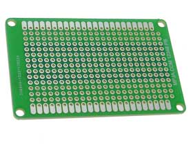
 tough matrix
I believe so
limpid nest
tough matrix
I believe so
Thx
Is this a wild thing to want? A DC to AC converter that's small and board mountable?
Low current, well under an amp
Output current
unreal flax
Are you looking to generate wall-plug AC voltages, or something else?
limpid nest
Roughly? Nothing really higher than Wall AC voltages. Really like 200-300 mA max output
I'm trying to see if I can do it reasonably and safely
I think the answer is build the circuit myself.
Which is unsatisfying but I can live with it.
I think 120 Vrms is my max
unreal flax
Yeah, I'd call that an unusual need. Though do bear in mind that even 300mA is going to be like a 40W power supply, so it's not a trivial bit of circuitry.
limpid nest
Yeah it's not small.
They make modules that are NOT board mount that I could live it
live with*
But I'd prefer something board mount
If I proceed I should probably find an expert to advise me
This doesn't exist right? I feel like I'd have heard of it. A variable resistor or resistive element that can be set digitally?
It does exist!
unreal flax
Digital potentiometer, aka digipots, yep.
limpid nest
Yeah downside is someone writing code to use a system that uses one could set a dangerous value with no safeguards
unreal flax
Note that they are typically relatively low-current devices rather than load-bearing.
limpid nest
Yeah I'd be using it in a feedback/sense application
unreal flax
If you want to bound the value to a safe range, you can put them in series with a fixed resistance too.
supple pollen
limpid nest
Is this a wild thing to want? A DC to AC converter that's small and board mounta...
Yeah, they exist. I picked up some nice 80VAC ones from a surplus outfit not long ago. You can also roll your own.
limpid nest
supple pollen
Yeah, they exist. I picked up some nice 80VAC ones from a surplus outfit not lo...
I'm looking at rolling my own
supple pollen
I've done stuff like that. For low-power, low-voltage stuff, I've been known to use a MOSFET gate driver chip as a power amplifier and optionally AC couple the output with capacitor coupling so I can bias it anywhere I like.
I'm fond of the MAX628 / TSC428 for that, as it has one inverting output and one non-inverting output, so I can use it like an H-bridge. However, there are lots of gate drivers and other amplifiers/buffers to choose from.
Another possibility is the LM4871. I found out about that one, as there was a self-oscillating VFD power supply built around the LM9022, but the '9022 was discontinued, however fans found out that the '9022 was actually just a rebadged '4871, which is still in production.
limpid nest
This would be relatively low power, but not low voltage. I need 100-120 Vrms
supple pollen
For that, you'll probably want to get step-up using a magnetic component (inductor or transformer). However, there is an EL driver chip that might suit your purpose. Want me to look up the part number?
limpid nest
If it's not an inconvenience! I'm looking at a circuit that would produce a nice sine wave out of the transformer if I can just generate two nice low voltage sine waves that are 1/2 period offset
supple pollen
Ah, like a quadrature signal? I remember the Cathode Corner oscilloscope clock uses sin/cos waves like that to draw very nice figures on the screen. For sine wave output, you may want a Royer style oscillator.
As for the EL chip, it's the Supertex HV857. Maxim also offers their MAX14514.
The SuperTex chip doesn't produce a sine wave, but sort of two sloppy half-sines
 limpid nest
I'm trying to roll my own EL wire inverter
supple pollen
Ah, so you don't need precision sine waves. It's probably worth looking at how the chip ones work, to get ideas to roll your own.
limpid nest
Chip ones?
supple pollen
The Maxim and Supertex EL driver chips I mentioned above.
One weird cool thing about EL is the color is somewhat frequency dependent, so you can change the color of the light emitted by varying the drive frequency.
limpid nest
Ahhh
Is the brightness voltage dependent?
I'd love to make a circuit that can programmatically have its brightness change
supple pollen
I think it's something like rate-of-change-of-voltage dependent (EL is sort of like a lossy capacitor, where the loss is turned into light)
limpid nest
Hmm ok. I'll start simple
supple pollen
A simple blocking oscillator in the primary of a step-up transformer is pretty simple, and should work to get started.
limpid nest
The other thing I'm trying to figure out is whether I can just switch the input to an off the shelf EL wire transformer to turn on and off
I assume I can
But I also assume being in circuit would provide better results
supple pollen
Yeah, that should be fine. Some of them offer flashing modes.
limpid nest
Yeah
I really want to make my own variable frequency variable voltage controller though
supple pollen
Here's one example of a blocking oscillator
 limpid nest
What makes the oscillation?
supple pollen
I'm with you: a source of variable frequency driving an H-bridge driving a step-up transformer would probably do the trick.
limpid nest
I know how to do the variable frequency if I can get by with a junky sine wave
If I can do variable frequency with a quadrature IC, that would be great
supple pollen
It's a blocking oscillator, so the transistor starts to turn on through leakage voltage through the 10k resistor, which induces voltage in the transformer that boosts the base drive until it's fully on. It stays that way until the transformer core saturates, at which time the voltage starts to fall, which induces the opposite voltage which kills the base drive. Lather, rinse, repeat. However, the frequency is pretty much determined by the transformer characteristics.
I'm not sure where quadrature is useful for driving EL. One big advantage of a transformer is it's easy to get differential drive out of it.
limpid nest
There's a circuit I can use that if I can generate two small DC waves, I can get one nice high voltage AC wave out
supple pollen
I'm guessing you mean two small AC waves?
limpid nest
Sorry yes, from a DC source I meant
supple pollen
After thinking about it for a while, I think a transformer is probably your best bet if you want to move to variable frequency. There are a couple of common choices. One is a small power supply transformer, run "backwards". A 10VAC out one like a Hammond 161C10 will work nicely. Another choice that was popular in the past was an 8Ω:1000Ω audio output transformer, but those are a little harder to find these days.
limpid nest
Hmmm ok thanks. I'll look at it
supple pollen
I got curious about the Maxim EL driver chip waveforms, they're even less like sine waves.
 limpid nest
supple pollen
I got curious about the Maxim EL driver chip waveforms, they're even less like s...
limpid nest
supple pollen
I got curious about the Maxim EL driver chip waveforms, they're even less like s...
It's worth trying, thanks a bunch?
Oops
A bunch!
spice turtle
I dont understand why jlpcb is having issues with this USB connector. They successfully etched it out it on one board, but they have so many questions about it on another board. Part: USB4085-GF-A 😭
has anyone ever had such an issue with JLPCB?
granite steppe
When is Via Stitching enough? Should they be close to ground connections of Capacitors and GND pins? Should they encircle positive voltages too? Is there an advantage to keep them around the edges?


 heavy jasper
I would call this probably “too much” - it’s going to make soldering a huge pain.
How many layers is the board?
And I would be more worried that despite the stitching, some of your ground returns are not as good as they could be. For instance, for your boost converter, ideally I think the VDD (input voltage) capacitor could rotate 90 degrees counterclockwise and connect via the top-layer ground pour back to the same plane as the bottom of the chip and the output (VPP) capacitors.
(I'm guessing it's a boost because it looks like the feedback resistors are on the top right; if those are VIN/UVLO lockout resistors and the feedback node is directly through the VDD connection to the lower-left then it's a buck, but the advice still pretty much applies.
granite steppe
heavy jasper
I would call this probably “too much” - it’s going to make soldering a huge pain...
It's not going to be hand soldered. Free coupons for SMT services to the rescue for me.
It's a 2 layer board, and yes, it's a boost converter.
Also, yes, that was way too many stitches. I'll scatter them better this time.
heavy jasper
If it's a 2-layer board, the advice about keeping the high-frequency loops routed back on the top layer applies even more so
granite steppe
And I see the issue of Input caps of Vdd not being in the same island of copper as the GND and that of output caps. I'll have to reposition some stuff but it looks rectifiable. Thanks.
 heavy jasper
esp. if it's a standard 1.6mm thick board - the ground plane is actually quite far away
granite steppe
4 layer is not out of reach for this board, it's small enough and I'm getting it in quantities it will pay off, yet I do not know what will I do with the second inner plane. Previously I've made the third plane as 3.3v/5v, here I don't know which will be usable. Any recommendations?
heavy jasper
You can route more than one thing on that third layer - e.g. you could route just the power connections there, even if several (and not as a plane)
granite steppe
I'm thinking I'll make copies of copper pours for Battery, USB, VDD, and Vout on the 3rd plane, and connect them to the output castellated pads/holes through those too. Given it's designed to handle upto 3Amps (Even though the battery charger can supply only 1.5A max, I'm not gonna pull any more than 1.5A), will having pours connecting enough copper to those pads make the heat dissipation any better?
 night thistle
not technically pcb specific but kinda a general electronics thing
I have this issue where parts of the circuit seem to store voltage when I'm pretty sure they shouldn't be doing that and I'm unsure how to fix it/if it's a simulator issue since they should be grounded I believe
I can share the circuit diagram if this is the relevant channel for it
supple pollen
Sounds like capacitors, which do store voltage
night thistle
the weird thing is it doesn't have any of those in the section that's holding the voltage
just a few transistors and logic gates
the relevant part is I have a transistor acting as a switch, where when voltage is applied the circuit goes to ground, but otherwise it passes through a resistor and goes to a logic gate
but the output through the resistor never loses charge which then messes up the logic stuff in turn
supple pollen
When you say "the output through the resistor never loses charge", what do you mean?
night thistle
if the circuit starts out with the transistor open and going to ground, it reads 0v through the output, but once the transistor closes and power starts going to the logic gates, it never leaves. Like even if the transistor opens again to connect everything to ground, it doesn't have the voltage drain
sorry if I'm explaining it badly I'm fairly new to the whole circuit stuff
this is what I mean by resistor output btw
 supple pollen
I'm guessing when you say "open", you mean "conducting", and when you say "closes", you mean "stops conducting". I'm also guessing the power supply comes in on the right end of the resistor, and goes to power the logic gates from the left end of the resistor.
night thistle
supple pollen
I'm guessing when you say "open", you mean "conducting", and when you say "close...
sorry for late reply but the power supply is on the left side and the logic gates are powered from the right side, other than that yes
the power supply already has a resistor connected earlier in the circuit so it doesn't short when it goes to ground
supple pollen
Ah, there's another, not shown, resistor and (for some mysterious reason) a series resistor.
night thistle
I can send the whole circuit if that would be helpful
as I said I'm not the most skilled at this so I might have made some uh
unusual design choices
supple pollen
I would agree that some of the design choices are unusual. But it seems the root problem is that once the transistor is switched off (nonconducting), it appears not to switch on (conducting, shunting the supply power to the logic) again?
night thistle
I don't think so? When I hook up a multimeter in the simulation whenever the transistor is off the voltage increases, and when it's on it stops increasing but doesn't drain to ground
any lingering voltage should still go back through the resistor and connect to ground I believe so it should still end up at 0v when the transistor switches on
supple pollen
So the voltage increases ... slowly, when the transistor is off?
night thistle
seems like it
supple pollen
With the series resistor, and some capacitance, I would expect that, assuming you're measuring the voltage on the right hand (logic) side of the resistor. It might be worth measuring it on the left (supply) side and seeing if it also rises slowly there.
night thistle
hm it does actually do the same thing on the supply side when the transistor is off but immediately equalizes if it's on
probably means something weird is going on farther in the circuit that's causing issues and I was just assuming it was an issue with the transistor switch thing
supple pollen
That would make sense, but I'll admit I'm largely guessing here.
night thistle
this is the circuit diagram I have if it's useful

thanks for trying to help me figure out what's going wrong with this btw
stuff at the bottom just drops the power down to 5v
also ignore the lack of labels I didn't know they existed until yesterday
the circuit basically checks the voltage of a 9v battery, and if it drops below 2.5V swaps to charging it, and then swaps back to draining it once it hits 8V to explain what the zener diodes are for
supple pollen
You've got a few issues there. You'll want current limiting resistors to the transistor bases, and drain resistors on the logic signals so they don't float (LS TTL has some weird characteristics when its inputs are floated)
I'm amused by the mix of LS and HC logic as well.
night thistle
supple pollen
I'm amused by the mix of LS and HC logic as well.
not sure what this means but I assume it's not a good thing
I just slapped random models of logic gates down because I haven't really used kicad too much lmao
supple pollen
It's not necessarily a bad thing, but it means you have to understand the idiosyncrasies of two different logic families, and since this is an idiosyncratic circuit, that's going to matter more than in a simple boring all-digital circuit.
night thistle
oh also is the weird thing I'm doing where I just use a signal going through two inverters as a delay considered bad practice
supple pollen
That trick is actually fairly common.
night thistle
ah alright good to know
is a drain resistor similar to a pull up/pull down resistor?
supple pollen
I would suggest adding series resistors (1k or so would likely be fine) to the connections from the zener diodes to the transistor bases, as well as shunt resistors (10k or so, maybe) from the transistor bases to ground, to absorb partial conduction of zeners near their knee voltage. I would also suggest adding shunt resistors to ground for the logic inputs driven by the transistors. For LS logic, they'll need to be fairly low value, maybe 1k or so. I don't think the series resistors are necessary.
Yeah, basically a pull-down resistor (on both the transistor bases and the logic inputs) to establish a default level.
night thistle
Alright I'll do the solutions you suggested! I completely forgot about the floating pin stuff until you mentioned it so I guess that's a likely culprit for the weird voltage retention
supple pollen
LS logic tends to float its inputs to about 3V, whereas HC is super high impedance and will float kind of randomly.
 oak token
Hi, what the best way to cut this Flex PCB: https://www.adafruit.com/product/1894 ? I've tried 60W CO2 laser cutter, it cannot cut it.

Finally, the conductive material you've known you wanted but never knew you could have, its a sheet of flex PCB material! This is the stuff used to make flexible circuits, but raw and ...
supple pollen
As always, "best" depends on your parameters. My usual approaches are tin snips or a paper shear.
Copper is very reflective to the 10.6µm CO2 laser wavelength, so that won't work very well.
oak token
supple pollen
Copper is very reflective to the 10.6µm CO2 laser wavelength, so that won't work...
Yea, that seems to be what was happening. It’s reflecting the laser. Thanks!
granite steppe
I fixed my previous design for battery charger and boost converter above. The PCB has fewer vias now and 4 layers. The second (green) layer, and fourth (blue) layer are both purely for ground. The first (red) layer has 3 ground pours, the largest at the bottom connecting the decoupling capacitors of the battery charger and boost converter together. I'd love to get any feedback for them, since due to part shortage, I only have a few days before sending it off for production and SMT assembling.


 distant raven
just a heads up, they'll charge you extra for the castellated pads and you'll need to panelize it yourself more than likely
granite steppe
I will have to remove the castellated pads for now any ways. As fun as they could be, the manufacturer does not offer SMT services for PCBs with castellated pads.
supple pollen
You may want to add some fiducials if you're planning on automated assembly.
distant raven
updated treehouse terminal which solves some hardware and usability bugs
 limpid nest
glad you started creating again 🙂
distant raven
switched to a JST PH 3 pin connector for the neopixel connector instead to a screw terminal
also removed the 1000uF through hole capacitor for a 470uF SMT electrolytic
fixed the left button hardware bug where I previously used a pin that isn't actually usable for circuitpython
everything else worked pretty well. now I can order the new version, assemble sometime in May when the TFTs arrive from Aliexpress
ordered some supervisor ICs since I ran out
distant raven
limpid nest
glad you started creating again 🙂
had to find myself again. the end of the year with family issues really stole a lot of my spirit. it's hard to find it once it's stolen
limpid nest
It can be rough, I'm fully expecting to burn out by the end of the year. We'll see how I come thru it
distant raven
just make sure you let yourself have space from it from time to time
limpid nest
Yeah I'll see what I can do
granite steppe
supple pollen
You may want to add some fiducials if you're planning on automated assembly.
Thanks for the info, bu the requirements for that are not very clear to me from the description given by the PCB fabrication service I'm using. Given that they add two or three on their own, I'll trust their judgement on that and not make extra holes which might not even be used.
 eager crescent
Yesterday, I designed my first ever PCB. It's meant to take data from several sensors and pass the data to a Raspberry Pi, which will in turn actuate pumps to control nutrient concentrations in a Hydroponic System.
However, when I took this PCB to my professor, he said it would cause a short because of the way the MCP3008 was connected using two layers. He gave me an explanation that I didn't really understand. Can someone clear this up for me?
here's the link to the fritzing file
https://drive.google.com/file/d/13ZrInxhGq75TYyru2lqztp8HxBq7bLmp/view?usp=drivesdk
Google Docs
 worldly schooner
Not sure if it’s anything your professor mentioned, but a lot of your angles traces pass fairly close to plated holes. I’m not familiar with fritzing as a pcb design tool, but if you have something equivalent to a DRC rule checker, I’d use that to confirm if that’s enough clearance for the pcb to even be manufactured…
Also, consider some bypass caps for adc stability. More info can be found in the data sheet for the mcp3008.
fervent lance
kicad vs eagle; which should a noob wanting to get more into PCB design use? i have kicad xp, but it feels clunky when trying to outline the board out line...
worldly schooner
fervent lance
kicad vs eagle; which should a noob wanting to get more into PCB design use? i h...
Kicad is trending upwards as a more popular PCB design software, but Eagle still has its advantages in regard to Autodesk integrations. One is a truly free open-source software, while the other has deeper functionality and commercial support. Ultimately, it depends on your budget and goals.
limpid nest
Yeah, if you are OK with the strict limitations of a free Fusion360 License, then that's a good choice because it can give you nice tools for designing around your board. If you can't live with the limitations and can't afford 500 dollars a year, then kiCad at least doesn't have those limitations, although it also can't do 3D work.
 amber torrent
Hello @everyone,
Is their any course or free of cost resources for understanding and learn IPC Standard for hardware/PCB design?
Kindly let me know if there is any.
Thanks 🙂
Regards
ARM
distant raven
Well, honestly.. probably not. IPC like most standards is paywalled and for the reason being that only the goodest boi companies with the financial resources to maintain IPC certification can have it
It’s not made for commoners like us
If anyone happens upon what it takes I would be interested to learn as well
Also the everyone tag doesn’t work on this server
limpid nest
I'm looking at powering one of the QT py boards from the 5V pin using a switching regulator. USB and Battery power are often smoother than a switching regulator. Is it worth it to add a 1uF MLCC cap across 5V and GND?
distant raven
Are you doing any analog work with the qt py?
limpid nest
No, just digital.
distant raven
Probably wouldn’t hurt to add a 1uF cap, might be better to do a few 0.1uF like 2-3 rather than a 1uF
Adding capacitance to the power input can cause the onboard LDO to take longer to rise so it’s probably better to keep it lower
distant raven
Usually you can apply the 5V to the 5V pin and be more than fine
Since 5V will go through the Schottky diode then to the onboard LDO
limpid nest
which I assume has filtering caps on it
that was something I was intending to look into
distant raven
5V on the QtPy is connected to VUSB before the diode so it should be fine
limpid nest
let me pull up the schematics
Yeah, there's capacitance before the LDO anyway, so it's probably fine.
If I were using like 3.3V Buck regulator to power an MCU, I'd have more concerns. But this seems fine
Hm, what does this symbol signify?
 distant raven
Test point
limpid nest
ahh thx
heavy jasper
Sometimes - and sometimes it means a power rail.
Especially given that it seems to be named as such, and possibly passing that name to the net.
(I have seen just-circle being the power rail symbol in the past)
limpid nest
Good to know, thanks!
distant raven
heavy jasper
Sometimes - and sometimes it means a power rail.
I think it’s dual purpose in the Adafruit schematics, or at least recent ones
limpid nest
Is 10% about the best tolerance you can get from a 14-15k pot? That's all I'm seeing
distant raven
I haven’t seen too many precision pots, but i think better tolerance is common on more common pot values
distant raven
limpid nest
Is 10% about the best tolerance you can get from a 14-15k pot? That's all I'm se...
Is your pot a trim or rotary?
supple pollen
Normally pots are used as voltage adjusters or dividers, where the absolute value doesn't matter very much.
distant raven
True, that explains it pretty well
limpid nest
yeah makes sense. I'm looking at digipots from adafruit now
supple pollen
You may not even need something as fancy as a digipot, if you just want a few speeds
limpid nest
I've got a few ideas I'm exploring. The digipot is complex compared to other ones.
I just have to see.
edgy jungle
Im having an issue on my PCB where I have the Ultimate GPS module. Basically it sends gps data completely fine when running alone, however when I run all the programs I dont get past this line in my CircuitPython code "uart = busio.UART(tx, rx, baudrate=9600, timeout=10)"
I even initialize it first
this is the error message when it full times out
 distant raven
edgy jungle
Im having an issue on my PCB where I have the Ultimate GPS module. Basically it ...
distant raven
edgy jungle
Im having an issue on my PCB where I have the Ultimate GPS module. Basically it ...
Seems like this could be one of two things, bad code which would probably be better for #help-with-circuitpython or it could be backwards UART traces which would be here
Could you post your PCB schematic and board files?
edgy jungle
 twilit mango
@silk lark If you're not around, don't come back for this. Your dot is green, so I figured you might be. I'm trying to figure out the difference between a breakout with the same chip in two different packages - there are images for both, and I think I figured it out, but I wanted verification from someone who actually knows these things. The first package is SOIC-8, second is HVSON. Am I right in thinking SOIC-8 has feet, and the HVSON is basically surface mount? Google is not really helping me much with this. I looked at the exact chip in both packages on Digi-Key, which is why I think it's feet vs. no feet.
 silk lark
sure
twilit mango
Basically Limor couldn't get it in one package, so she reworked the board for the other one.
silk lark
apparently hvson is also dual-inline, but with the pads under it
twilit mango
Ah ok
silk lark
original QFN had pins all around
twilit mango
The HVSON in question is pads underneath.
silk lark
twilit mango
PCF8523 is the chiup.
silk lark
twilit mango
So it's https://www.digikey.com/en/products/detail/nxp-usa-inc/PCF8523TK-1-118/2606089 (HVSON) vs https://www.digikey.com/en/products/detail/nxp-usa-inc/PCF8523T-1-118/2530422 (SOIC-8)
Order today, ships today. PCF8523TK/1,118 – Real Time Clock (RTC) IC Clock/Calendar - I²C, 2-Wire Serial 8-VDFN Exposed Pad from NXP USA Inc.. Pricing and Availability on millions of electronic components from Digi-Key Electronics.
silk lark
worldly schooner
If you need a better visualization, pages 56 and 57 of the NXP datasheet has mechanicacl drawings: https://www.nxp.com/docs/en/data-sheet/PCF8523.pdf
silk lark
it's funny how SOIC stands for "small outline integrated circuit" yet it's so huge
worldly schooner
Must have been small in comparison at one point haha
silk lark
compared to DIP: https://en.wikipedia.org/wiki/Dual_in-line_package
twilit mango
worldly schooner
If you need a better visualization, pages 56 and 57 of the NXP datasheet has mec...
Good call.
elder peak
SON I've got a million problems but keeping space for feet isn't one of them.
Now you'll never forget. 🙂
limpid nest
working on a design for which i have to make a footprint for thru hole parts. For a round post, should I make the hole exactly the diameter of the post per the part datasheet? Or like .5-1 mil wider?
distant raven
I’ve usually used a standard header sized hole which I think is 35-40mil
limpid nest
Hmm
well, for example for a .9mm post, fusion has a standard hole size that fits exactly. But for a 40mil post, I have to specify my own. I don't want to go too small, and obviously not too big heh.
and for the standard post size that fits exactly, is that what I want? or do I want a bit of clearance?
distant raven
Is this for a pot?
limpid nest
No a buck converter module
distant raven
Oh. Hmmm
limpid nest
It has 40 mil posts, a switch I'm looking at has .9mm posts
distant raven
So you could do 45mil posts so long as there is clearance between the holes
limpid nest
Yeah I figure the absolute worst case is they can't get in there. If there's some wiggle room it's not ideal, but it's far from game breaking
but what about the .9mm? Should I use the standard setting that fusion has that matches down to 5 decimal places?
At that point it's really down to tolerances from the fab
limpid nest
hmm
I'll probably just hem and haw for a while and then go with 44-45mil holes
and .95-1mm holes
limpid nest
distant raven
Right
Oh you don't happen to have a qt-py EAGLE footprint, do you? I know you do work in that space. I can make one, just feeling lazy
distant raven
limpid nest
Oh you don't happen to have a qt-py EAGLE footprint, do you? I know you do work ...
limpid nest
ha! I had a vague memory of that conversation, but couldn't find the lib anywhere! Saving it to the cloud this time. Thanks
distant raven
😬
fervent lance
Still struggling with this LED PCB design which I created. First I did the power switch wrong, so it didn't properly work on battery power. Now USB-C powered the LED project works perfectly fine, but battery powered the voltage takes at least around 20 seconds from the moment when the battery gets inserted to the project (assuming the power switch was already on ON) before it gets more stable. And even then, once I increase the power consumption (by increasing the LED brightness) to only around 600-700mA, the ESP32 reboots (guess because of the unstable voltage). Not sure if I broke the boost converter or inductor a few days ago, when I accidentally went over the 2A max they can provide (or tried to at least).
I am running out of ideas to try out with the current prototype. Maybe it's best if I just buy a boost converter and inductor with higher A ratings and integrate them into the updated PCB design, order it, assemble it and then hope it works better.
But if anyone has suggestions what might be wrong here, please let me know:o
Also by the way, charging the battery also doesn't properly work anymore with the current schematic (or at least not the way I modified my prototype by cutting traces and connecting pads with wires). And I also still wonder: can I safely assume that the battery doesn't get drained in a noticeable way, when the LED project is turned off and the battery still connected?
 distant raven
so my first critique is I'm not a big fan of how you have the battery and USB 5V input setup into the step_up_v net
There's better ways to do it that arguably make more sense, let me grab an example
this is how Adafruit does their VUSB/Battery line switching

this ends up working pretty well and helps create a definite on and off for battery usage.
that might help with the battery issues
distant raven
you might also add a supervisor IC that checks the voltage level before setting it's signal
 charred vigil
Can someone help me diagnose some issues im having with a pcb i got made
I have buttons connected to ground and an input pin on an io expander but i was having issues with the io expander so i decided to remove them from the board and just wire the buttons directly to gpio pins
the buttons are in this layout:
[0,1,2] [3,4,5] [6,7,8]
there is no continuity between any of the pins of the buttons, however for buttons 2,3 and 5,6 when either button is pressed it makes both buttons low
when button 2 or 3 is pressed 2 and 3 go low, and when 5 or 6 is pressed 5 and 6 both go low
pull up resistors are enabled on the feathers2 im using
limpid nest
Is there a quick and dirty way to do uni-directional level shifting? I'm aware of the method adafruit uses for bi-directional shifting.
 sharp crown
Level shift up? A transistor would probably work. Level shift down? Zener diode
limpid nest
Yeah, I have to figure out if a level up IC would take more space than a handful of transistors
supple pollen
The little SOT-23 single-gate level shifters are quite compact.
limpid nest
I was looking at those
Looks less headachey than dealing with a true level shifting IC.
74AHCT models in particular
I don't need MBPS
supple pollen
You can look up the ones AdaFruit uses on their ItsyBitsy boards. I vaguely recall it's a 1G125 but I'm not sure.
limpid nest
I recall from the last time I did this, I actually need 4 channels so the 4 channel variant of the AHCT is perfect
fervent lance
distant raven
you might also add a supervisor IC that checks the voltage level before setting ...
any suggestions on how to find such an IC? what keywords I need to look out fot?
fervent lance
distant raven
this is how Adafruit does their VUSB/Battery line switching
ah yeah good point. But I would still need to adapt it, since I also have the physical power on/off switch, which is supposed to tun on/off power (/the boost converter).
Also, shouldn't there also be a diode protecting VBAT from VBUS?
fervent lance
fervent lance
ah yeah good point. But I would still need to adapt it, since I also have the ph...
actually, never mind that last part. MOSFET have the internal diode...
fervent lance
distant raven
this is how Adafruit does their VUSB/Battery line switching
I am still confused by how MOSFETs work honestly... and which MOSFET (P or N) to use... but just so I understand it right - Adafruit uses a P channel MOSFET here, right?
distant raven
fervent lance
I am still confused by how MOSFETs work honestly... and which MOSFET (P or N) to...
Yeah, so in this case Adafruit is using the mosfet for two purposes.
- When VUSB is ON, it acts as a diode since it turns the mosfet off.
- When VUSB is off, the mosfet gate is saturated making it act like a resistor.
It’s not necessarily used in the way you might expect, but it’s very effective.
As for a supervisor IC, you want one that has a rise time similar to the largest rise time for your regulator
supple pollen
The nice thing about the MOSFET versus a diode is the lower voltage drop when it's on. This is why the MOSFET is in the lower voltage (battery) supply. The voltage drop of the diode in the USB supply doesn't matter (I think it's a Schottky diode, so the diode drop is low anyway).
fervent lance
distant raven
As for a supervisor IC, you want one that has a rise time similar to the largest...
still recommended, despite the battery management chips already being integrated?
distant raven
fervent lance
still recommended, despite the battery management chips already being integrated...
I’m not sure what you mean. Unless your BMIC is sending an enable signal to your voltage regulator you likely still need a supervisor if your battery operation is causing delayed rises in operating voltage for your other components
fervent lance
still not sure I understand what the IC is supposed to do. Cutting off the battery connection if it goes under a minimum voltage level?