#help-with-hw-design
1 messages · Page 61 of 1
 limpid nest
 cinder anchor
Hmm, cool, so how do I do that in KiCad?
is this a good tutorial? https://www.wayneandlayne.com/blog/2013/02/26/kicad-tutorial-copper-pours-fills/
Do I just add rectangles and such directly on the copper layer?
limpid nest
No idea, I'm a fusion man
cinder anchor
lol
how do you do it in Fusion/EAGLE?
People keep telling me to go to KiCad, but nobody knows how to use it. I sense a trap.
limpid nest
Uuuuuuhhh I'm away from my PC but there are a bunch of tutorials.
limpid nest
Np
 unique flare
How on earth do I create a footprint for these pads? I've shared the photo of the board & the measurements according to it's datasheet.


Is this correct? (have since changed the shape from "Custom (Rect. Anchor)" to just "Rectangular" without any visual change)
 limpid nest
unique flare
How on earth do I create a footprint for these pads? I've shared the photo of th...
limpid nest
unique flare
How on earth do I create a footprint for these pads? I've shared the photo of th...
Carefully :)
cinder anchor
 distant raven
Is the NM necromancer?
distant raven
Is the NM necromancer?
Lol, no, Nascent Maker. It's what I go by on 3D printing sites and such. Don't need any attention from employers there in case I decide to remix something unsavory, like a weed grinder or something.
cinder anchor
limpid nest
Uuuuuuhhh I'm away from my PC but there are a bunch of tutorials.
Does that look better?

here's a better view if you wanna zoom
I don't think it liked my filename... uhh
uh yeah... definitely didn't like the word ||fat||
I am pretty sure it put me in Discord jail for like 5 minutes, too. Weird. ¯_(ツ)_/¯
limpid nest
What are the big yellow traces from J1, J2, etc?
limpid nest
Sorry what signal?
cinder anchor
Not ground and not data. The other one.
limpid nest
12V?
cinder anchor
Yeah.
limpid nest
I'd do that in a polygon too if you can
Assuming they all come from the same 12V source
cinder anchor
They do come from the same source. Why isn't the traces enough?
limpid nest
I mean it's probably fine but a big polygon is better
cinder anchor
Is it like 2 hours worth of work better, or just prettier because?
cinder anchor
the traces are 2 mm wide, so according to the calculator in KiCad, that's gonna be about 3.95301 A at 10 AT (I can't make the funny triangle, so just imagine that A has no legs!) with a trace thickness (H) of 0.035 mm.
limpid nest
Yeah they are probably fine
cinder anchor
Otherwise I'll have to reroute a bunch of stuff. Hmm. What if we make them thicker?
is that an option with OSH Park?
limpid nest
Not sure, don't think so. JLC can. But keep on mind that it makes soldering harder in general
Also when you make these, make more than one so if one randomly goes bad, you have a spare


 limpid nest
I'd do a bigger ground pour (always a good thing) and put it on the bottom
cinder anchor
 cinder anchor
limpid nest
I'd do a bigger ground pour (always a good thing) and put it on the bottom
cinder anchor
limpid nest
I'd do a bigger ground pour (always a good thing) and put it on the bottom

bottom looks like that
limpid nest
2Oz copper is gonna be tough for a novice solderer fyi
You can also do ranked polygons
So two polygons occupy the same space and one carves out the other
cinder anchor
sure, and there's exclusion zones as well, which I tried, and they work in a similar fashion for clearing out things around an area
2 oz copper, not 20
and why is that harder to solder?
cinder anchor
I don't even know how thick they are on that Sparkfun board...
cinder anchor
they're outputs
J7 is the only input
the others are for connecting things like the fridge, flood lights, and such...
so that they can be turned on and off with the RP2040
limpid nest
Ahhh
cinder anchor
Did I wire them correctly?
limpid nest
Let me check can you post a PDF of the schematic?
limpid nest
So
Reason I thought those were 12V inputs is you are doing low side switching here.
nevermind, I see
is j7 your 12V input? You might want to work up a more descriptive silkscreen
limpid nest
I might actually suggest a barrel jack there
cinder anchor
but it's going to come off of a busbar from the battery
limpid nest
ooh nevermind, you've got cable glands going on
limpid nest
I'd say +12V Input at one terminal and GND on the other terminal
cinder anchor
cool
I shouldn't edit the reference, right? Just add stuff directly on the silkscreen?
limpid nest
Yup
cinder anchor
I'll keep the references on the silkscreen but inside the outlines for the screw terminals, that way I can sort things correctly when assembling and looking on the schematic
limpid nest
nice
cinder anchor
they just won't show once the terminal is on top
limpid nest
I'd have them showing, the idea is to make it easy to put the wires in the right spot when 6 months have passed, you're on the road, and don't have KiCad around
cinder anchor
Good idea. I think I'll just label them "12V OUT" 1..6
that way I can label the cables with the number so I know which one is connected to what
cinder anchor
ooh yeah
 tough matrix
@cinder anchor I forgot - what current are you planning for?
cinder anchor
tough matrix
<@!438791522285256715> I forgot - what current are you planning for?
12 V @ max 4-7 A.
Fridge will draw max 4.5 A if it's set to max.
tough matrix
well, for 4-7A, you can do with 1oz copper
cinder anchor
So I don't need double copper?
tough matrix
it would be nice to have it, of course, but is is much more expensive. 60mil trace is quite adequate for 4.5A
in 1oz copper
cinder anchor
But, if I went up to 2 oz, would that be better?
tough matrix
yes
cinder anchor
So, I think it's the same price.
distant raven
When it doubt 2oz
tough matrix
if money is not an issue
distant raven
Slightly more but worth the cost if you’re unsure
 tough matrix
if so, go for it
cinder anchor
cool, just gotta make sure the board is sound first
so any help appreciated before I waste $40
cinder anchor
Hmm. I don't know.
tough matrix
is there a reason you chose 0.8?
tough matrix
doesn't really matter for your design
cinder anchor
Would the thickness of the board have any real impact where GND and +12V overlap on bottom/top layer? Will it do anything to the P0-5 digital signals from the IC?
tough matrix
no
cinder anchor
here's a clearer image of the traces
tough matrix
i2c is slow
cinder anchor
yeah, this is just for turning on and off MOSFETs, so probably not impacting anything?
tough matrix
for USB, it is suggested to have GND pour under the D+ and D- traces, and thinner board is better
cinder anchor
should I have GND pour under the JST SH Qwiic port?
actually, it already comes with paste for the MT slots
tough matrix
nah, for I2c it is not important
cinder anchor
cool, ok
tough matrix
the board looks fine to me - I assume you ran DRC
cinder anchor
DRC came back clean.
What do you think of the board? Will it work? And, will it work in a way that doesn't break anything, like a really expensive 12 V battery? Will it set stuff on fire?
tough matrix
normally people put qwiic connectors on the edge of the board; yours is some distance away from teh edge
cinder anchor
should I move it out?
cinder anchor
you think I need to move C1 up with the QT port, or will that short distance be fine?
I have a feeling I should move it up
cinder anchor
tough matrix
can you also show the scehmatics? not the board but the schematics?
sorry, other file should have been named pcb
Also, I embarked on this journey because I didn't want to pay $950 for an sPod controller. I've probably spent at least that on components for this thing, in iterations, as I've been exploring. But, I have learned a lot of things.
tough matrix
"Why pay $20 for something when you can build it yourself - after spending $100 on parts and tools"
cinder anchor
And this way it also connects directly into the DC-DC charger and Solar MPPT Controller for some pretty awesome stats.
tough matrix
that goes for all of us
cinder anchor
lol
cinder anchor
if I built it fresh, with parts I bought right now, including the boards, I am pretty sure it's below $300, including the enclosure.
cinder anchor
tough matrix
so what are you switching?
One of these: https://icecofreezer.com/collections/iceco-vl-series/products/vlpro45s-12v-refrigerator

www.icecofreezer.com
ICECO new model Series VLpro portable refrigerator, refrigerator 12v. A versatile lid electric cooler that can open the car fridge from each side. Best for your RV, truck, outdoor living. 110/240 AC cooler for home use, 12/24 camping fridge for car.
0.715kw/24h no load in Max mode running at 0F
tough matrix
One thign I would certainly add is bulk capacitors
tough matrix
at power input
cinder anchor
OK, can you help me figure out how to do that?
Other than the fridge, it's only going to be lights that are connected to the other ports, mostly.
tough matrix
just get a couple of 470uF /25V caps and place them on the board close to J7 screw terminal
between 12V signal and GND signal
cinder anchor
I just ordered some of these:

But, I think my order is still in exception, so maybe Sparkfun has some, lemme check
Where do they go? On power or GND?
tough matrix
between power and GND
cinder anchor
is this too chonky? https://www.sparkfun.com/products/8982

Electrolytic decoupling capacitors 1000uF/25V. These capacitors are great transient/surge suppressors and work well in high-voltage and audio applications.
tough matrix
would work, if size is not a problem
tough matrix
wow
cinder anchor
it's going to house a few buttons and a display
but other than that, there's going to be tons of space inside
some fuses, but yeah
I am wiring the fuses outside of this, right, between these outputs and the fridge and lights?
tough matrix
also, I haven't done any computations, but ti may be that that the MOSFETS produce enough heat that you will need heatsinks
cinder anchor
You talking about the MOSFETs?
tough matrix
yes, sorry
cinder anchor
Or the decouplers?
cinder anchor
I have heat sinks for the MOSFETs.
tough matrix
good
final thing, screw terminals
I generally dislike them, but they are indeed the easiest way of connecting mid-power outputs
cinder anchor
I like the latching terminals too
I ordered these, though: https://www.adafruit.com/product/724

Nothing makes a project harder to maintain than a lot of loose wiring. That's why we like to use terminal blocks whenever making PCB-to-Wire connections. These particular 3.5mm terminal ...
tough matrix
two things about them:
- you are very stroingly advised to use ferrules with screw terminals
cinder anchor
what does that mean?
So, should I switch to a different type of terminal?
Just tell me what to use. 😄
tough matrix
cinder anchor
aaaah I see
tough matrix
this is a way of keeping all strands of stranded wire together
and no, tinning the end of wire before inserting it in the terminal is NOT the right way to do it
cinder anchor
I have some of these on order: https://www.sparkfun.com/products/15900

Latch Terminal 5mm pitch, 4-pin. Rated up to 250V @ 11A and can accept 18-22AWG wire.
but, they'd have the same issue, right?
So, can I go with some kind of lug terminals?
with rings?
tough matrix
these are too large
cinder anchor
yeah, the latch terminals are huge
limpid nest
cinder anchor
aaaah I see
They may make your cable glands impossible
cinder anchor
limpid nest
They may make your cable glands impossible
what makes the cable glands impossible?
cinder anchor
Why?
limpid nest
Size
Not guaranteed but they may. You can also use solid wire and ferrules aren't really necessary, IMO
tough matrix
with solid wire, sure
cinder anchor
K. I think the glands I have expand pretty big.
limpid nest
Just make sure
cinder anchor
yup
tough matrix
second thing about screw terminals I wanted to say is that they are not all created equal. The cheaper one have kind of flexible metal "leaf" and the screw pushes on it from above. More expensive ones are "rising cage" type.
both will work, but if you expect the wire to be pulled on or wiggled regularly, the "rising cage" ones are more reliable - less danger that the wire will get loose
in your case, if the wire goes through cable gland to outside, it is probably not much of an issue
cinder anchor
ok
 crude ocean
I've seen a 3d printer that has some really thin slippy 120V non solid wires going to the PSU terminals, worries me a ton and a half
tough matrix
yeah... 120V is not something you want to short
cinder anchor
yipes
@tough matrix what's your verdict, ditch the screw terminals and replace with latch terminals?
tough matrix
I'd keep them. But get ferrules for your wires
cinder anchor
cool deal, will do
and do I need to do any ground pours on the middle terminals of the MOSFETs, or are those traces wide enough once they're 2 oz copper?
tough matrix
they are dirt cheap on amazon, but you need a crimping tool - another $15
cinder anchor
I've got several different crimping tools, I think I have one that will work
been slowly getting tools and things for birthdays and Christmas, and I've built up a budget electronics lab over like 3 years
and I am now ready to rock and roll
what is 2 oz copper in mm height?
is this the right unit?

if so, no need to answer what 2 oz is in mm, lol
and those 2 mm wide traces at 2 oz will handle 6.45 A
so maybe not take any chances and do ground pours?
tough matrix
2mm traces at 2oz should handle 6.5 A easily
note that this is for 10C temperature rise. So if you feed it 7A, worst thing that happens is that temperature will rise not by 10C, but by 11C.
ok, bedtime here.. good night
cinder anchor
cool thanks for the help!
Lights I am getting will be a pair of these: https://www.4wheelparts.com/p/rigid-industries-d-series-pro-flood-surface-mount-led-light-pods-202113/_/R-FLWB-202113
they've got an amp draw of 2.14
I don't see needing any more than those, so with the fridge on max that's a total of 4.5+2.14=6.64 A.
Only other thing I would want is to be able to charge camera batteries and drone batteries, so adding a couple of USB ports at 2.4 A. That brings the total to around 10 amps, right?
So, if charging via USB, and keeping heat down means I turn off the floods, then so be it.
But, I am probably just going to run a 12 V to a receptacle in the enclosure, so no need for USB on the board itself
we'll see tomorrow what the verdict is ¯_(ツ)_/¯
cinder anchor
@tough matrix @limpid nest I have updated the board, not sure if this is better? Please let me know what you think...
unique flare
limpid nest
Carefully :)
it took me hours, but I did it 
 inland jungle
anyone have opinions of good cable-to-board connectors? .1" headers aren't quite secure enough. some combination of inexpensive, secure, and available for pin counts of 2-5 or so
 unique patio
inland jungle
anyone have opinions of good cable-to-board connectors? .1" headers aren't quite...
unique patio
inland jungle
anyone have opinions of good cable-to-board connectors? .1" headers aren't quite...
We use JST SH and PH a lot. They are quite tight-fitting.
 mental relic
JST connectors are really quite good for secure wire to board connections
unique patio
The "STEMMA/QT" connectors are JST SH.
inland jungle
yeah, I've made some PCB board with those to fit into the STEMMA ecosystem. A bit tricky to make your own custom cables though
 elder peak
I mean at that point, screw terminals.
unique patio
yes, we stock a lot of jumper combos for that reason
mental relic
Agreed, especially with short pitch connectors
limpid nest
Samtec has some great options. Pricey but effective
elder peak
You can get some connector types pre-crimped from Digikey with just the wire and the terminal to make custom cables, but not everything.
And crimping at home... well, it just puts a crimp on my style.
mental relic
Crimping at home is something of a gamble, TBH
inland jungle
Thx guys. Screw terminals might be the answer for some applications and I'll check out some of the other suggetions
 heavy jasper
DB connectors are also decent for this because they often come with solder cup options.
(Or any other connector with solder cups; switchcraft makes a bunch).
A bit delicate to solder, but gives you a pluggable connector without needing to do crimping. My general philosophy on crimping is “do it with the right tool, or not at all” and unfortunately crimp tools (aka hand applicators) can be quite expensive.
limpid nest
heavy jasper
A bit delicate to solder, but gives you a pluggable connector without needing to...
Indeed. I'm doing solder cup for a design for this reason. The crimp tool for the connector is like 700 dollars.
inland jungle
yeah, panel mount DBs for the box with internal wiring to the PCBs is a decent option
limpid nest
inland jungle
yeah, panel mount DBs for the box with internal wiring to the PCBs is a decent o...
How many connections are you making?
inland jungle
I'm wiring up a variety of sensors, buttons, and I/O for driving steppers, so anywhere from 6 - 10 outputs per board, right now using QTPY 2040 with breakout headers
limpid nest
ah OK
for your DB-board connector I'd recommend Samtec again. They aren't cheap per-connector but they are among the best quality and quite configurable.
 mossy acorn
Would it be possible/worth looking into creating a PCB "whip antenna" for 433Mhz frequency? I want to try keep my footprint as small as possible for my project, so I'm thinking including an antenna on the bottom layer of my PCB will reduce total space required instead of using an external wire/uFL antenna. Is this even feasible?
https://learn.adafruit.com/adafruit-feather-m0-radio-with-lora-radio-module/antenna-options (my project is based on) states that a whip antenna would need to be approx. 6.5 inches, or 16.5 cm @ 433Mhz. I'm unsure if the angles required to fit such length of copper trace in my target PCB footprint size would affect the efficiency of the antenna at all
 unreal flax
You might also look into helical antennas.
mossy acorn
unreal flax
You might also look into helical antennas.
I did come across those while looking at some other products, this might be the best approach I should take in this case.
I know nothing about how RF/Antennas work, so I just assumed I could make the same length copper trace as the "whip antenna" wire length, but I don't think this is the case
unreal flax
Being embedded in the FR4 dielectric material would probably affect things, yeah.
There's a fair amount of "black magic" in RF board design, so it's not generally something you can just wing and get right the first time.
You'd want to work from a known-good reference design, ideally, if you want to go down that path.
mossy acorn
unreal flax
There's a fair amount of "black magic" in RF board design, so it's not generally...
This is essentially what I need, I think I'm gonna look into a helical antenna 😆
Thank you
 magic quest
hii everyone
so im looking to do this project
but im not sure about how the heating thing works
can someone help me with this project?
 proper anvil
magic quest
can someone help me with this project?
proper anvil
magic quest
can someone help me with this project?
you're more likely to get a useful response the more information/specific of a question you can give, by the way
just from looking at the site, it mentions a heater cartridge of some sort, so I imagine there's a resistive heater embedded in the aluminum tube holder/heatsink. im not sure if this answers your question though?
magic quest
@proper anvilthere is no resistor that it uses
all the components are smd components
and when i looked at the ppcb files there was something like this

so i have to machine this part out of aluminum ?
as in the final product it shows it is of aluminum
but there are no cad files for this
only pcb files
@proper anvilsee this
while the part tha holds the tube has the file and material and size in a different folder call d parts
this is the part that will hold the tubes
proper anvil
magic quest
<@!320634828594741249>there is no resistor that it uses
you dont have to ping multiple times,
that looks like a resistive PCB heater. it heats up because the trace is extremely long and thin, thus has a high resistance. you would need to get that PCB manufactured
magic quest
im sorry as im very new to hte computer aided design and pcb making hting
proper anvil
and then I presume the aluminum heatsink sits on top of that to spread the heat.
magic quest
proper anvil
you dont have to ping multiple times,
that looks like a resistive PCB heater. it...
ohh
so i just send the gerber file to the pcb maker
and they will do all the thing?
or i have to tell the shop wha to do
proper anvil
Assuming that PocketPCR provides the gerber file, yes that should work
but they won't make you the aluminum heatsink, that you need to procure somehow else
magic quest
yes all files are there
the entire project is opensource with schematics and design and code
magic quest
proper anvil
but they won't make you the aluminum heatsink, that you need to procure somehow ...
so i give the heating thing to a pcb maker and alumium tube holder to a cnc shop right?
proper anvil
yeah it looks like a very good project. I'm really interested in their digital microfluidics product but I dont have $1200 laying around for it
magic quest
oh
proper anvil
magic quest
so i give the heating thing to a pcb maker and alumium tube holder to a cnc shop...
Sounds like a plan
proper anvil
Depending on your location, there may be shops around where you can upload the CAD file online to get a quote, or you can call/email a nearby shop and ask about it.
magic quest
and will just be a wire
magic quest
proper anvil
Depending on your location, there may be shops around where you can upload the C...
ye i have a contact that told me they can help me wiht this thing
i was not sure wether to gibve the pcb files to cnc or pcb maker
proper anvil
Looking closer, it looks like they actually use an aluminum PCB instead of FR4
magic quest
also just asking htis to be sure the gerber files will have all the info on how to make it ?
or ill have to tell them the material to use?
magic quest
proper anvil
Looking closer, it looks like they actually use an aluminum PCB instead of FR4
im not sure howit is

 magic quest
this is theri instruction manual but the kit has all the thing assembled
i didnt know aluminum can be used to make pcb
proper anvil
Yeah im not sure, they don't provide much in the way of instructions for DIY as far as I can find
magic quest
ye
proper anvil
 magic quest
😦
proper anvil
Here you can see what looks like FR4 of that same PCB, but if the aluminum part they have is not different from the one in the github, it could be a stack of aluminum on fr4?
magic quest
yea
wait

here is the pcb that i opened in a viewer
kicad is the program i used
proper anvil
Yeah so that'd be the base, and then in either case (FR4 or aluminum) the heater PCB gets stacked on top of that main board
proper anvil
Oh wait, I'm pretty sure we're just looking at black solder mask printed onto an aluminum PCB.
magic quest
same for the lid
magic quest
proper anvil
Oh wait, I'm pretty sure we're just looking at black solder mask printed onto an...
idk what it is
i can show the back side
proper anvil
Is the back side blank?
magic quest
 proper anvil
of the heater pcb


 proper anvil
I'm like 75% sure that we're looking at an aluminum PCB with black soldermask on the bottom but not the top, but I'd wait for someone else to check me.
There are PCB manufacturers that can make your PCB out of aluminum, you'll have to shop around to find one. JLCPCB is one. I don't think there are any components on the heater board so you won't have to pay for assembly on that one, just give them the gerber file.
magic quest
oh i see
proper anvil
Thats interesting because it looks like the lid is a PCB heater as well, but doesn't seem to be wired up. I guess they planned to heat from both sides but decided only the bottom.
proper anvil
magic quest
jlcpcb shows 60 usd for shipping xD
if you jsut did the quick quote, it defaults to the most express option they have
I am located in the states and the cheapest shipping option for me is <$5
magic quest
proper anvil
Thats interesting because it looks like the lid is a PCB heater as well, but doe...
ye same here as they mention on the website that ther device does not have heated lid and so we provide mineral oil
magic quest
proper anvil
if you jsut did the quick quote, it defaults to the most express option they hav...
oh
 lyric whale
Hello hello. I'm looking for an EE to help iterate a PCB designed in Diptrace, utilizing arduino. This is a paid thing. More info here. And, apologies if I'm posting to the wrong place! https://www.nyarts.org/ee-needed/
unique patio
lyric whale
Hello hello. I'm looking for an EE to help iterate a PCB designed in Diptrace, u...
Find maker jobs in 3D and CAD, Art, Design, Education, Embedded Development, Engineering, Fabrication, Marketing and Communications, and Web Development
lyric whale
Thanks @unique patio !
 hollow steeple
If the datasheet for an IC (BU97950AFUV) states that it needs no external components, but later states that one power line (VLCD) needs to power up after VDD and power down before VDD, that seems like it would require external components. Odds on just chancing powering them from the same line?
unreal flax
For what it's worth, I've generally had success in ignoring power-sequencing requirements. It's not the sort of thing you'd want to skip in a highly-reliable commercial product design, but for hobbyist hacking, it's a corner you can often cut.
hollow steeple
Ok, that lines up with my completely uninformed sentiment. I did start to lay out the PCB with spot for a voltage sequencer but even that I can only figure out how to do power up. I figure if the problem is weird output (it's a large LED segment controller) on boot I can live with that.
Unrelated: If I'm using a p-channel mosfet to control the power source for battery + usb (like the feathers), does it make sense to run through another p-channel mosfet to add a low-power physical switch?
limpid nest
hmm running into an unexpected issue. I was hoping to use an AW9523 as a low side switch to control Solid State Relays. But it's not working with my test relay. It seems to me like it should work just fine?
This chip would have been really nice to use since it's tiny and can do double duty as a GPIO expander
ooh there's some hope! The relay doesn't fire with straight 3.3V across it either.
So maybe it's not my understanding of electronics
heavy jasper
Is the relay specified to close at 3.3V? That’d be an awfully low-voltage relay.
limpid nest
3-15
limpid nest
sensata crydom ED24D3R
I'm trying my other test relay to see if the first was bad for some reason
hmmm not firing either
I solved it
my 3.3V supply is sagging a TON
down to 2.3V
PSA to anyone here, do not buy cheap stuff
anyone have a breadboard friendly power supply they like? I'm in the market for a benchtop supply too but that'll have to wait for a bit.
limpid nest
heavy jasper
Which relay?
dang, I swapped the supply for one that reads 3.288V but the relay still isn't tripping. Any ideas?
nevermind, bad connection! Woof, this has been a bad prototyping experience
cinder anchor
Hey, @ember laurel! I have been playing around with the JLC/LCSC stuff, and it's pretty neat. I have one little problem. I don't like their online editor, and I was wondering what do you do for footprints and such when you design PCBs for JLCPCB purposes? I know you gotta include some custom fields, and so far I've been adding them manually, like the peasants do.
Are there any libraries out there I can tap into?
I prefer to wear a white hat, but I am not opposed to writing a JavaScript plugin for Chrome that just scrapes them out of the editor. 😄
 sweet inlet
Howdy
I broke the locking tab on a molex kk connector -- is it possible to replace the plastic housing without soldering?
This is a nice to have, mostly to satisfy my own ocd, I'd like to change the plastic housing.
heavy jasper
I doubt they molded metal locking tabs into the plastic - you should be able to just pull the entire plastic housing off the board (warming it up to not-solder-melting-point can help to loosen the plastic). Then get a fresh connector, and use some pliers to pull the pins out of it one at a time, and press fit the replacement plastic onto your original board header.
sweet inlet
thanks!
 ember laurel
cinder anchor
Hey, <@!728007183673065614>! I have been playing around with the JLC/LCSC stuff,...
ember laurel
cinder anchor
Hey, <@!728007183673065614>! I have been playing around with the JLC/LCSC stuff,...
You can use any of your favorite PCB tools (KiCad, Altium, Eagle) and just upload Gerbers, NC drill and Pick-N-Place files.
good news from my side - I'll be getting the first orders for our product this week - Initial batch of 500 units. Excited to start production!
 flat nimbus
want to make some PCBs but lack experience. how much does it cost typically do do prototype runs? think silkscreened badge style
 twilit mango
flat nimbus
want to make some PCBs but lack experience. how much does it cost typically do d...
twilit mango
flat nimbus
want to make some PCBs but lack experience. how much does it cost typically do d...
How many boards do you consider to be a "prototype run"?
flat nimbus
10?
5?
i'm assuming the first batch will need to be redone
hoping to do transparency btw
twilit mango
Not sure about transparency, but places like OSHPark do small runs priced based on size of the board. I don't know the pricing off the top of my head, but I'm sure it's on their site. Digi-Key does the same. There may be others, but those are the two we deal with for protos. So you can do 6 boards or something for $x and pay based on the total size of the boards.
flat nimbus
this is what i'm talking about
 twilit mango
From OSHPark: $5 per square inch, per set of 3 for basic prototypes.
flat nimbus
ok, that's very doable
twilit mango
Price goes up from there depending on other factors, like speed of return and thinner boards and so on.
flat nimbus
ok
i guess i will be trying to prototype the shape shortly in fusion 360
thank you for supporting this community, @twilit mango
twilit mango
You're quite welcome! Thanks for being a part of it!
cinder anchor
When I run ERC on my schematic in KiCAD I get the following error:

How do I address these?
I am using the standard +12V, +3V3, and GND symbols.
unreal flax
Well, where is your board getting 12V power from?
unreal flax
How does the battery connect to the board?
cinder anchor
Through screw terminal J8
 unreal flax
Cool, so you'd want to mark that pin 2 as an output power pin, since it's the source of 12V power from your board's perspective.
cinder anchor
Nice, one question, what's the best way of doing that in KiCAD without editing the symbol, because when I did, ERC flagged it as edited. Should I make a copy in my project symbol library?
Or is there some shortcut?
unreal flax
I'll let someone else chime on that, since I'm mostly an Eagle user instead of Kicad.
cinder anchor
Thank you for the assist!
cinder anchor
Figured it out! It was a bit weird. So, in order to do it:
- export the
power:+12Vsymbol to a new symbol library - assign it to project
- edit the symbol in your new library
- edit the pin and add alternate pin definition with electrical type set to output
- save the library
- replace all +12V symbols on your schematic with the new symbol
- edit the output symbol by going to alternate pin assignments and click on the alternate assignment column (it's a select field) and select the alternate pin
- profit
(if you edit the symbol on the schematic, ERC will continue to complain about it, hence why I exported to a new library and added that to the project)
unique flare
https://www.zedlabz.com/products/noise-filter-for-game-boy-advance-power-cleaner-flex-ribbon-cable-nintendo-gba-easy-install-capacitor-mod-for-ips-lipo-audio-noise-reduction-5-pack-zedlabz
How are the solder points designed on these?

ZedLabz
Features:- Easy install flex cable for Game Boy Advance noise reduction.- Perfect for modded consoles with IPS screens & or battery mods.- Three solder points on ribbon mounts flex cable to the motherboard.- The tiny Capacitors pre-installed onto the flex cable.- Requires console disassembly and soldering to install.Description:The installation ...
cinder anchor
Does anybody know if there's a part in JLCPCB for the JST SH STEMMA/QT/QWIIC 4-pin connector?
https://www.adafruit.com/product/4208
is this the same style connector?
https://www.digikey.com/en/products/detail/jst-sales-america-inc/BM04B-SRSS-TB-LF-SN/926861
Is this the right part?

 bright thistle
flat nimbus
this is what i'm talking about
bright thistle
flat nimbus
this is what i'm talking about
How odd, now I crave for potatoes...
@flat nimbus, depending on where you live, the size of the board, and don't mind having plain green PCBs, you might consider Aisler as well for manufacturing.
Either way, both will bill you for the smallest rectangle containing your design (they don't charge for the effective area)
Example: a ø10cm circular board will not be billed for 78cm², but for 100cm² instead, as it'll be cut out from a 10cm×10cm square
If you need more exotic features, you may try jlpcb, but cost rise up really fast if you select less common stuff, like coloured PCBs. Also, shipping from China
Oshp and Aisler bill for a minimum of 3 pieces, jlcpb bills for 5, IIRC
magic quest
hii
anyoen knows how to use the schematic to make a new pcb?
im doong a project that has given the pcb files along with schemaics but the given files are for smd and those components are not available here (some are some arent or not of cirrect footprint)
so i want to make my own tht version of the pcb and use tht components but whereever i tried to search for converting smd pcb to tht i got opposite results (converting tht to smd versions)
also when i open the given schematic file (kicad) and try to make new pcb by clicking to switch to pcb it opens the given smd pcb file and wont allow me to make a new pcb
 worldly schooner
cinder anchor
Does anybody know if there's a part in JLCPCB for the JST SH STEMMA/QT/QWIIC 4-p...
worldly schooner
cinder anchor
Does anybody know if there's a part in JLCPCB for the JST SH STEMMA/QT/QWIIC 4-p...
JLCPCB has the original under the number C160390, but there's only 3 in stock. As far as I know, all of the 1.0mm pitch headers should be JST SH-compatible clones, with varying degrees of quality. I don't think there's any alternate style for that pitch that's common for wire-to-board...
cinder anchor
worldly schooner
JLCPCB has the original under the number `C160390`, but there's only 3 in stock....
Thank you.
tough matrix
cinder anchor
Does anybody know if there's a part in JLCPCB for the JST SH STEMMA/QT/QWIIC 4-p...
I used this clone - it is indeed equivalent to genuine JST SH4 and works just fine with regular qwiic cables.
https://lcsc.com/product-detail/Wire-To-Board-Wire-To-Wire-Connector_BOOMELE-Boom-Precision-Elec-C145956_C145956.html
BOOMELE(Boom Precision Elec) BOOMELE(Boom Precision Elec) C145956 US$0.0734
LCSC electronic components online Connectors Wire To Board / Wire To Wire Connector
- leaded datasheet+inventory and pricing
cinder anchor
Thanks, @tough matrix.
 rigid raft
does anyone know of any good buck-boost converters? I can't find any in stock that fit my needs
the input range is 3V to 11V, output should be 5V or 3.3V (I can deal with either). output current is 1 to 2A.
something like Texas Instruments' TPS series chips, except actually in stock in 2022 lol
unreal flax
rigid raft
does anyone know of any good buck-boost converters? I can't find any in stock th...
I haven't used this before, but it's in stock and seems to meet your needs: https://www.digikey.com/en/products/detail/monolithic-power-systems-inc/MP28167GQ-A-Z/15839031
rigid raft
oh nice! I've never used any MP parts before, are they reputable?
I am heavily biased towards TI lol
unreal flax
Yes, I'd say MPS is reasonably well-regarded. I use a lot of TI too, so I sympathize with that default option, heh heh.
rigid raft
thank you very much 🙂
I've never seen these I2C chips before, is that something required for operation?
(I can read the datasheet but if you know off the top of your head, saves me some time :P)
unreal flax
It doesn't look like it's required offhand, since it also has a feedback pin to set the voltage with a resistor divider. But it looks like you can dynamically change the feedback target voltage to do software voltage changes if you need it, too. Cute.
rigid raft
Ah I just saw that haha. that's pretty neat though.
I'm gonna bookmark this for a later project too
I think i found out that the buck converter I was using is actually sufficient - I think I found an issue with my design that is sucking up more power than I think it should
unreal flax
I think they also have fixed-output chips in the same series if you don't want to fool with the adjustability.
rigid raft
I took the speaker off of the circuit and it dropped 500mA lol
Yep - I was passing DC through the speaker. 100uf cleaned it up
Still gonna keep this on the radar though, thanks so much
unique flare
Can you create ribbon-cable connectors on a flexible PCB?
I'm wanting to connect two separate flexible pcbs together with something like a ZIF
unique flare
Ok... well it's totally possible because I'm finding things like this
 heavy jasper
Yes, absolutely - in fact the flat-flex cable assemblies are just flexible PCBs.
unique flare
That's what I thought. I'm trying to find some options for zif connectors
heavy jasper
Many of them are “close to ZIF” in that they have separate latching that applies the pressure - because the tips of the connectors are delicate by their nature you generally can’t just shove them in super well.
Some vendors that come to mind are Hirose, Amphenol, and Samtec
unique flare
Ahh, that'd be perfect and tbh what i was envisioning
cinder anchor
Hi folks, I have made some updates to my board, and I think it's in better shape now. I misunderstood some stuff and didn't isolate the IC from 12 V, that's taken care of now. Please let me know if you think this can be sent of to be printed now. Thanks!
limpid nest
I'm doing some research re-decoupling caps. I think you want a 1 uF not a .1 uF, but let me get back to you
https://www.signalintegrityjournal.com/articles/1589-the-myth-of-three-capacitor-values
@cinder anchor this is what I'm reading

Many designs today include three different value decoupling capacitors, or when using just one capacitor, a small value like 0.1 uF. These recommendations are based on 50-year-old assumptions that do not apply today. It is time to reconsider these out of date, legacy design guidelines.
You don't have to worry about the high frequency stuff in your design
cinder anchor
limpid nest
You don't have to worry about the high frequency stuff in your design
I based it on this schematic from Sparkfun:
https://cdn.sparkfun.com/assets/2/e/4/6/c/SparkFun_Qwiic_GPIO_Schematic.pdf
Interesting, reading article now. Looks like maybe someone at Sparkfun is an old school kinda person...
limpid nest
Yeah I think it's potentially a bad, or at least not well informed, design choice. I'm tending to think 1 uF might be a better choice. You're not powering this off a switching regulator after all.
Lots of people do this. I learned it in school. I'm just recently learning I maybe should unlearn it.
cinder anchor
So, can you dumb it down slightly, why 1uF instead of 0.1uF?
limpid nest
I'm working on that part, it's a hunch RN
cinder anchor
How do you do system level simulations?
limpid nest
Above my paygrade
cinder anchor
LOL
limpid nest
Well, if sparkfun shipped a product that has a 0.1 uF cap for decoupling, it's probably "fine" as is. I don't think you'd do yourself a disservice using a 1 or 10 uF cap, so it's really down to what's cheapest. I'd stick with a ceramic chip cap. 1206 size should be easy to solder
cinder anchor
Totally above my pay grade as well. Well, all of this is, because I am not being paid to design electronic systems.
limpid nest
cinder anchor
How do you do system level simulations?
Expensive software I've never been trained to use but would like to know
cinder anchor
limpid nest
Expensive software I've never been trained to use but would like to know
What's the name of the software?
limpid nest
I think variations of spice are used, but there are probably others
cinder anchor
limpid nest
Well, if sparkfun shipped a product that has a 0.1 uF cap for decoupling, it's p...
So, I'll switch it up to a 1uF on one of the proto boards.
limpid nest
Some kind of FEA modeling maybe?
cinder anchor
What about the simulation stuff in Fusion?
limpid nest
Could be! Not sure, never really cracked it open
cinder anchor
I'mma try it
limpid nest
go for it! Can't hurt
cinder anchor
What do you think of the updated PCB routing?
limpid nest
One sec
Your 0.1 uF cap needs to go close to the VCC pin
Also I'd recommend a large ground plane
How thick are your signal traces?
cinder anchor
limpid nest
Your 0.1 uF cap needs to go close to the VCC pin
VCC?
There is no VCC on this board...
limpid nest
Ahh sorry, power pin for your GPIO expander
cinder anchor
ah, I thought it was supposed to go close to the qwiic port
thanks!
dang
now I have to move all this crap out of the way
hahahahaha
limpid nest
that's the fun part!
cinder anchor
limpid nest
Also I'd recommend a large ground plane
I this my fifth iteration. 😄 I am... mildly amused.
limpid nest
Keep in mind that leaded caps aren't as friendly as ceramic chip caps
They have much higher ESL
Probably not an issue for your design tbh but something to keep in mind
cinder anchor
What is a "large ground plane" in this situation? I don't know any of the lingo. Can you grab a screen shot of the PCB and draw on it where that would go and how it works?
limpid nest
sure, I'm using a trackpad but I'll do my best
 supple pollen
Reading that article, I think "50 years ago" is vacuum tubes, but in reality, it's TTL logic (which really did need lots of local decoupling capacitors with the high current switching transients, corner power pins, and through hole parts). These days, with CMOS logic, surface mount, and monolithic capacitors, things are indeed different.
cinder anchor
supple pollen
Reading that article, I think "50 years ago" is vacuum tubes, but in reality, it...
What about with PTH?
supple pollen
That's the tricky part: that article is saying a 10µF surface mount capacitor is high frequency, which is true. For PTH, it depends a lot on the choice of parts and board layout.
supple pollen
There are monolithic PTH 10µF capacitors, they will necessarily have a little more lead inductance than surface mount parts, but with a good design, it's not going to be a huge difference.
Yeah, for linear regulators, the parameters are different. Some chips give both a maximum and minimum ESR for stability.
cinder anchor
I highly doubt that my design is good.
limpid nest
Bahhh the datasheet for your mosfets doesn't label the pins!
supple pollen
I've been working on one design, which worked well, but I realized the transistor could take a large heat load in a fault condition, but then discovered "protected MOSFETs" with built-in thermal protection.
cinder anchor
limpid nest
Bahhh the datasheet for your mosfets doesn't label the pins!
middle pin goes back to 12V, left one is the on/off guy, and right is GND
cinder anchor
Gate and sink? Or something?
Sink is what goes back to 12V?
Gate is what ... gates?
limpid nest
Gate, Drain, Source
cinder anchor
aaah drain
limpid nest

I'd find a way to make a polygon pour (that's what it's called in fusion, IDK about KiCad) that encompasses that area

Does your design really need a PCB ground pour? Read this blog to see when and why it is advantageous to include it.
cinder anchor
limpid nest
I'd find a way to make a polygon pour (that's what it's called in fusion, IDK ab...
A ground pour of what, though? +12V or GND?
 limpid nest
Is the top right pin your power in pin?
 cinder anchor
0.25 mm
limpid nest
Also you shouldn't need 2 traces to the 3.3V pin
cinder anchor
OK
supple pollen
I'd have those traces exit the pads perpendicularly, those diagonal ones get pretty close to the adjacent pads.
cinder anchor
supple pollen
I'd have those traces exit the pads perpendicularly, those diagonal ones get pre...
like, horizontally, with no angle?
supple pollen
Yes, that's what I had in mind
cinder anchor
for the IC, right?
supple pollen
Right
cinder anchor
on it
limpid nest
.3mm ~~ 12 mil which is generally as small as I like to go
for someone who's not super confident at soldering, thicker traces are generally better.
Harder to accidentally lift up a trace
cinder anchor
word, switching to .3mm
aaaaaaieeeeee mr oats
I have to reroute everything lol
because ... clearance
limpid nest
That's how she goes!
 limpid nest
It's better to find issues now than when you're 1000 miles from home and something melts down in your trucks console
Speaking of, a fuse wouldn't be a bad idea
cinder anchor
yup
Where would you put fuses? I intend to have a fuse box that 1-6 12V go out through, will that suffice?
limpid nest
A fuse for each output?
cinder anchor
yeah
that way I can use different fuses per thing connected
"Ground pour - is a copper pour that is used for grounding and does not occupy an entire layer."
That's what you wanted me to do, right?

Like that?
Now, tell me why I am supposed to do this?
Wouldn't this just be a giant thing that causes a bunch of resistance or something?
unreal flax
The wider the trace, the lower the resistance, so a ground pour is actually less resistance than having separate ground wires.
unreal flax
It's like an interstate versus a back road... the electrons can spread out into their lane and zoom by.
cinder anchor
it's like... why would I use a 0 AWG cable for a 3V3?
limpid nest
unreal flax
It's like an interstate versus a back road... the electrons can spread out into ...
Lol I was just making that comparison
cinder anchor
lol
limpid nest
Don't carry it too far tho. Traffic engineers have found that a wider interstate ends up with as bad or worse traffic
cinder anchor
I placed it in the area you suggested.
Also, question here...
Tip #3: Heat sinking
Ground pours can also be used to draw heat away from high power components. Thermal vias can then be used to remove the excess heat from the board.
Should I add some kind of thermal vias?
limpid nest
You don't have any parts that are set up to use them
Did we discuss heat sinks for your mosfets?
cinder anchor
yup, we did, and I have some I can mount on them
limpid nest
Good to hear
cinder anchor
Please inspect my offering, honored Priests of Circuitry.
that's what the bottom layer looks like now

top layer
 limpid nest
Mmmm charge resevoir
cinder anchor
Whatcha think?
Will it work? Will it set my truck on fire?
Maybe if I redesign this board another million times, I can prove a successful implementation of RFC 2795.
limpid nest
Hmm, I think if you're using fuses for each output you don't need one on the input. Only possible problem I can think of with that setup is you'd briefly have really high current thru you board but probably not long enough to raise the temp to a dangerous level.
cinder anchor
wait, what?
limpid nest
Say you have an over current situation on one of your outputs.
That current comes from your input and must pass thru your board
But the trip speed is probably high enough that it doesn't matter
cinder anchor
how/when would that happen?
limpid nest
Mostly equipment malfunction
cinder anchor
OK. There's going to be a 75 A inline fuse on the starter battery, then another 75 A inline on the house battery. There's another inline fuse on the solar panel. Then each appliance/light/whatever goes through a fuse box as well.
lemme see if I can whip up a diagram for this
unique flare
Two of the positions on here will be for battery 3v3 and gnd. Is it safe to use for that?
cinder anchor
unique flare
Two of the positions on here will be for battery 3v3 and gnd. Is it safe to use ...
it's rated for 500 mA so as long as you stay below that...
cinder anchor
@limpid nest something like this...

There's fuses for both batteries, the solar panel, and then each 12 V output coming from the board with the MOSFETs has its own blade fuse, configurable according to the appliance connected to it.
unique flare
cinder anchor
it's rated for 500 mA so as long as you stay below that...
Yeah that's what I thought. Just found out it needs to handle 1500 mA
unique flare
cinder anchor
it's rated for 500 mA so as long as you stay below that...
Wait, amp draw changes depending on what's on the other side, right? It's coming off of a battery @ the battery powers a system that needs 1500mA. But I can't get wattage/amperage details for the Bluetooth module I'm installing that needs the power lol
limpid nest
@cinder anchor running around this AM but I'll take a look in a bit
cinder anchor
unique flare
Wait, amp draw changes depending on what's on the other side, right? It's coming...
Do you have a link to a datasheet or anything? Also, what else is on the board?
unique flare
cinder anchor
Do you have a link to a datasheet or anything? Also, what else is on the board?
I do! http://www.tianjiarun.com/zb_users/upload/2020/04/SJR-BTM870-B_SPEC.pdf
It also will power a 0402 led led is going the other way through the connector, but I doubt it'd be an issue
cinder anchor
unique flare
I do! http://www.tianjiarun.com/zb_users/upload/2020/04/SJR-BTM870-B_SPEC.pdf
~...
That's the same chip, rated for max 200 mA on chip, 500 mA with an external transistor.
unique flare
So it should be totally fine? I don't know what the external transistor would be for
cinder anchor
Only if there were other things on the board that raised up the draw, I think?
So, yes, you should be fine.
unique flare
Ok, thanks! I really appreciate it
cinder anchor
so, that's for the onboard charger... hmm
unique flare
I am confused about the "charger" because there's no built-in battery
unless i just don't know where too look
cinder anchor
it has an on-board Li-Po charging module
unique flare
Oh interesting
I think I need to register on qualcomm to see that datasheet you'd pulled up
cinder anchor
that was actually from the wrong datasheet (the screenshot, that I have deleted)
unique flare
lol
cinder anchor
that one maybe?
page 100 has that diagram
and, it's μA, not mA as I originally misread
unique flare
so it should definitely be ok
cinder anchor
largest mA draw I see is < 10 mA
from the BT stuff, and yeah, the onboard charger will deliver at most 200 mA, and since you're not charging a battery with it, you should be fine
hopefully this helped
unique flare
It helped tremendously. I had been digging around for FPC connectors with higher current allowances all morning lol
It's a bummer the QCC5144 modules are 2x the price, but I suppose I don't need the very latest
QCC5144's power consumption is <5mA
tough matrix
ok... placed an order for assembly for one of my projects at JLCPCB, then saw that they got RP2040 in stock and immediately placed another order.
Now, in about 2 weeks I will have more hardware to play with.
cinder anchor
I placed an order for my board with OSHPark. Would be good if someone could verify the logic and soundness of it before I start mounting expensive and hard-to-get components on it. Yes, I am looking at you, TCA9534ADWR.
But, I have never ordered a board before, so I don't know what they look like or anything, so I figured, if anything, I get 3 samples. I went with the after dark version because it sounded cool.
Just like everything else I learn in life: I should have probably paid someone to do it instead of wasting all this time and money. 😄
tough matrix
"why pay someone $25 for a job when you can do it yourself?"
(after spending $100 on tools)
cinder anchor
yup
"Why pay someone to design this thing, when I can do it myself?"
(after spending $2,500 on a GPU for Fusion 360)
I didn't do that, but, someone did.
worldly schooner
On the bright side, he now owns a $2500 GPU.
limpid nest
Don't ask what MSRP is though
 fervent lance
A friend many years ago drilled holes in a PC case to accomodate cooling for some kind of advanced video card. Had an exhaust (PC style) fan mounted (above the chassis).
Around 1990 or so. ;)
rigid raft
So a long time ago, probably 15 years, I bought some discrete LEDs from Radio Shack that had three pins - anode, cathode, and a mode pin. The mode pin would change the LED color (RGB) each time you clocked it.
Is there a name for this kind of LED? I've never been able to find any more like that (or haven't looked hard enough or used the right search term)
unreal flax
rigid raft
So a long time ago, probably 15 years, I bought some discrete LEDs from Radio Sh...
Weird. Never run across that either. "Color sequential" or "field sequential" might be relevant keywords for something like that.
rigid raft
https://www.radioshack.com/products/radioshack-high-brightness-seven-color-blinking-led-lamp
It was similar to this, but it didn't blink

RadioShack
High Brightness Seven Color Blinking LED LampFeatures: Emitted Color: Red, Green, Blue, Red Green, Green Blue, Red Blue, Red Green Blue Intensity MCD (typ.): 150mcd (red) , 500mcd (green), 400mcd (blue) Wave- length nm (typ.): 624nm (red), 525nm (green), 470nm (blue) Type (size): T-1 3/4 (5mm) Len Color: Clear Viewing
Also annoying that there's no datasheet lol
bright thistle
rigid raft
So a long time ago, probably 15 years, I bought some discrete LEDs from Radio Sh...
I've found one that automatically cycles between colours, if you want
rigid raft
sure I'll take a look!
bright thistle

These color-changing LEDs take the work out of creating crazy, flashy, blinky... ness. Simply apply power and the LED will cycle through the RGB colorspace
they have datasheet as well, better than nothing, will look further 😉
rigid raft
haha thanks!
I wonder how these work
what I'd really like is to have them in a SMD package
bright thistle
it seems to have an IC that drives the colours on its own, so only power is needed
 bright thistle
nice
rigid raft
thanks 😄
bright thistle
so far, it appears SF only has 3, 5 and 10mm sized, both slow and fast versions of that one I linked
rigid raft
ah gotcha
my idea was to have these LEDs connected to a button that when pressed would cycle to the next color
(without having to use some kind of microcontroller, a discrete solution would be nice and easy)
bright thistle
maybe you could use some smol RGBs with 4 leads, and flip-flip the colours, for a full 8 colour choice 😅
rigid raft
I was thinking about using a decade counter actually!
if only they could output enough current so I didn't need a driver or anything lol
unreal flax
rigid raft
if only they could output enough current so I didn't need a driver or anything l...
They might, depending on how bright you need the LED to be. A milliamp is often plenty for just a board-level blinky light.
bright thistle
also, I don't think you'd want to blind the user 😄
rigid raft
maybe for driving one LED but I wanted 8 (or 9) haha
I'll check the datasheet though
oh, 25mA. that's probably plenty
I thought I remember it being more like in the single mA range haha
bright thistle
speaking of LEDs, I've been thinking of using neopixels to show a moodbar when playing a sound track, but I'm afraid of what I would need to do for syncing audio and light 😅
rigid raft
oo that sounds neat
bright thistle
even in my head it does, but again, I'd have to find a way to sync it first. since a mood file has a fixed amount of "slices", the duration of each is directly proportional to the lenght of the track
also, from what I'm reading, I might not even be able to use NPx, as they seem to have timing-related issues with Pi
bright thistle
I might use Blinkt!, tho
 daring shell
This is the first PCB I've ever designed, have I committed any sins yet?

 dense gulch
That one big acute angle 😁 also you have a few traces that are very small width, are those within the spec of your fabricator’s capabilities? Is it important that they remain that small? Larger traces may improve mechanical reliability on those through holes. Normally I’d do teardrops but idk if your software supports that
Looks neat though, what is it?
 scarlet chasm
I think @dense gulch is right that some of your traces are unnecessarily small. There's plenty of room on the board, so I'd up the sizes. Otherwise, I think it's fine... you could add a polygon for ground if there's any high frequency work or a nearby antenna.
Does anyone know of a good QT-Py or Xaio footprint for Eagle? If not, is there any desire to collaborate on a set of them?
I'd love to see:
- One with .1" header holes
- One with double header holes
- One with pads for direct mounting
- One with pads for direct mouting with a cutout for components on the back
Perhaps one with pads for direct mounting that also had a row of header holes as well...
I love that there's a Feather footprint, and I'd love to see a set of packages for the QT-Py series
daring shell
dense gulch
That one big acute angle 😁 also you have a few traces that are very small width...
I've never done this so I just went 25% above the manufacture minimum for signal and 3-4x for power. It's the controller for the magic candle from Encanto.

What would a good size for traces "normally" be?
unreal flax
daring shell
What would a good size for traces "normally" be?
My default for random signal traces is 10 mil if I'm not particularly pressed for space.
daring shell
Cool, I did 0.25mm which I think is about 10 mil
tough matrix
daring shell
This is the first PCB I've ever designed, have I committed any sins yet?
the trace from pad 7 seems to come very close to pad 8
it is probably within the PCB fab house specs, but since you have plenty of room, why not increase the clearance?
daring shell
tough matrix
it is probably within the PCB fab house specs, but since you have plenty of room...
I actually did before I ordered it! The oshpark preview made it more obvious how close it was so I scooted the via over and gave it some more space.
It was completely outside of the thin outer circle for pad 8
 thick willow
Whats the standard naming convention for TX and RX. Lets I connect a USB device to a PC. When would the TX led of the device light, when the PC transmitos to the device or when the device transmits to the PC?
unreal flax
thick willow
Whats the standard naming convention for TX and RX. Lets I connect a USB device ...
So, this probably depends on whether it's a USB device, or a USB-to-serial adapter. The former would probably have lights from the device's perspective, but the latter would be from the PC's perspective.
TL;DR - There's no standard.
 wintry kraken
does anyone know where I can get this style of sensors on kicad?
(on top of pic goes plastic membrane keypad)

 grave crescent
hiya - I've got a kicad design that'll need two boards, one for front panel controls and one for the meat of the thing. do i need to split this into two kicad schematics and two pcb files? i currently have a single hierarchical schematic with each board on its own page but not sure how to do the PCB layout of the two boards in one project. will probably be using oshpark if it makes a difference.
limpid nest
I think you do. It would be most practical in fusion to do that. You could in Fusion have two designs in one board file but it would be pretty weird
I'm assuming Fusion operates relatively similarly to kiCad in this respect
grave crescent
seems logical, just wanted to make sure i wasn't missing something before i go to the trouble of splitting up the schematic. i might need the main board to be 4 layer anyway tho
(i don't know anything about fusion as a pcb layout tool though)
limpid nest
you could do it it, but like you pointed out, it locks you to a layer count
I'm sure there are other side effects
tough matrix
I'd also advise to make it two different schematics and two different pcb files
(as for Fusion: both Eagle and Fusion360 are produced by same company, Autodesk. They recently rewrote Eagle as a component of Fusion360. You can still get standalone Eagle, but it is on its way out, to be replaced by electronics design component of Fusion)
dense gulch
I’ve been enjoying KiCAD more than OrCAD 😂
KiCAD is really nice though
They all have their quirks
limpid nest
I'm really dissatisfied with Fusion's version control. Fine, if you want to do it for 3D Modeling, I don't care. But let me keep my schematics and board files in github
elder peak
Basically, that road eventually leads to product lifecycle management tools and, as a result, madness.
elder peak
Yeah.
limpid nest
If they had just gone with a git based scheme my complaints would be moot
elder peak
Yes, but non-software engineers get very.... weird.... about that.
Also, I guess proper diffing is not quite as trivial.
unreal flax
Yeah, Eagle uses XML for its files, so diffs are at least somewhat sane.
cinder anchor
grave crescent
hiya - I've got a kicad design that'll need two boards, one for front panel cont...
I am fairly certain that you can import a schematic... at least in KiCad 6
cinder anchor
cinder anchor
I am fairly certain that you can import a schematic... at least in KiCad 6
Yup, File > Insert Schematic Sheet Content
You could also create a second sheet on one of them (Place > Add Sheet) and then copy/paste from the other sheet, that way you can link them together.
I'm not sure if you can use sheet pins to an external sheet? Hmm.
And. Verdict after using KiCad for a while now, it's great. I have made it crash once (by doing really dumb things with symbol footprint imports). Other than that, I love that I can change the theme to something that doesn't kill my brain with blinding white backgrounds.
just look at it... it's so mellow and gruvbox-y

 craggy plank
Anyone have any tricks to equalize drill sizes in EAGLE?
Due to time savings and some annoying limitations of the Bantam PCB Mill software it'd be a lot easier to have all drill holes be the same size.
Editing the footprints manually is an alright solution but does take a bit of time.
limpid nest
I have an IC that has an internal pull down on it's !RST line. I want the behavior to be: the IC is in a reset state until a GPIO goes high. In that case, I want to just tie the !RST line to a GPIO right? And then just drive it high when I want the IC to function?
unreal flax
limpid nest
I have an IC that has an internal pull down on it's !RST line. I want the behavi...
Yep, that sounds correct.
limpid nest
that's what I thought, thanks!
 manic snow
I'm designing some devices based on the FeatherS2 to which I have soldered headers. This will go in an enclosure. I want it so that the Feather is removable, not soldered. What are the best items to use to accommodate plugging the Feather into a circuit board? I'm assuming it would be some type of 'female pin header' like this? I like the kind that I can cut down to the right number of pins. Thanks. https://www.electronicaembajadores.com/en/Productos/Detalle/CTO1HT32/connectors/header-strips/2-54-mm-pitch-turned-pin-female-header-strip-32-pins-02-310-87-132-41-001

Electrónica Embajadores
2.54 mm Pitch - Turned Pin Female Header Strip 32 Pins - 02-310.87.132.41.001
limpid nest
manic snow
I'm designing some devices based on the FeatherS2 to which I have soldered heade...
Adafruit sells pre-cut female headers
They are stacking headers, but you can always cut the extra leads off
one sec, let me find the product
Ah, they have short ones too https://www.adafruit.com/product/2940

These two Short Female Headers alone are, well, lonely. But pair them with any of our Feather boards and you're in business!These headers are particularly ...
unique patio
manic snow
I'm designing some devices based on the FeatherS2 to which I have soldered heade...
we have the fancy machined-pin headers too: https://www.adafruit.com/?q=swiss+header&sort=BestMatch
inland jungle
yeah, I prefer the machined-pin headers/sockets for my adafruit boards
limpid nest
A sizeable proportion of the libraries I've downloaded (Fusion360) recently have had a tRestrict layer surrounding the entire part. tRestrict prevents copper from being laid down. I can't for the life of my see a way to actually use the part here with the polygon in place. Am I nuts?
I think they meant to use tKeepout
 unreal flax
It's possible the library was autoconverted from some other tool, and the layer mapping doesn't quite sync up.
 gritty glacier
Not really a design question but hoping yall would know, can I use 70% isopropyl alcohol to clean off a capacitor that blew?
limpid nest
Are you planning on re-using the cap?
gritty glacier
Nope
I need to replace it
Sorry I worded that weirdly, I meant to clean off the pcb underneath

Specifically this
limpid nest
depends on where you live, there may be stores that sell PCB cleaner, I'm not sure. Best bet is online
gritty glacier
Im in the US, east coast
limpid nest
gritty glacier
Or is 99.8% cheap
It is not cheap but it's not absurdly expensive
I wouldn't suggest using it as a default cleaning fluid, but a sprayer of it won't set you back too much
gritty glacier
Im used to ethanol 99% being like 70 a gallon and only being able to get full gallons
For ento
limpid nest
ento?
gritty glacier
Kinda just hoping I dont have to buy so much
gritty glacier
Hobbtist entomology, mostly specimen preservation
gritty glacier
limpid nest
you can get small sprayers
Alright
limpid nest
Ahh ok
Yeah, tbh you're probably going to pay more than 70 per gallon but you don't need near a gallon
gritty glacier
Oh I also had one more question, specifically about the chips because im a little suspicious as to why the capacitors blew
Lemme gram a pic
 gritty glacier
limpid nest
Yeah, tbh you're probably going to pay more than 70 per gallon but you don't nee...
gritty glacier
limpid nest
Yeah, tbh you're probably going to pay more than 70 per gallon but you don't nee...
Yeah I think I just found a thing on amazon
gritty glacier
gritty glacier
The left two chips are pretty obviously replaced
limpid nest
I got mine on digikey but amazon should be fine
gritty glacier
I can see the shoddy workmanship on the back side, and also those capacitors blew. There's no visible shorts though

MG Chemicals Isopropyl Alcohol Electronics Cleaner. Safe on most plastics. 99.9 Percent pure anhydrous. Meets Mil. spec. #TT-1-735A. For use on: PC boards, connectors and contacts, semi-conductors, printed circuit boards, tape heads, light oils, office and medical equipment, relays, flux. Color: ...
This is the one I bought
gritty glacier
UC3843AN
With the bottom number being 9402 on the left two, and 9233 on the last
The 9402 ones blew their caps
gritty glacier
limpid nest
I recommend a cheap toothbrush as well
Got plenty, grab em from hotels for use on turtles
limpid nest
nice!
Make sure you toss it after
don't want to accidentally use it on a poor turtle!
gritty glacier
Yeah electronic stuff is very not good
limpid nest
Generally stuff is lead free these days, but other heavy metals are present.
gritty glacier
Haha yeah, although its probably cleaner than the pond they swim in lol
Yeah this is a 1990s machine lmao
limpid nest
Yeah, may or may not be
 steel valve
I am making a wearable that is pretty tight with space constraints and am tryna use the least amount of parts possible to maximize space efficiency. I have finished the USB C Charger which is pretty efficient space wise, and am tryna see if there are better options for the buck converter


I am trying to convert the voltage from a 3.7V LiPo (110mah) to 3.3V in the most compact way possible, what would be the way to do so? Currently I am using a AP3429A Step Down in my schematic but am wondering if I can cut the space required down even more and make it easier to assemble, or if there are other ics that use less external pieces.
 verbal moss
limpid nest
Ah, they have short ones too https://www.adafruit.com/product/2940
verbal moss
limpid nest
Ah, they have short ones too https://www.adafruit.com/product/2940
M5Stack Faces uses neat SMD low profile 0.1" pitch headers for board to board connections. Do Adafruit or lcsc stock something this slim, or slimmer even, for pluggable/swappable MCUs?

 spice turtle
steel valve
I am trying to convert the voltage from a 3.7V LiPo (110mah) to 3.3V in the most...
spice turtle
steel valve
I am trying to convert the voltage from a 3.7V LiPo (110mah) to 3.3V in the most...
Linear regulator LDO honestly. Just make sure the drop out voltage is within the range of your lithium battery. Usually they only need a cap or two. Make sure to also find something with a low quiescent current.
tough matrix
verbal moss
M5Stack Faces uses neat SMD low profile 0.1" pitch headers for board to board co...
you can usually find all kinds of headers on AliExpress
slimmest adafruit offers is 5mm height female header (and matching male): https://www.adafruit.com/product/3008

In this world nothing can be said to be certain, except we need headers, headers, and more headers!
Each pack contains five 36-pin short female headers, 0.1" pitch. These ...
on aliexpress, you can find 3.5mm height: https://www.aliexpress.com/item/1005003263426999.html

aliexpress.com
Smarter Shopping, Better Living! Aliexpress.com
worldly schooner
limpid nest
too much water
Water isn't going to kill your board, as long as you dry the board thoroughly after application. Usually I run a light heat gun over the surface, then let it sit for 15-30 minutes.
manic snow
Can these female headers be safely cut? I don't care if I lose one of the pin/hole combos in the process. Open to suggestions on best tool. I would experiment but I'm short on these right now. Thanks
 worldly schooner
manic snow
Can these female headers be safely cut? I don't care if I lose one of the pin/h...
worldly schooner
manic snow
Can these female headers be safely cut? I don't care if I lose one of the pin/h...
You can if you sacrifice one pin. You'll end up losing more if you try to cut between pins...
manic snow
thanks! diagonal cutters work best? or a mini-saw?
worldly schooner
Because you're sacrificing the one pin, the tool is less relevant. You'll just have to find stuff to clean up the edge afterwards.
Diagonal cutters are more than sufficient, from my experience.
manic snow
thanks again
supple pollen
gritty glacier
The 9402 ones blew their caps
Those are PWM power supply chips, they push a largish ripple current through those capacitors, which then heat up, which dries them out, which raises their ESR, which heats them more, in a vicious cycle (Dell power supply style)
gritty glacier
supple pollen
Those are PWM power supply chips, they push a largish ripple current through tho...
Ohh, guessing that means im going to have to keep replacing them over time?
Also would there possibly be anything wrong with the chips themselves causing it to blow like that?
supple pollen
Basically, it means you should use better capacitors (lower ESR, higher temperature, longer life, polymer). Improving any of these parameters will increase the lifetime.
In most cases, it means the manufacturer cheaped out on the capacitors, so they don't last long.
When I replace electrolytic capacitors, I normally buy 125°C 10,000 hour capacitors to replace them. The originals should be marked, if they're 85°C units, they're probably fairly cheap ones.
I do a lot of electronics repair, and a lot of that repair is ... replacing capacitors.

You'll see some 85°C and 105°C capacitors in that bowl of dead capacitors I've replaced.
One large computer manufacturer designed a power supply, and sent it to the chip maker to review. The engineer there said the chip was being used correctly, but the capacitor was underspecified for the amount of ripple current it would be absorbing, and would probably dry out and fail in six months or so. The computer manufacturer said "that's fine, our warranty is 90 days."
In some cases, the failed capacitor then causes the chip to be overloaded and fail as well.
Tektronix refers to this process as "catastrophic failure propagation" and includes features in their circuits to avoid such situations. However, Tektronix level engineering isn't very common, cost-minimizing engineering is much more common.
crude ocean
a catastrophic variation of "cascading failure"
cinder anchor
Interesting read, thank you, @supple pollen!
fervent lance
tektronix is ooh and ahh territory and always was
I had an old malfunctioning analog, tube-type tektronix oscilloscope on my front porch for a year just for fun.
 olive sequoia
I'm new to PCB design and have been playing with KiCad for a project. My concern is high current on the PCB. OSH park has a 2oz board that looks like it'll work but that makes small batches pretty expensive. Any recommendations? By large current I'm expecting 30 amps at 12VDC continuous on the input at full load for the boost converter.
worldly schooner
olive sequoia
I'm new to PCB design and have been playing with KiCad for a project. My concern...
That is a LOT of current. Usually not run across a PCB if it can be helped, but if you must, there are aluminum PCBs for better heat dissipation? 30 amps is like 10-14AWG across wire, and you're not going to be able to fit that easily on a PCB, so keep high current traces as short as possible, and use large area pours where possible. https://www.ourpcb.com/high-current-pcb.html is a nice read for high-current PCB design. I don't think you'll need copper bus bars, but everything else should be relevant.
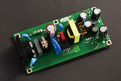
PCB Assembly,PCB Manufacturing,PCB design - OURPCB
Carrying large currents on the PCB requires some design modifications and rules. everything that's needed to be known when designing a high current PCB.
cinder anchor
olive sequoia
I'm new to PCB design and have been playing with KiCad for a project. My concern...
do you have something on that board that draws 30 A?! 👀
olive sequoia
cinder anchor
do you have something on that board that draws 30 A?! 👀
The boost converter is for a dc pump that will pull between 14-20A at 18VDC I have a 12VDC battery/charging system so when doing the synchronous booster design my max current at my lowest voltage is actually just shy of 32A. Worth noting the pump will not run all the time at 18VDC and the booster controller has a bypass mode where I can run the pump at the input voltage.
cinder anchor
olive sequoia
The boost converter is for a dc pump that will pull between 14-20A at 18VDC I ha...
Got it.
heavy jasper
You can also just do more layers, and double them up.
limpid nest
2 Oz copper many layers stitched together?
heavy jasper
Or even just 1 oz
Remember that e.g. desktop motherboards are feeding hundreds of amps into chips and they mostly do it with only a few layers and careful short routing.
I’d be more worried about the design of the 360W boost converter.
That’s a not-insubstantial piece of design, even though the boost ratio is relatively low.
Whatever thermal solution is needed for cooling the power switches in that design will probably be just fine for cooling the relatively small heat output of the PCB traces.
verbal moss
supple pollen
In most cases, it means the manufacturer cheaped out on the capacitors, so they ...
Cheers for this info. Haven't powered up my first jlcpcb design and am already regretting using electrolytic cap 105deg 2000hr 470uF (LCSC # C87858), will look for polymer with better specs for next revision. Mostly powering ~24 neopixels, night light. Outdoor encased project, conformal coating everything, hoping for the best.
supple pollen
verbal moss
Cheers for this info. Haven't powered up my first jlcpcb design and am already ...
That's still better than cheapie 85°C capacitors, and I suspect your project isn't very hard on capacitors, and is undemanding (if the capacitor becomes only 300µF after a couple of years, it should still work), so you should get a few years out of it.
supple pollen
olive sequoia
I'm new to PCB design and have been playing with KiCad for a project. My concern...
One trick is to omit soldermask on the high current traces and beef them up with solder or even more so by soldering some heavy wire along them.
olive sequoia
heavy jasper
Remember that e.g. desktop motherboards are feeding hundreds of amps into chips ...
I hadn't thought of doing multiple layers. Honestly more than two layers seems like such a big jump. I am using a synchronous boost controller with some large MOSFETs to get an estimated 97% efficiency but yeah four watts isn't a little amount of heat to handle for the high side fets.
limpid nest
olive sequoia
I hadn't thought of doing multiple layers. Honestly more than two layers seems l...
Going from 2-4 layers was easier IME
heavy jasper
If you'd be willing to share the schematics, I could take a quick look to see if there's anything clearly worrisome.
97% efficiency for that setup is definitely possible, but is not trivial to achieve, and even with that high efficiency you're going to be dissipating 11W of heat, so it's worth thinking a bit about the thermal solution.
spice turtle
I was going to tag Kattni (I dont know if I can or not) and ask her direct about this, but maybe someone here knows:
https://github.com/adafruit/Adafruit-MicroLipo-PCB
Is there a BOM for this? Im specifically looking for the USB connector as it looks easily solderable.
 brisk cradle
spice turtle
I was going to tag Kattni (I dont know if I can or not) and ask her direct about...
brisk cradle
spice turtle
I was going to tag Kattni (I dont know if I can or not) and ask her direct about...
Which connector?
spice turtle
brisk cradle
Which connector?
The USB connector
brisk cradle
spice turtle
The USB connector
Ok, and which one? There is picture with USB mini, micro and USB-C connector 😉
spice turtle
brisk cradle
Ok, and which one? There is picture with USB mini, micro and USB-C connector 😉
Micro.
tough matrix
I can't say for Adafruit one, but I am happy to share my favorite microusb connector
Order today, ships today. 10118194-0001LF – USB - micro B USB 2.0 Receptacle Connector 5 Position Surface Mount, Right Angle; Through Hole from Amphenol ICC (FCI). Pricing and Availability on millions of electronic components from Digi-Key Electronics.
spice turtle
Is it easy to solder? I have a problem with the insides melting
Unless Ive been using too high of a temp when using a air gun
 grand maple
is anyone here available for doing a small pcb design job i dont really understand how to design pcbs and there aren't that much good tutorials for it
heavy jasper
I’d beg to differ about there being good tutorials in the world, but if you’re looking for a contractor, the adafruit jobs board is a good place to post.
unique patio
Find maker jobs in 3D and CAD, Art, Design, Education, Embedded Development, Engineering, Fabrication, Marketing and Communications, and Web Development
grand maple
what would you consider the "easiest" free pcb design software
heavy jasper
I think Kicad is the standard recommendation for folks just starting these days. All tools have some quirks, and TBH once you’ve learned one it’s pretty straightforward to hop from one to another.
As for USB connectors: Everyone, please, I beg you - stop designing in micro-USB. The sooner folks stop using it, the sooner that abomination will go away.
(This is a purely personal opinion - not anyone’s policy)
spice turtle
USB-C just looks harder to solder is all
spice turtle
grand maple
what would you consider the "easiest" free pcb design software
Eagle but only because Ive been using it for a while
heavy jasper
There's this connector: https://www.digikey.com/en/products/detail/gct/USB4085-GF-A/9859662 that's entirely through-hole
Order today, ships today. USB4085-GF-A – USB-C (USB TYPE-C) USB 2.0 Receptacle Connector 24 (16+8 Dummy) Position Through Hole, Right Angle from GCT. Pricing and Availability on millions of electronic components from Digi-Key Electronics.
dense gulch
I did find a simple thru hole USB-C connector for usb 2.0 interface.
heavy jasper
or this one: https://www.digikey.com/en/products/detail/gct/USB4105-GF-A/11198441 that's partially surface-mount, but still only has one row of contacts
dense gulch
Oh yeah I was about to post the GCT one haha
I actually bought some recently


Still waiting on boards but should be easy to solder
spice turtle
also thanks. I'll consider using those 🙂
Size isnt a problem for what Im making anyway. I'll have to do a small order for digi as well.
dense gulch
Gotta love when you don't have size constraints!
Part of my reason for choosing these too is because I don't have a microscope at home and wanted to play it safe with soldering haha
I should probably get one eventually but that's a future problem
spice turtle
So then I take it they are pretty easy to solder?
So far Ive done down to MSOP and some QFN packages with care. but the Micro USB pins are a PITA
dense gulch
Well I haven't soldered them yet 😄 but from the connectors I have in hand it doesn't seem like it will be too difficult with a thin solder tip / thin solder
Hopefully this week I will get some boards though so I will let you know if I have trouble
Pins within the same row have a 0.85mm / ~33.5mil pitch
 molten beacon
The only weird thing is I don't get why those side pins are so small. Like, it's almost impossible to solder them from the bottom
I don't have huge batches, so I solder them from the top, but I wonder how they envision that in mass production.
Maybe there the wavesolder machine has enough thermal mass and flow to let the solder reach up through the pcb
heavy jasper
And pin-in-paste
Though I honestly am not sure why this connector exists for mass-production - if you have a proper stencil/reflow setup you may as well just use the SMT one.
It's great for smaller manual runs though.
molten beacon
Yeah that could also be the case, would have to look if the datasheet says something about that. The default kicad footprint didn't have stencil keepouts, but that could just be an error. Or made for a different type of USB-c connector with longer pins
heavy jasper
Or the person who made the default kicad footprint just wasn't designing for pin-in-paste.
e.g. maybe they were targeting selective soldering
dense gulch
heavy jasper
Or the person who made the default kicad footprint just wasn't designing for pin...
This is cool! I've only known of wave soldering for mass production, but apparently this PiP process has been around for awhile now.
heavy jasper
Yeah, it's pretty sweet
It can be a tad finicky to get the tuning right - occasionally I've had to do builds of just boards of connectors to tweak the stencil until the solder joints look good.
esp. across varying board thicknesses.
dense gulch
Ah I see, did you have any "solder preforms" to call out / tweak as well?
heavy jasper
I've only had to do a solder preform once, for a bigger LGA module with voiding issues.
and there, to be honest - it was mostly the SMT/quality engineers I work with driving the work, so I'm not the best one to speak about the exact decision-making process that led to it.
dense gulch
Well it's good to know that many of the thru hole parts you have used did not need that 😄
heavy jasper
I will also generally spec for both - pin-in-paste is more commonly used for mixed SMT/through-hole parts (like these type-C connectors)
Whereas bigger through-hole connectors (think bulkheads, DB9s, etc) were done with selective soldering - the big rule there being to keep a comparatively huge (4mm) clearance from the edge of the pads to any surface-mount components. Annoying when you want to put filter capacitors right at the connector.
brisk cradle
grand maple
is anyone here available for doing a small pcb design job i dont really understa...
What you wan to make? PM me 😉
spice turtle
This is an odd issue. I imported the eagle lib for the USB4085-GF-A connector. In the library, its fine. But once I add it to my board, the pins go out of wack
Screen shots below

This is from the library
This is from the board I added it to

What could be causing the pins to become bigger?
Ive never seen eagle do this before
heavy jasper
My guess is that there’s some interaction with minimum annular ring DRC rules
spice turtle
heavy jasper
My guess is that there’s some interaction with minimum annular ring DRC rules
that did it. I put the min's at 6mils and it made them smaller
 glacial gale
does a company like ARM license out their PCB designs? I want to know exactly what they are selling to their customers
unreal flax
glacial gale
does a company like ARM license out their PCB designs? I want to know exactly wh...
Mostly it would be the silicon chip IP cores that are licensed, though they probably also have some reference PCBs that customers could access.
glacial gale
unreal flax
Mostly it would be the silicon chip IP cores that are licensed, though they prob...
https://whatis.techtarget.com/definition/IP-core-intellectual-property-core oh like this right. Would it be soft cores they're licensing out, since its more flexible and changeable on the fly

WhatIs.com
An IP (intellectual property) core is a block of logic or data that is used in making a field programmable gate array (FPGA) or application-specific integrated circuit (ASIC) for a product.
unreal flax
glacial gale
https://whatis.techtarget.com/definition/IP-core-intellectual-property-core oh l...
I expect they would probably also have some designs optimized for specific silicon processes in addition to more generic soft cores, but that's just an assumption on my part.
heavy jasper
https://www.anandtech.com/show/7112/the-arm-diaries-part-1-how-arms-business-model-works is an old but still relevant read.
 limpid nest
I have a 2-row multi-position connector. One one column of that connector, one of the two pins is floating and one is grounded. What are some good ways to concisely show that in a silkscreen? Let me draw a pic real quick


a vertical GND | NC is what I came up with first
It's surprisingly hard to do a sideways N
unreal flax
limpid nest
It's surprisingly hard to do a sideways `N`
Erm, at the risk of stating the obvious, you can rotate text elements 90 degrees.
limpid nest
Oh I meant on a white board lol
unreal flax
Gotcha, LOL 😂
limpid nest
Well i can't make any changes because I froze my PC trying to edit a solid model!
Yup completely frozen!
heavy jasper
If you have space on the board, I’d just label each pin individually, in two columns of text.
limpid nest
Two columns when viewed horizontally? That's what I'm currently doing, or something similar. My other pins have an easy to decide naming scheme.
heavy jasper
I guess it would be two rows as you’ve drawn it above - and the text next to each pin, not the bar between to demarcate.

The way you have it drawn above can be a bit confusing: is the NC the label for the pin that's immediately adjacent, or are the two labels in order, just offset? (I'm pretty sure you mean the latter, but it's easier to misinterpret)
limpid nest
Ahh yeah
The connector is board edge so I don't have the option of doing one label on each side
I guess I could move it in, I'll need to check the connector specs again
 cedar shuttle
hi, I'm trying to make a PCB for an Arduino phone, for charging the lipo battery I'm using the Adafruit Micro-Lipo Charger with USB Type C port schematic if want to use the same port for charging and programming do I need to change the pullups to pulldowns?
 supple pollen
cedar shuttle
hi, I'm trying to make a PCB for an Arduino phone, for charging the lipo battery...
supple pollen
cedar shuttle
hi, I'm trying to make a PCB for an Arduino phone, for charging the lipo battery...
The answer depends on what you're actually doing. Do you have a LiPo in the phone and an external charger, or are you including a copy of the charging circuitry in the phone and powering it from the phone's USB-C port and an external USB power supply, or what?
cedar shuttle
I'm trying to have the esp32 being programmed using the d+ and d- pins
cedar shuttle
full charging schematic
worldly schooner
cedar shuttle
I'm trying to have the esp32 being programmed using the d+ and d- pins
Which ESP32? I don't believe the programmer should ever need to renegotiate as a Host unless you have plans to integrate OTG. https://cdn.sparkfun.com/assets/b/5/1/0/9/SparkFun_ESP32_Thing_Plus_C.pdf is the schematic for SparkFun's ESP32 thing plus. For ESP32-S2, https://cdn-shop.adafruit.com/product-files/5029/5029_TinyS2_P1_Schematic.pdf is the schematic for UnexpetedMaker's TinyS2. Both are commercially available open-source ESP32 boards with USB-C ports and Lipo chargers, for your comparison.
cedar shuttle
esp32 Core Board V2 (DevKitC) http://dl.espressif.com/dl/schematics/ESP32-Core-Board-V2_sch.pdf
worldly schooner
cedar shuttle
esp32 Core Board V2 (DevKitC) http://dl.espressif.com/dl/schematics/ESP32-Core-B...
That board doesn't break out the USB port. How do you plan to connect the USB port to your PCB?
cedar shuttle
this is the USB-c port I plan on using https://lcsc.com/product-detail/USB-Connectors_Korean-Hroparts-Elec-TYPE-C-31-M-09_C2689967.html
Korean Hroparts Elec Korean Hroparts Elec TYPE-C-31-M-09 US$0.4851
LCSC electronic components online Connectors USB Connectors
- leaded datasheet+inventory and pricing
I want to use the USB port for charging and programming
this is the USB part of the board
 worldly schooner
Yes, but are you wiring the pins to your pcb with jumper wires?
cedar shuttle
I plan to build the esp32 on the PCB to make it as slim as possible
worldly schooner
cedar shuttle
I plan to build the esp32 on the PCB to make it as slim as possible
If you're doing a custom PCB design, have you considered using an ESP32 module instead of the devkit? https://www.adafruit.com/product/3320

The ESP8266 started a small revolution by bringing WiFi to a small and cheap package that also had enough processing power and enough pins to get small things done. Now get ready to take ...
cedar shuttle
ok thanks
steel valve
Putting a LDO Regulator into my PCB, how do I pick a good one? I want the output to be 1.8V, I am doing this for a LiPo battery http://cdn.sparkfun.com/datasheets/Prototyping/spe-00-DTP401525-110mah-en-1.0ver.pdf
So far the only one I think that would work is this one, but seeing if there are any cheaper ones and also if this one would truly do what I want it to
https://www.digikey.com/en/products/detail/analog-devices-inc/ADP150AUJZ-1-8-R7/2207484
Order today, ships today. ADP150AUJZ-1.8-R7 – Linear Voltage Regulator IC Positive Fixed 1 Output 150mA TSOT-23-5 from Analog Devices Inc.. Pricing and Availability on millions of electronic components from Digi-Key Electronics.
unreal flax
There should be lots of other options on Digi-Key. Here's the cheapest comparable one from a manufacturer I recognize: https://www.digikey.com/en/products/detail/microchip-technology/MIC5365-1-8YC5-TR/1868082
steel valve
unreal flax
There should be lots of other options on Digi-Key. Here's the cheapest comparabl...
Ohh ok i was looking on mouser originally which is how i found that other one (it was oos on mouser but checked digikey and they had it)
tough matrix
mouser also has a lot of options: https://mou.sr/3p6icKU
spice turtle
steel valve
Putting a LDO Regulator into my PCB, how do I pick a good one? I want the output...
For battery powered stuff, pay attention to quiescent current. The lower it is, the more $$ as well.
steel valve
unreal flax
There should be lots of other options on Digi-Key. Here's the cheapest comparabl...
Do you happen to know a slide switch that isn't like 10mm long cause I keep finding really big ones on mouser and digikey and can't seem to find any that are tiny

(For perspective the footprint is 10mm long on a 5mm pcb, and yes I know the parts are too close to each other I will be fixing that once I find a proper switch unless this happens to be just how small slide switches can get)
supple pollen
Pretty small? These are 6.8mm long

C&K PCM series are smaller (by all of 100µm)

Slightly larger at 7.65mm, but it's illuminated!

 viscid coral
Has anyone done via in pads in EAGLE before? (I think they are also called vippo --- via-in-pad plated over). I followed the instructions here: https://forums.autodesk.com/t5/eagle-forum/microvias-won-t-place-eagle-9-3/td-p/8556848.
Though the via in pad still brings up a clearance error on the DRC and a blind via ratio error. Although I made the blind via ratio 0.1 like in the above instructions. I examined one of SparkFun's boards with a similar component (MAX32664, while I'm using the MAX30001) and it seems that they just approved the error. Is that the process here (at least in EAGLE)? I'm working with a 30-ball BGA with 0.5 mm pitch. Board will be at least 4 layers with a signal, ground, power, signal stack-up. traces/clearance will be 4/4 mil.


 steel valve
supple pollen
Pretty small? These are 6.8mm long
steel valve
supple pollen
Pretty small? These are 6.8mm long
I am saying the footprint in its entirety (+ pads)
But anyways I'll just use this since I don't think there's anything smaller
limpid nest
viscid coral
Has anyone done via in pads in EAGLE before? (I think they are also called vippo...
Not sure that this is your issue, but the issue I had was that all the vias on a particular pad needed traces between them for some odd reason
viscid coral
limpid nest
Not sure that this is your issue, but the issue I had was that all the vias on a...
That fixed your clearance error? Did you get a Blind Via Ratio error as well?
limpid nest
Ah I misread, hmmmm not 100% sure! I think I just approved my clearance errors
viscid coral
limpid nest
Ah I misread, hmmmm not 100% sure! I think I just approved my clearance errors
Okay. One more question if you don't mind. Should the outer annular ring extend wider than the BGA pad?
steel valve
It's kind of annoying having to manually figure out what's the center along a certain axis
limpid nest
viscid coral
Okay. One more question if you don't mind. Should the outer annular ring extend ...
That I don't know, I don't know much about BGA design
viscid coral
limpid nest
That I don't know, I don't know much about BGA design
No problem. Thanks for chiming in.
limpid nest
np
limpid nest
If I want to buck 12V to 5V, I want a positive output configuration, correct?
supple pollen
Normally. I'll often just use a UBEC for that.
limpid nest
interesting
I'll look into that. I was looking into linear regulators but I may need multiple amps and that's a lot of power to burn
The attraction of linears is they have very few external components
supple pollen
For up to 3 amps, I just use the UBEC that AdaFruit sells. For more current, Pololu has a variety of nice offerings.
limpid nest
I'll have to crib from adafruit but I'm not above that!
supple pollen
I just use the UBEC as if it were a component.
limpid nest
Ah I think I need more than 3A
supple pollen
Pololu offers 4, 5, 9, and 15A versions
limpid nest
I guess I could make a footprint for one of those and just solder it on
supple pollen
That's how I like to do it.
limpid nest
Although pin headers supposedly can't take more than 3A
supple pollen
For high current, you could double them up, use terminal blocks, or solder (heavy) wires directly to the board
limpid nest
digikey has some high current headers