#help-with-hw-design
1 messages · Page 59 of 1
 twilit mango
 distant raven
Any TI LDO
What voltage do you want?
If you need 3.3V the TLV75533 is decent
Texas Instruments Texas Instruments TLV75533PDBVR US$0.5086
LCSC electronic components online Power Management ICs Linear Voltage Regulators (LDO)
- leaded datasheet+inventory and pricing
LCSC is the only place I’ve ever found them
All other places are 2023 lead times
 limpid nest
I've had someone buy all stock on digikey for a part 3 times in the last week. Stuff is cray
distant raven
Yikes
limpid nest
I'm playing with smaller vias in Fusion360, going from 0.35mm to 0.2mm specifically. Here's what a normal sized via looks like

When I size down to 0.2mm, I get this. Anyone know what's up?

 unreal flax
limpid nest
When I size down to 0.2mm, I get this. Anyone know what's up?
unreal flax
limpid nest
When I size down to 0.2mm, I get this. Anyone know what's up?
You may want to clarify what you mean by "what's up".
limpid nest
They look "fine" in manufacturing preview
limpid nest
unreal flax
You may want to clarify what you mean by "what's up".
Good pt lol
There isn't a visible "hole" there, and there's that green cross hatch section.
unreal flax
The hole is probably smaller than the red trace now. I'd suspect that the green circle is marking a DRC error because the via is smaller than the minimum drill size you have configured.
limpid nest
ahhh ok, let me look at my minimum
in DRC
Changing DRC minimum drill fixed it. I can now see the hole too with the green cross hatching gone. Is it a bad idea to use .2mm holes? JLCPCB claims they can do it.
unreal flax
If they're happy with it, there shouldn't be a problem. Just be sure to follow the related guidelines like the annular ring sizes... you want that surrounding pad to be big enough to handle any imprecision in where the drill hole will actually go.
limpid nest
I left the annular ring DRC settings unchanged. Should I change them?
unreal flax
It's generally a good idea to do a scrub of all of the settings versus JLCPCB's requirements. The Fusion defaults are just guesses, not a guaranteed "good" config.
limpid nest
ahh ok thx
It looks like the default/auto is within JLCs requirements. I could go smaller if I wanted to

My kingdom for a prototyping house that will do blind and buried vias.
thanks for the pointers @unreal flax
unreal flax
Lots of places will do that, it just is extra 💸, heh heh.
limpid nest
ah ok good to know, I thought that most proto houses don't do it periods.
 supple pollen
It's rarely required unless you're using BGA chips or other high-density techniques.
limpid nest
Sometimes I just want to use fancy tools
 quartz shadow
Quick question about parts. I'm not sure what to call it to look for it, but when you have a screw (or nut I guess really) soldered down to your pcb, like for an m.2 ssd.
What do you call that screw bit?
supple pollen
AdaFruit seems to call them "standoff nuts": https://www.adafruit.com/product/4207

These brilliant solder-able standoffs will make your mechanical PCB mounting problems go away. They're super simple - round M3 standoffs that are coated with tin so you can solder them ...
quartz shadow
Yes! Thank you!
limpid nest
Anyone have an idea what layer this is in this part? I can't select it to Rclick > Properties.

the slashed portion
Overall I'm trying to figure out why F360 won't let me put a via on the THERM part
unreal flax
The white-slashed layer is probably the soldermask. Normally you wouldn't edit that independently of the pads, but it's probably not interfering with the via placement.
limpid nest
I'm not used to seeing the soldermask on the part. Let me go thru and turn off every layer that's on until I get an answer
unreal flax
Likely tStop.
limpid nest
unreal flax
The white-slashed layer is probably the soldermask. Normally you wouldn't edit t...
It's tStop. Isn't that the opposite of soldermask?
Like that says "don't put soldermask here", I thought
unreal flax
Yes, that's correct.
limpid nest
ok cool. Would that prevent a via? The I can place it fine, but the via actually populates here (blue squiggle area)
 unreal flax
No, it shouldn't. Maybe vRestrict isn't being shown?
limpid nest
also wonder why there's not just a large patch of tCream, but instead 6 squares
vRestrict is being shown and isn't present, it seems
unreal flax
The squares is to give the solder paste a little room to be squished down by the chip.
limpid nest
ahhh
ok
Ok it took fusion360 crashing to work, but now I can place vias no issue
So weird
 cinder anchor
limpid nest
Ok it took fusion360 crashing to work, but now I can place vias no issue
cinder anchor
limpid nest
Ok it took fusion360 crashing to work, but now I can place vias no issue
they probably pushed an update in the middle of you doing that... 😄
limpid nest
Lol
limpid nest
If I have a P channel MOSFET that's dealing with relatively high current (say 3 Amps at 5V) do I need a polygon for a pin that's connected to ground? Or can I just use a trace?
unreal flax
A trace-width calculator suggests 1.4mm for 3A current and a 10-degree temperature rise, for example.
limpid nest
hmmm ok, one sec let me get the circuit. The gate is grounded in this case, so current is flowing drain to source. I'm going to use polygons for those
unreal flax
So you're just asking about the gate? That should have negligible current, so you don't need anything special there.
 unreal flax
With the caveat that I am really bad with transistors, I think you might have the drain and source backwards there, since the body diode is pointed in the wrong direction.
 tough matrix
it would be correct if the MOSFET is used not for switching the current on/off but for reverse polarity protection
limpid nest
tough matrix
it would be correct if the MOSFET is used not for switching the current on/off ...
This is correct
That's a screenshot from a video about reverse polarity protection
In this configuration the fet is always "on" and conducting current
 heavy jasper
Gates are high-resistance at DC; a thin trace there is fine. Make sure you’re not exceeding the Vgs(max) of the FET in this configuration - you’ll often see a resistor/zener combo there to clamp the gate voltage in a safe region.
 ember laurel
@limpid nest I think it would make sense to put something like a 10k resistor between Gate and GND here
and a Zener from Gate to Src.
 worldly schooner
quartz shadow
What do you call that screw bit?
worldly schooner
quartz shadow
What do you call that screw bit?
We call em PEMs in my office, but really that's just the one manufacturer that makes all of the ones we use. SMTSO is our default surface-mount threaded standoffs, but there's a pretty good variety here: https://www.mouser.com/datasheet/2/974/kdata-1901229.pdf
quartz shadow
worldly schooner
We call em PEMs in my office, but really that's just the one manufacturer that m...
Thank you!
unreal flax
For Eagle / Fusion360 users, it looks like Autodesk has a 30%-off sale on subscriptions going on now. (They often have a New Year deal like this.)
tough matrix
@quartz shadow if Adafruti and Mouser do not carry the size you want, you can also get them on AliExpress - just search for SMTSO
quartz shadow
tough matrix
<@!419340812820807680> if Adafruti and Mouser do not carry the size you want, yo...
The size I need is M2.5 for mounting a pi zero to a custom PCB
I found the product detail sheet for them, and know how to put together the model number I need. Thank you all.
 golden spade
Hi! Is there a way to use a WLP package with a 0.4mm pitch on a custom pcb with a reasonable price? I prefer jlcpcb but I don't think they can manufacture it
worldly schooner
golden spade
Hi! Is there a way to use a WLP package with a 0.4mm pitch on a custom pcb with ...
JLCPCB can probably just manage smaller WLP packages on their 4-layer boards; I don't know of an easy way to do it on a 2-layer board without paying some good money for tighter dimensional clearances...
golden spade
the ic has 54 pins and will definitely need via's between the pins but jlc's minimum via diameter is 0.4mm so it wont work
distant raven
golden spade
the ic has 54 pins and will definitely need via's between the pins but jlc's min...
I’ve done 0.254mm without issue through JLC
And I’m certain the minimum size for 2 layer is 0.2mm
golden spade
distant raven
And I’m certain the minimum size for 2 layer is 0.2mm
that is the minimum hole size but minimum diameter is 0.4mm on multiple layer boards
distant raven
These use 10mil (0.254mm) via

From JLC
You’re looking at total size, I see
Yeah 0.4mm
But via drill is 0.2mm
Your biggest issue is going to be minimum BGA spacing
0.127mm between pads
golden spade
yeah true, so the total size would have to be around 0.2mm
distant raven
You could do. 0.45mm pad with 0.4mm via in pad
That’s a valid option so long as you don’t pay for fill and plating of the via
distant raven
Or even 0.42mm pads to have a little extra tolerance
golden spade
this is the package
golden spade
yeah true
distant raven
Unless you can find a place to cheaply do 4/4 or 3/3 with 4-5mil via drill
Which is laser drilled and expensive
3/3 meaning trace width and spacing
golden spade
I am not aware of any service that could do it but I dont know them all
distant raven
You can do really advanced stuff through PCBWay but it’s expensive
Talking a few hundred $$
golden spade
yes true, but would be too expensive 😦
 golden spade
BGA's are really hard
distant raven
It’s true
worldly schooner
BGA's ain't cheap to work with, after all. That's why the TQFP packages all go out of stock first...
golden spade
yeah, I guess I will have to find an alternative
limpid nest
heavy jasper
Gates are high-resistance at DC; a thin trace there is fine. Make sure you’re no...
V gs max is 20 V so I left the zener and resistor off
ember laurel
@limpid nest ESD?
limpid nest
ember laurel
<@!887510739462537236> ESD?
I added a TVS diode between Source and GND
limpid nest
Can this transistor https://www.digikey.com/en/products/detail/nexperia-usa-inc/BSS138BKW-115/2779824 be used as a drop in replacement for this one https://www.digikey.com/en/products/detail/onsemi/BSS138/244210 for the purposes of driving an LED?
Unrelated, can't figure out why I'm getting an airwire here. Hard to see so I've circled it. The name of the via is GND and it goes to my GND plane.
 unreal flax
Just draw a trace on top of the pad... Eagle/Fusion is sometimes a little fussy about seeing via-in-pad scenarios as connected.
limpid nest
ahhh ok thanks
limpid nest
is there a way to restore the silkscreen name of a part? I accidentally deleted the name IC2 for one of my ICs but it must have been a while ago so I can't CTRL+Z it.
fusion 360
limpid nest
limpid nest
is there a way to restore the silkscreen name of a part? I accidentally deleted ...
reposition attributes
 thick willow
Whats the point or making the pins like that? Is it so that on a round hole the component does not make contact to the pcb?
 limpid nest
that would be my guess
Maybe the solder makes a more mechanically sound connection this way too
Not 100% though
thick willow
On dip they do something similar...
limpid nest
My best guess is it makes a better joint
supple pollen
It's a standoff to lift the part slightly off the board.
thick willow
What would be the point of doing that?
I would think here it would be easier for liquids to get int and maybe short
supple pollen
Several possible reasons. One is to allow board washing to clean up flux. Another is for parts that are easily heat damaged to move them away from the heat of soldering. Another is airflow/cooling.
One engineer told me that liquids always will get in, the idea is to give them a way to get back out.
limpid nest
interesting. I assumed it was so there was more material for the solder to adhere to, thus creating a stronger joint.
thick willow
you could still make it bigger so that everythign fits in the hole
but since they point in opposite ways i figured it was so that it would keep the component rised, just wasnt sure why that would be desireable here
worldly schooner
It's more common for parts with a plastic body that would be more prone to heat damage from solder. If you wanted a surface mount, you could potentially trim and file the pins and use the remaining surface to connect it that way, in exchange for mechanical durability.
thick willow
I'll just make the hole bigger. I use low temperature solder anyway
ember laurel
distant raven
These use 10mil (0.254mm) via
Is that JLC's PCBA as well?
 limpid nest
I have one of these (https://www.tripplite.com/4k-hdmi-coupler-with-ethernet-female-to-female-industrial-high-speed-4kx2k-60hz-ip67-rated-dust-cap~p569000ffind) and am confused a bit by the panel cutouts shown in the installation guide. They have one detent but the part itself has 2 detents. Can anyone shed any light?
supple pollen
limpid nest
I have one of these (<https://www.tripplite.com/4k-hdmi-coupler-with-ethernet-fe...
There are basically two reasons: many panel cuts have two, and a one-flat (D shaped) device wouldn't fit. The other is you can just flip it over and mount it in either of two orientations.
limpid nest
reason 2 makes sense, I hadn't seen many panel cutouts with two, in fact the ones they sell for this product are single flatted. Interesting, thanks
ember laurel
@distant raven PCBA with JLC is really cheap
tough matrix
if only they had more parts in their list.
BTW, believe it or not, but right now they have some number of ATSAMD21G18 available for assembly.
distant raven
ember laurel
<@!728676724522352733> PCBA with JLC is really cheap
What’s cheaper than free labor? Lol
worldly schooner
Is it really free when you invest your own time? How much is your time worth?
It's not free, but I guess it COULD be cheaper than JLCPCB...
distant raven
I mean, I’m in it for the enjoyment
Lol
I like building stuff
Well, I’m technically not in it anymore
I closed my business because it was just too much trying to keep up with the business legalities and work
ember laurel
ouch that is hard
what kind of legalities?
@distant raven did someone come knocking on your door?
distant raven
Just tax filing deadlines and whatnot
It’s just a lot to try to track on top of working full time and dealing with some of the things I’ve been dealing with
 flat vigil
ya, taxes on assembled goods it tricky
ember laurel
why?
flat vigil
because you need to account for the cost of each unit to determine your profit from sales
distant raven
Well, that and having to track use tax if you didn’t pay taxes on a part and then sales tax for the sale of a good
The single member LLC bit being an owner means I don’t necessarily have to pay myself a salary since I’m entitled to all profits. But trying to keep track of tax filings both federal and local is exhausting
flat vigil
my local taxes are relatively easy here in washington
ember laurel
hmm I see
cinder anchor
I just got severely triggered by the mention of the T word.
ember laurel
I just hand my bills and invoices over to an accountant that handles it all for me
flat vigil
no goods or inventory
ember laurel
I don't use any ERP or anything though
flat vigil
do you have goods?
ember laurel
I've sold some stuff earlier, but now I'm just about to start up production of a bit larger scale
and yes, goods
most of the stuff comes in from china, and gets assembled here in Liechtenstein
tough matrix
So far I am flying below the radar. No taxes filed.
(Yes, strictly speaking it is illegal. But then, my profits so far are negative: all my revenue, plus quite a bit of my own money, goes into buying new tools and components, so morally I have no issue with it.)
ember laurel
assembly meaning putting boxes and pcbs together, uploading firmware and doing QA etc
tough matrix
of course, I have a very small operation\
ember laurel
I'm looking at some pretty small numbers for 2022 as well
cinder anchor
Ah, he's in Europe. 🙂 So does not have to deal with IRS.
ember laurel
Europe, outside of EU
cinder anchor
Taxes in Europe are still way simpler than in the US.
tough matrix
I am sure you have your own authorities...
cinder anchor
Especially sales tax.
flat vigil
I've had a good experience interacting with the US IRS. I do my own taxes and they've corrected me a couple times
ember laurel
I'm planning to sell units for $100k something this year
of which $35k would be costs
flat vigil
nice!
cinder anchor
I am currently having a really bad experience with the US IRS. They "lost" 5 years of paper returns, and says I owe them money. It's most likely the other way around, but, they're going to dig a deep freakin' hole to try to make it not so.
ember laurel
if things go well, I should do $300k in 2023
cinder anchor
Nice!
tough matrix
ember laurel
if things go well, I should do $300k in 2023
wow. Are you a one-person operation or you use help?
flat vigil
ah, I've been filing digitally through their "free file" site. I've never actually sent some in
we'll see what they do this year since the free file alliance is no more
ember laurel
I have a factory in China handling the PCB+PCBA
here in .li I have outsourced the assembly.
to a buddy's company, he has some spare capacity with his workers.
I'm just doing the QA process, validation software etc
and of course, firmware and app programming etc.
and all the freaking regulatory docs
tough matrix
@flat vigil I do my personal taxes through one of online tax prep companies. Federal is free, state cost me $20
cinder anchor
flat vigil
we'll see what they do this year since the free file alliance is no more
it's bad... we still haven't gotten our taxes straightened out from 2020-2021... I guess they sent so much money out to random people that they're trying everything they can to recoup some of those losses 😄
cinder anchor
like, we are still... just waiting around...
yeah, I don't think the others picked up on that
flat vigil
hopefully the new funding will let them focus on the richer folks
cinder anchor
Lichtenstein. That's what's up.
flat vigil
@tough matrix that's good! They were supposed to let 70% of americans do that
tough matrix
flat vigil
ideally we'll get to return free filing sometime soon
ember laurel
the one thing I'm wondering about, would be the Trump tax in the US
I think I would be free of that, since I can claim made-in-liechtenstein
(even though all components come from china)
worldly schooner
Lmao only in the USA do we have to pay to file our taxes. Murica.
tough matrix
you mean tariffs on china goods?
ember laurel
yeah, the Trump tariff
20% flat on pretty much everything
(with a 2 bajillion page book for exemptions)
tough matrix
yes... for one small project I did, the order was under $800, so they let it go tariffs-free. Not sure how real electronics manufacturers like adafruit deal with it
ember laurel
I think I can claim made-in-liechtenstein, since assembly, QA and software are all made here
and over 50% of added value
tough matrix
but custom duties on components?
ember laurel
I don't think that would be applicable
worldly schooner
No, you definitely can. They wouldn't put tariffs on manufactured goods with raw materials sourced from China. That would literally become a flat tariff on almost every good that comes into the US...
ember laurel
it is just a "medical device" really.
flat vigil
hopefully we'll get return free filing soon. it won't help with small businesses doing assembly though
flat vigil
tax policy is one way general policies are implemented
cinder anchor
I'm from Sweden and I think for me the most jarring experience has been taxes by far.
ember laurel
are swedish taxes complicated?
cinder anchor
No, they are simple. Just a tad high. But, when it all comes down to it, I pay just as much taxes here in the US (percentage-wise), so I dunno.
ember laurel
they're just really high, but I'm not sure about complicated 🙂
I'm also a swede, you know 🙂
cinder anchor
Oh, yeah? 😄 Nice!
ember laurel
one of the reasons I moved was the taxes
running your own company with the swedish taxes just wasn't so cool
cinder anchor
tell me about it...
ember laurel
considering I'm in software in my day job, I can live pretty much where I want
cinder anchor
I sort of can, but, I can't move to certain parts of Europe and keep my salary, unfortunately. So, no cheap tax havens for me.
tough matrix
my son is planning his career now (he is in software too), and says he and his girlfriend plan to travel the world while workign remotely for California company
ember laurel
that's something I find pretty difficult though
I tried that for 6 months
was hard to focus
and time zones make a mess of communications
I'm working a lot with a Cali company right now, and the 9h time difference is just really hard to deal with, if people are on regular office hours
tough matrix
yeah
Let them find it out
Out of question for me though
ember laurel
all in all a nice experience - so if he has the opportunity, he should go for it 🙂
cinder anchor
yup, the "tech nomad" life appeals to some... they just need to get off Instagram and try it in real life, it's definitely not as glamorous as they think... but, they'll learn a lot and have a good time still...
ember laurel
for electronics it is difficult... you need somewhat of a lab
cinder anchor
Get an RV with a trailer. Build benches in trailer.
Friend of mine is a nomad blacksmith. Just finally settled down with a "real" job as an educator.
ember laurel
and.... drive it through China?
cinder anchor
Yup. Drive it straight through China.
flat vigil
I worked for adafruit from barcelona for 4 weeks early on when I started
cinder anchor
Just don't try to visit like Nepal or Tibet or something, because those mountain roads are killer. 😄
ember laurel
not sure the Chinese would like the US plates
one of the best things about Liechtenstein would be our number plates
they're badass black
 ember laurel
1 of course belongs to the almighty ruling prince
ember laurel
one of the few absolute monarchies
cinder anchor
I kind of miss hearing about Knugen and Silvia.
ember laurel
prince has the power to veto anything voted for by parliament.
cinder anchor
(Background for those that are not in on the joke: Kungen means "The King" in Swedish, and our benevolent King Carl XVI Gustaf happens to be dyslexic. He signed some royal proclamation "Knugen")
it was basically everything anybody talked about for weeks
and Sweden also has a pretty awesome history of people sneaking into the castle and throwing cream pies at the king
worldly schooner
Can't say I'd recommend going to China right this moment, but definitely worth taking a mobile electronics lab to if possible haha
Oh I didn't scroll down all the way...
cinder anchor
So, why shouldn't one go to China right now? Omicron?
ember laurel
do they let anyone in?
worldly schooner
Yeah. Chinese pandemic countermeasures are a tad on the overkill side rn.
If you go, you'll likely get stuck for a while...
worldly schooner
ember laurel
do they let anyone in?
I think so, as long as you have time to sit through quarantine and a half.
cinder anchor
oh wow
worldly schooner
I hear it's a bit easier too if you're not coming from the US.
A lot of political tensions I'd rather not discuss here.
But I miss Shenzhen.
cinder anchor
I am sure. It's usually easier to travel as a non-US person, anywhere.
I have never been to China. I really want to go see the wall.
worldly schooner
Honestly almost every urban area has a nice electronics market somewhere...
But Shenzhen is something else...
cinder anchor
I also kind of want to go to India, but I am not a fan of crowds, and they have lots of crowds. Like, insanely large, thronging masses of people... being people...
worldly schooner
All the random electronics components for sale I wish I bought more of.
cinder anchor
I saw some videos of PC Jesus in Shenzhen, that was some wild stuff.
worldly schooner
It's too bad my China trips predated most of my actual engineering experience. The things I could do with that today.
cinder anchor
Yeah, I wish I had rediscovered electronics sooner.
I took an extra-curricular in grade school called "Hem & Teknik." I obviously didn't care much about the Home part, and was only there for the Tech. But, I've done wild things, like etch my own circuit boards the old fashioned way.
Bet you they won't let the kids do that these days. 😄 Seen a few kids hit the eye shower in my day. 😄
 woven pagoda
what's a good drill press for pcb? Looking to buy something soon.
 proper anvil
I've received the assembled prototype for this board I designed, which uses a 555 timer and a mosfet to control motor speed, and a three-way switch to control forward/off/reverse. It worked great initially, but after testing for a while, I've lost speed control. It stays at full speed all the time, which to me, sounds like the mosfet died closed. The mosfet is far overspecced for the motors we're using (to keep it cool without a heatsink) so the only thing I could think of is that I configured the flyback diode wrong. If someone's got a spare minute and could check my schematic I'd greatly appreciate it. Included a screenshot, and also a PDF if you want to zoom in.

 heavy jasper
Have you confirmed that the MOSFET is actually failed short with a multimeter? It’s a reasonable theory, but also good to confirm before tunnel-visioning on how to fix it.
heavy jasper
I’d have to math out what your expected drive frequency is, but worth noting because the FET is so thermally robust, it also has a pretty large gate charge (especially at 9V drive) - it’s essentially like a 10nF capacitor. Based on the risetimes of the ne555, it looks like you’re probably in output current limiting every time you drive the gate, if the 555 actually limits (it may not - in which case you may just be burning out the high-side switch on the output drive stage of the 555). If your MOSFET seems fine when you measure it, that’d be the next thing I’d look at (a short from VCC to OUT).
 elder peak
I have to say it was fun being in Prague and seeing the windows where the Defenestrations Of Prague happened.
proper anvil
heavy jasper
I’d have to math out what your expected drive frequency is, but worth noting bec...
If the issue Is burning out the 555, would a solution be adding a current limiting resistor on the signal line?
heavy jasper
Yes, that could be a good solution.
proper anvil
heavy jasper
Yes, that could be a good solution.
Okay well thank you so much for your analysis and your time.
 last prairie
I'm trying to build a pcb with the itsybits m4 soldered on it but when I look it up on the internet it gives the actual schematic of the itsybitsy whereas I just want the footprint that will allow me to connect the itsybits onto my board via through holes, where can I find this and what do I have to search for.
cinder anchor
last prairie
I'm trying to build a pcb with the itsybits m4 soldered on it but when I look it...
 heavy jasper
It's not quite fully dimensioned... I'd probably pull either the step file to confirm, or the .brd file and then copy-paste the pads out
Adafruit does release the part in fritzing; not sure if that's useful to you directly or can be converted.
And you can probably guess at the dimensions fairly well - each of the big vias will be 0.1" center-to-center because it's meant to go on a breadboard
and the holes are probably evenly spaced left-to-right, so you can put out the correct number and center them vs. the 1.4" overall L-R board dimension
heavy jasper
If you dig around a bit, someone may have made a kicad or EAGLE element for it in a standard library, I'm not sure.
Or, as mentioned, if you're using fritzing, I think Adafruit does released a rendered/footprinted version there.
cinder anchor

Adafruit Learning System
What's smaller than a Feather but larger than a Trinket? It's an ItsyBitsy!
last prairie
uh
cinder anchor
the M4 has the same footprint as the 32u4
cinder anchor
and there's fritzing and EAGLE files there
yup
the pinout is different, though, so bear that in mind
last prairie
but dis is not what I really want:
most companies give me this

when I want this:
 cinder anchor
So, what are you looking for in this case? What was wrong with the files in the article above?
last prairie
they provided the actual schematic to make the board
I want the schematic to allow me to wire up the board to my pcb
cinder anchor
Alright, so do you have the schematic for your PCB?
last prairie
@cinder anchor how do I just find the simple one (second image) is there like a word I have to use in google
 supple pollen
You can either take the ItsyBitsy design and delete everything but the pads, or just take advantage of the fact that the pins are at a 0.1" spacing and make a footprint for it that way.
Or just use two 1x14 headers, spaced 0.6" apart.
I too like using boards like that as plug-on daughterboards (in this pic, I'm using a Teensy 2 that way)
 supple pollen
Yes, I'm quite happy with them. I use them and ItsyBitsys in a lot of projects
That Teensy footprint is in my Eagle library: https://gitlab.com/bodger/bodger-lbr
 last prairie
thx
last prairie
@supple pollen do you have an itsybitsy library or know of one that I could use for soldering it to my PCB, if not I'll make one but I just wanted to check.
last prairie
@supple pollen
 spice turtle
😅 I wouldnt ping someone more than once 👀
supple pollen
last prairie
<@!348911944486486016> do you have an itsybitsy library or know of one that I co...
I was off having breakfast. No, I don't have one handy, but it's easy enough to just grab the ItsyBitsy design files, delete everything but the pads, and move the outline onto a silkscreen layer.
last prairie
ok sure thx
 iron finch
Hello All, im trying to embed this charger ( Adafruit Micro-Lipo Charger for LiPo/LiIon Batt w/MicroUSB Jack - v1
https://www.adafruit.com/product/1904
) into my PCB. I would like to use the micro USB on the itsybitsy to charge the battery. I was wondering if any one knew if this is the correct way to go about it?
the 1X 10 screw terminal is the Itsy bitsy
https://www.adafruit.com/product/4481
pin 1 is BATT
pin 2 is ground
pin 3 is USB


Oh so handy, this little lipo charger is so small and easy to use you can keep it on your desk or mount it easily into any project! Simply plug it via any MicroUSB cable into a USB port and ...

What's smaller than a Feather but larger than a Trinket? It's an Adafruit ItsyBitsy nRF52840 Express featuring the Nordic nRF52840 Bluetooth LE processor! Teensy & powerful, ...
worldly schooner
iron finch
Hello All, im trying to embed this charger ( Adafruit Micro-Lipo Charger for Li...
The charging part of this schematic looks fine. I compared it to https://www.adafruit.com/product/2124 since that's probably a better reference to what you want it to do, and nothing jumped out to me as a problem.
As for the other parts, I can't speak for the switching speed on the transistors, but the pulldown resistors on the DIP switch side can probably use a higher value for lower current draw in its ON state, as they don't seem to be signals meant to change quickly. (I can't imagine you would use a DIP switch if you did otherwise...)
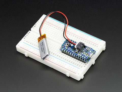
If you have an ItsyBitsy or Pro Trinket you probably know it's the perfect little size for a portable project. This LiPoly backpack makes it really easy to do! Instead of wiring 2 or 3 ...
iron finch
worldly schooner
The charging part of this schematic looks fine. I compared it to https://www.ada...
Thank you Hem for taking the time to look my schematic over. The pull down switches are connected to a 1.5 volt 24 bit data and clock each cycle time is roughly 14 mills. What should I use instead of DiP?
Oh my apologies 😅 the DiP switch is just to turn the power and and off to the micro Controller. I thought you were referring to the transistor on the bottom right
worldly schooner
iron finch
Oh my apologies 😅 the DiP switch is just to turn the power and and off to the ...
I figured that was the case. The pulldown resistors on the DIP switch is continuously draining current through those resistors while power is on, so you can probably use a higher value resistor to waste less power through that resistance. 100k or even 1M shouldn't affect the microcontroller drawing power in any way, and can potentially extend the battery life by a considerable amount.
iron finch
worldly schooner
I figured that was the case. The pulldown resistors on the DIP switch is continu...
Okay I will increase r4 r5 and r1 to 100k or 1m. Should I do the same too r9 and r10?
worldly schooner
I don't know what those signals are, but changing the resistance can affect the rise and fall times of the signal, so it would depend on what those signals are and how they would be affected.
iron finch
Okay ill keep that in mind. Thank you for your assistance.

 worldly schooner
Oooo, more low-profile keebs?
 prime jasper
 silk lark
playing a bit with patterns
silk lark
playing a bit with patterns
Neat. I like the switch via's. At first I was a bit puzzled about the extra hole, but that added symmetry makes it that you can flip it over. So the matrix is in an internal layer?
Oh never mind. I just needed to zoom in. to see the traces.
What are the big holes for? Æsthetics?
limpid nest
when the size of Samtec connector you want fits perfectly in between the immovable mounting holes on your board

now if someone could stop Fusion from crashing all the time, I'd be golden
 pallid ridge
may need some help
im about to learn circuit python so i can write a code for my mega buster
my goal is for it to make the buster sound fx with a press of a button and holding it to activate the charge sequence

heres an example of what im trying to go for
and im a bit stumped on what circuit boards i should use
especially for the mp3 player to play music

Feeling really damn good about this one. Obviously not fully assembled but the program is working well. It was a real pain learning all of the things that went into this so far. The light animations are custom made (I had 0 coding experience before I started this project 1 month ago). I built a mini fogger with a vape atomizer, a 3d designed hou...
Likes
179
 Instagram
 pallid ridge
you did?!!
limpid nest
Let me see if I can remember. I was trying to move away from using the raspberry pi for my work projects since I think it's overkill for what I'm doing.
IIRC, the pi is still the easiest way to play MP3s over an audiojack, even though it's way over kill. Let me see if I can find the CP MP3 stuff I saw
limpid nest
pallid ridge
you did?!!
what level of quality are you looking for? Like do you want it to sound as good as if you played it over computer speakers?
limpid nest
Indeed you can! There are circuitpython libraries that you call when you write regular python on the pi
pallid ridge
awesome
limpid nest
Here's the big guide: https://learn.adafruit.com/circuitpython-essentials/circuitpython-mp3-audio
as well look at this board https://www.adafruit.com/product/3678
There's also a baremetal CP build for the pi but it doesn't currently expose the audio jack
pallid ridge
also the leds. neopixels to have specific animations when reacting to the charge effects
but thats for the coding
dm me these
thank you
limpid nest
Ahh ok hmm
Well
Pi and neopixels don't always mix.
Neopixels need precise timing that the pi struggles with.
In case anyone else is here. I'm wondering about the footprint for capacitors that comes with Fusion360. It has these horizontal (or vertical depending on your PoV) lines on the sides. Should these not overlap when placing caps next to each other?

E.g. is this bad?
 pallid ridge

Adafruit Learning System
Improved prop Sonic Amplifier with CircuitPython and Feather M4
also was looking at the build thread
limpid nest
I suspect you'll be fine with just a CP MCU and don't need a pi
I need really high quality output
You'll want some way to store the music files as they may not fit on the CP board itself.
So an SD card breakout is in order
pallid ridge
okie dokie
Okay making a parts list
Adafruit decoder breakout
Sd cardbreakout
Adafruit prop maker featherwing
Adafruit mono calls d audio amplifier
Adafruit quad featherwing kit
And of course neopixels and large speakers
And the other do dads
limpid nest
pallid ridge
Adafruit decoder breakout
Sd cardbreakout
Adafruit prop maker featherwing
Ad...
This one? https://www.adafruit.com/product/2219
looks like that's only for the pi? Not sure. If you use a pi you don't need an SD card breakout
pallid ridge
oh was looking at the I2S decoder
limpid nest
ohhhh I see
OK
I don't think you need the amplifier and the I2S decoder
And keep in mind that without a tripler, you can't use multiple feather wings at once
pallid ridge
Gotcha
Hopefully it can be as loud as possible
Especially on the convention floor
 tight sequoia
Hi. One of my friends is using easyEda and from there he printed a board through JLC pcb, it came out good but it takes really long time due to shipping(almost 2 week). We are in NY upstate but we have frequent travel to NYC. I was wondering if you guys know any pcb printing service that might be faster (maybe 5days). We need it quick cause we are doing a lot of iteration
limpid nest
Well...speed = cost.
If you're willing to pay many times the cost of JLC, OSHPark has a super swift service that might serve
tight sequoia
tough matrix
https://docs.oshpark.com/services/super-swift/
Thanks.
I understand speed = cost. But is there any NY-based companies that might not take much time in shipping? Cause the build time makes sense for 4 days but the shipment is too long
spice turtle
This came up
https://aa-tech.com/products-services/printed-circuit-boards/
Be warned though. They may not want to deal with us hobbyist. Im finding that out with metal suppliers.
AA Technology can quickly and economically provide a wide verity of printed wiring board technologies that you need from prototype through production.
PCB Manufacturers in New York, United States are listed here. Find 100's of PCB manufacturers on PCB Directory - Use the filters to narrow down on PCB Manufacturers based on your requirement.
Im not familiar with any of those though.
Good luck.
limpid nest
Yeah it really helps to have a professional email. You can get a domain that looks official (nearly all people won't look further than reading your domain name) and may have better results. But usually hobbyist level purchases are barely worth the cost for these big companies
worldly schooner
If it's for a design that intends to reach for production quantities, you have a lot more options. For hobbyist PCBs that remain on the low side quantity-wise, you're pretty much limited to the bigger companies who actually do work in low-volume-high-mix batches. That essentially limits you to OSHPark and the Chinese-based manufacturers. OSHPark, shipping from the US, at least has better odds of expediting compared to that of anything overseas...
limpid nest
OSHPark also is really high quality. JLC isn't bad but OSH is a step above
plus PURPLE!
limpid nest
weird issue with Fusion360. I can't seem to place a via inside a QFN part that has a large GND thermal. It just places it on the nearest outside corner. I had this issue previously but it was resolved by the program crashing and me restarting it. I tried closing and restarting the program but it didn't help. Anyone have an idea?
Weirdly if I run a trace from one of the GND pins into the GND pad and via to my ground plane, that works.
Ok hmmmmm, I "solved" it by naming the vias GND. Gets itself all worked up otherwise. Weirdness
tough matrix
tight sequoia
I understand speed = cost. But is there any NY-based companies that might not ta...
reach out to OShPark - they are small enough that they take their customers personally. Say that you are ready to pay for expedited shipping, say FedEx 2nd day air
They will be ready to discuss options
spice turtle
limpid nest
Yeah it really helps to have a professional email. You can get a domain that lo...
This isnt a bad idea. Ive been using my "firstnamelastname gmail" account for quotes and I think it gets caught in their spam folder. I think go-daddy is cheap enough
limpid nest
when I started my current job, it took 3 weeks to get an official email (I think just because of incompetence/poor processes). It took that long to get suppliers to take me seriously.
@gmail.com is generally ignored, IME
spice turtle
thats probably why then 😐
limpid nest
Yeah, it's cheap to get a domain and worth it. You can just pipe it all to your gmail.
cinder anchor
spice turtle
This isnt a bad idea. Ive been using my "firstnamelastname gmail" account for qu...
Don't use GoDaddy.
spice turtle
cinder anchor
Don't use GoDaddy.
What else is there?
cinder anchor
Google Domains, Cloudflare, a bunch
Also, Fastmail.
Totally recommend.
If you want to publish a website for free you can use Netlify to publish a static website.
Or GitHub Pages.
tough matrix
we use dreamhost
cinder anchor
Fastmail is great if you're doing email and want a calendar and file storage. Best part: they allow you to create anonymous emails for use with news letters and whatnot, that you can turn off whenever you want.
and they have a great Android/iOS app as well
limpid nest
what are the scenarios in which it's appropriate to remove thermals from a polygon? I'm doing so in a (relatively) high power part of my circuit. Is that reasonable?
tough matrix
is it SMD only? removing thermals for through-hole part makes them very difficult to solder
limpid nest
all SMD except for one lead of one thru hole part. I could do a composite polygon where one has thermals and another doesn't
tough matrix
yes
limpid nest
I'll do that. Thanks for the feedback
 fervent lance
Hi, I am planning to use the IC MCP9601 on a PCB. I compared the land pattern recommended in the data sheet with Adafruits breakout board MCP9600. In the datasheet, the Max contact pad length is 0.55 mm but the length used on the breakout board is 0.75 mm. I am curious about the reasoning to expand the pad length, any thoughts? Thanks in advance!
ember laurel
@fervent lance could be easier to hand solder if you expand the pad lengths for QFNs
fervent lance
ember laurel
<@456226577798135808> could be easier to hand solder if you expand the pad lengt...
Thanks, that was what I suspected but nice to get it confirmed. I appreciate the quick reply!
ember laurel
you need a super tiny tip to get close to the QFN otherwise
with some longer pads you can heat the pads and use a normal hollow tip
spice turtle
cinder anchor
Or GitHub Pages.
This is the first time Ive heard of github pages. Not related to my original request BUT I like github due to do the fact its been around a long time. Ive come across many projects where they've been lost to the sands of time. Yahoo groups, geocities and other "older" web hosting places have bit the dust.
I figure github should be around for quite some time, possibly until the heat death of the universe. Thanks 🙂
unreal flax
 ember laurel
oh man, the lab says they have to re-do the electric leakage current tests again after completing the EMC tests - which sounds pretty darn crazy, considering I just added a few 1nF capacitors
they want 3800 USD for that
that's insane to me?
ember laurel
the reason they need to redo them would be those capacitors, they said

these
that I just bodge-soldered on there to filter signals a bit for EMC
the other change included adding some ferrite beads and a few turns on a ferrite core

added these ferrite beads inline with wires, since I didn't want to re-spin a board just for that
Leakage current change due to adding 5nF, on a board that already has some 500uF bulk capacitance from Alu caps, with a much lower dielectric constant, seems quite silly.
worldly schooner
Ooof, I'd personally avoid it unless it's required for compliance. That stinks...
ember laurel
I am certifying this to IEC 60601-2
medical device
I failed the radiated EMI test (ever so slightly)
and have to redo the test with those few changes from above
and now they say they want to charge me 3800 to redo a safety test that I already passed - due to adding capacitance, which can affect leakage current.
limpid nest
I'm planning on spraying iso onto my board and brushing into a bucket, since we don't have hazardous material disposal. Should I be letting the iso evaporate, leaving only a residue of Flux in the bucket? I got a lid so I can keep most of the iso from evaporating if I need to
ember laurel
@limpid nest not sure how many PCBs you're making, but I bet you won't make a dent in the planet by disposing some flux in the sink
limpid nest
Ah but our sink doesn't go to the sewer
And I use leaded solder
Our sink literally goes 6' away and drains at foot level and then evaps.
limpid nest
Smol amounts might, no? I'm just trying to be as environmentally friendly as I can while still using leaded solder. Until I get my hotplate/stencil operation up and running
ember laurel
not so sure you'll take any lead off really
limpid nest
This label maker has an í but not a capital I with an accent.
ember laurel
it's kind of designed to stick on there 🙂
limpid nest
Well I'll still probably use the bucket I'll just worry about it less
ember laurel
sounds like a plan
just put the board in some shallow pan and let it soak while brushing flux off though
spraying sounds complicated 🙂
or you plan to use a pressure washer with isopropanol?
limpid nest
My iso came in a sprayer.
I've always done:
Spray with iso
Scrub with toothbrush
Rinse spray/heavy spray with iso into a sink
Then air dry
It's 99.9% iso so I'm not worry about water too much
tough matrix
limpid nest
Smol amounts might, no? I'm just trying to be as environmentally friendly as I c...
I really wouldn't worry to much about some milligrams of lead getting into the soil.
limpid nest
idk, leave a better world for society's children is a good goal
unreal flax
They gotta pay our Social Security, after all... can't have 'em too sick to work! 😉
 tender cedar
Not sure if this is the most appropriate channel for this, but does anyone have any good advice for reflow soldering the 12-pin USB-C receptacles (the ones sold on the Adafruit shop)? I have been getting 0% yields on my boards because the connector fails. Either I get bridged pins, or when I use a smaller stencil aperture I get unconnected pins. I have been hand soldering using preheater hotplate + hot air + leaded paste.
limpid nest
unreal flax
They gotta pay our Social Security, after all... can't have 'em too sick to work...
Given how the pandemic has turned into "just work sick, no excuses", this is ominous lol
tough matrix
tender cedar
Not sure if this is the most appropriate channel for this, but does anyone have ...
Most I ever done myself was 6-pin power-only USB C.
@distant raven?
(BTW, I believe it is 16-pin, not 12 pin)
distant raven
It’s 16 pin + 8 dummy
But yeah
I’ve not physically done 24 pin USB-C connectors
16+8 USB C are difficult to work with if you don’t have the right setup since they are a fine pitched connector
tender cedar
tough matrix
Most I ever done myself was 6-pin power-only USB C.
<@!728676724522352733>?
Oh, sorry I am counting the landing pads on the board. You're right, there are 16 pins
ember laurel
@tender cedar which connector specifically?
are you talking about the two row versions, where one row is hidden, and can only be soldered using heat/air?
in that case, enough flux, and preheating of the board before using hot air to solder, should be ok
just pre-tin the pads with a good amount, and soak it in flux - then add connector
if it's a single row one, it is not much of an issue - best is to try to ensure that your PCB has solder mask between the pins. If that is not possible with your fab, enough flux and just drag soldering with a hollow tip will be ok
but you need a microscope
(unless you have hawk eyes)
tender cedar
ember laurel
<@!713249285990252575> which connector specifically?
https://www.adafruit.com/product/4458 single row.

If you're a DIY enthusiast who'd like to update your project's connection to the latest USB standard, here is a 10-pack of USB C jack ...
tough matrix
I posted here some time ago that I will try and create my own list of commonly used/recommended components. Well, I started it.
If anyone wants to use it, great; if you want to contribute, even better.
https://docs.google.com/spreadsheets/d/1DtasBIGTwcviqOkmKRJ8JbwxWOKteo67BdFHE-8p2e0/edit?usp=sharing

Google Docs
README
This document aims to create a list of most commonly used electronic components. It was created by shurik179@gmail.com, mostly for his own use - but if others find it useful, even better.
Some basic principles of how this list was created are below.
1,It aims to include only the compone...
last prairie
this is in eagle and I wanna move the dimensions to silkscreen as i'm making my own footprint, how do I do that?
 distant raven
last prairie
this is in eagle and I wanna move the dimensions to silkscreen as i'm making my ...
distant raven
last prairie
this is in eagle and I wanna move the dimensions to silkscreen as i'm making my ...
Should be able to right click and go to properties
 dreamy saffron
anybody have recommendations if my parts are coming out on the wrong side of the pos file in kicad? pads are on the bottom, silkscreen is on the bottom, it wants to place the component on top side.
this is happening for both of my rear mount footprints... sk6812 mini es and kailh hotswap sockets. is the footprint effectively backwards?
last prairie
@distant raven thx
tough matrix
dreamy saffron
anybody have recommendations if my parts are coming out on the wrong side of the...
can you share your kicad project?
ember laurel
@tender cedar those shouldn't be too difficult to hand solder. Just do drag soldering with a hollow tip and a few litres of flux
I did a replacement of the USB-C on my son's Nintendo Switch Lite. That's quite a mess, because it is a double row, where one of the rows is hidden. You gotta trust your hot air then.
Good tip: Don't try to use Apple Lightning plugs in USB-C connectors. They will be messed up.
tough matrix
ember laurel
Good tip: Don't try to use Apple Lightning plugs in USB-C connectors. They will ...
That's an interesting idea... never occured to me.
ember laurel
it occurred to my 4y old son
tough matrix
Some years ago my nephew (he was 7) got an electric pencil sharpener, which he proudly showed to my son (5yo).
"What happens if you put your finger in it?" asked my son.
"I already tried; it doesn't fit", answered the nephew.
proper anvil
I've had some of these boards assembled, and one of out the five has been returned faulty. It is a motor control board, which uses a potentiometer and 555 to generate a pwm signal to a mosfet to control motor speed, and a 3-way switch to change motor direction. After some time, it began running at maximum speed, ignoring adjustment- after doing some rework on the board (isolating the 555 timer so I can measure it independently) my oscilloscope is showing it is latching high instead of a PWM signal. I've tested the MOSFET and best I can tell, it is still good.
This 555 can handle 200mA draw on the signal pin, so I thought I could just connect it straight to the MOSFET. but now I am reading that switching MOSFETs at high frequencies can cause some.. funkiness. I am wondering what I should do to prevent this from happening again- hoping I can convince my boss to permit another validation run before making many of them to distribute.
The rest of the boards are still working without issue, so it could be a freak thing but I would like to avoid shipping (soon-to-be) faulty boards. Is something like a ~60ohm resistor on the signal line a reasonable fix? given it's running at 9V.

 tough matrix
is there some reason you didn't want to use a motor driver IC, which would give dual H bridge, flyback diode, etc - all in one chip, instead of discrete components? This is by far more common approach...
proper anvil
tough matrix
is there some reason you didn't want to use a motor driver IC, which would give...
the goal is to have something very simple to use, with no microcontroller necessary
we're using motor driver ICs in our arduino shield, but this board is meant to be standalone, to just plug in a battery and off goes the robot
tough matrix
You could feed output of 555 to motor driver IC, too.
proper anvil
Oh, yeah I suppose you're right. I'd decided against it because I wasn't sure how to switch the direction, but I can still just route it through the switch the same way. For some reason I had It in my head that I'd need to swap the inputs somehow.
That makes a lot more sense.
spice turtle
A drv8873 doesnt require uc btw. It looks like it does, but you can get the non SPI version
But it answer your question as far as latching, goes, 200mA may not be enough for the MOSFET. They have to turn on quick and turn off just a quick, For that, they need pulses of large amounts of current. Its a very short period of time, but your IC and your supply still need to supply it.
If you cant modify the circuit, you could try a large cap across your supply near the 555 or fet.
tough matrix
there are some motor driver ICs that use one input pin for PWM and one, for direction
so you only need one PWM signal
spice turtle
You can estimate the amount of current you need though. Let me look through my docs to give you the formula
proper anvil
tough matrix
there are some motor driver ICs that use one input pin for PWM and one, for dire...
oh I didn't know that, that ones i've seen have two inputs for direction/braking, is there a keyword or something to search for to find those?
proper anvil
9V, these motors stall at something like 1.5A so 3A? but ideally something higher, as to not get warm
tough matrix
but they can do up to 5A continuous
I waited 3 weeks for them and just saw them there today
spice turtle
Oh and heres the formula for roughly estimating gate current
ig = Qg/t, where Qg is your gate charge in nc and t is time in ns.
tough matrix
In general, motor driver ICs are hot commodity, with lead times from 50 weeks to 95 weeks
but for 1.5A stall current, you can you lower powered chips
limpid nest
I have to do a motor design next year. I'm hoping things cool off by then
spice turtle
Or maybe it would be a good time to implement your own code in a micro 😉
Heres a good read on MOSFET driving
proper anvil
spice turtle
Heres a good read on MOSFET driving
Thank you, I appreciate the info
tough matrix
I just did a design of dual motor controller using TLE9201 - but I did use an MCU, as I also needed encoder inputs and closed loop speed control
tough matrix
limpid nest
I have to do a motor design next year. I'm hoping things cool off by then
fingers crossed
limpid nest
Yeah no predicting
proper anvil
yeah using the premade IC is defintely going to be the way to go, not sure what I was thinking when I decided against it originally.
spice turtle
tough matrix
I just did a design of dual motor controller using TLE9201 - but I did use an MC...
I did the same! But single and its been sitting waiting to be put together and coded. Part of a larger project, I wanted to make an electronic lead screw.
tough matrix
spice turtle
Saved 😉
tough matrix
@proper anvilsometimes having one input pin for PWM and one for direction is referred to as "Phase/enable interface". E.g. https://www.pololu.com/product/2135
spice turtle
I chose a dsPic for my project. Unusual yes, they dont get talked about much. But I chose it because it has a built in (hardware) Encoder decoder
I also already have the hardware to program. I taught myself the basics of 16 bit pics a bit too.
https://github.com/chrissavage2300/PIC33EP-Tutorial
I came up with tutorials to help others out
tough matrix
I used someone else's code to use RP2040 PIO system for quadrature decoding
spice turtle
heh
I came up with my own for another project, but I dont know if I trust it for precision stuff.
It was basically "interrupt on rising, interrupt on falling" type ordeal
tough matrix
yeah, I did similar myself, too.
tough matrix
the code I use is clever combination of PIO and DMA (direct memory access) system, so it uses no MCU cycles at all. But as I said, it is not my code - what I wrote myself was much simpler than that
spice turtle
DMA is beyond my abilities lol 😅 I sort of know what it is, but dare not touch it because of that.
I guess the only way to test the interrupt based idea is to implement in a positioning system. Ie have it move something like an inch, have it report back how many cycles and repeat as needed to see if its consistent.
proper anvil
Thank you both for the advice. I appreciate your effort and your time
tough matrix
no problem
spice turtle
np, good luck
 median wind
I need to generate a clock signal for a flip flop that changes Q values when the clock goes from low to high. However, when searching in circuitmaker for "clock" the are no results, anyone has any idea what an equivalent coponent might be called?
unreal flax
median wind
I need to generate a clock signal for a flip flop that changes Q values when the...
"Oscillator", perhaps.
median wind
well, 555 returned timer, a few of them actually, but they all seem to have several pins, so I'd rather not use that 😛. Oscillator seems to just have 4 pins, V± and the output ± which seems more manageable but im not sure how those outputs would work in practice, I'd have expected a single output after all 🤔
on the left, oscillator. on the right, one of the 555 options
 distant raven
Timer/clock both are functionally the same
median wind
but this looks completely overkill for what I need, well, worst case scenario I'll have to go look what each pin is
limpid nest
Did my first reflow soldering today. Worked pretty well
tough matrix
limpid nest
Did my first reflow soldering today. Worked pretty well
Show it!
limpid nest
Hotplate
tough matrix
nice
limpid nest
I want to get a jeweler's visor for soldering. Can anyone recommend one/know if they work with glasses? I would assume for the latter that they do but I'd hate to buy a pair and be disappointed
 unique patio
limpid nest
I want to get a jeweler's visor for soldering. Can anyone recommend one/know if ...
unique patio
limpid nest
I want to get a jeweler's visor for soldering. Can anyone recommend one/know if ...
I use a genuine Opti-Visor, which I use with reading glasses (+2 usually). I use a DA-5 (2.5x mag, 8" focal length). My father gave this to me years ago -- I didn't choose that particular magnification, but it works for me. https://www.amazon.com/Donegan-OptiVisor-Headband-Magnifier-Magnification/dp/B0015IN8J6
 onyx kernel
whats a good track with for 230V 10A?
distant raven
onyx kernel
whats a good track with for 230V 10A?
Voltage isn’t so much the issue, just the current. 10A, probably 3mm or wider
onyx kernel
ok and the space between tracks?
distant raven
Actually I just put it in a calculator, you will want nearly 10mm traces for 10A with 2oz copper
Most people use large copper pours. Space between tracks I’m not 100% sure, probably at least 0.254mm
limpid nest
unique patio
I use a genuine Opti-Visor, which I use with reading glasses (+2 usually). I use...
Neat thanks. How would you decide between the 2.5X 8" focal length and the 1.5x 20" focal length?
unique patio
limpid nest
Neat thanks. How would you decide between the 2.5X 8" focal length and the 1.5x...
what do your glasses correct? I have presbyopia, so I only need the reading glasses for close work. I can wear the visor without my glasses, but it's much easier to leave them on. The 8" focal length means the front of the visor is about 8" away from the piece, for it to be in focus. https://www.edmundoptics.com/knowledge-center/application-notes/microscopy/how-to-choose-a-magnifier/
limpid nest
That's a good question, I don't know. It's a pretty mild prescription for near sightedness with astigmatism
Hmm might want both tbh
One for inspection and one for working
unique patio
I have better than 20/20 10 feet away, but I can't accomodate.
limpid nest
Accomodate?
unique patio
do you take your glasses off to read?
limpid nest
No I keep them on all the time
unique patio
as you get older, your lenses don't focus as well, eventually they get fixed at a certain focus, so I can't "accomodate" to near and far. I didn't need glasses at all for decades.
limpid nest
Ohhh
unique patio
so if take your glasses off, far things are blurry?
may I ask your age? approx is ok
limpid nest
Close things are less sharp but not truly blurry. Yeah far things are blurry
Early 30s
unique patio
ok, you are not going to get presbyopia (non-accomodation) at that age, in general
limpid nest
E.g I'm having this conversation on my phone without glasses
Hmm they have so many options for focal length, I'll have to read that doc you shared closely
unique patio
that doc mentions some magnifiers that are much greater than you need. I have to lean over with the focal length I have, but I need that level of magnification. My drugstore reading glasses are +2 diopters, which is 1.5x magnification
It depends on how much magnification you need. I need these to be able to read the board labels. Maybe I don't need something so strong: it's just what I have. If you have some magnifying glasses around the house of known power (you can measure their focal length), that could help you make a decision.
I have found these much more convenient than a stand-mounted magnifier. I also have a desk light with a big lens, and that is also less convenient.
I am not doing much SMD soldering.
limpid nest
I'm mostly hoping I can skip the expense of a microscope
unique patio
there are all these LCD stand microscopes. I have no idea how easy they are to use, to develop the hand-eye coordination
I think the visor is useful in general for quick looks. I am taking it off and on all the time, and it only takes seconds.
or just flip it up
limpid nest
Ive heard mixed things about them but they are pretty low cost
So I'm trying to decide if I want a cheapo LCD microscope or several visors
unique patio
You can start with what I have or similar mag, and then order more lenses if you want stronger or weaker. Without trying them (and there are no stores to do that in), I don't think you can know.
There are knockoff versions, with plastic lenses. The Donegan Opti-Visors have glass lenses (at least some of them do)
limpid nest
unique patio
You can start with what I have or similar mag, and then order more lenses if you...
Closest idea I had to trying them was going around to jewelers and seeing if I can try theirs
unique patio
like, maybe Harbor Freight has cheapo ones, and you can try those, and then buy better
 limpid nest
Wow! And there's a HF near me
limpid nest
Yeah I hate to add to the landfill if they aren't good but $5 is hard to pass up
unique patio
the reviews may help
limpid nest
unique patio
the reviews may help
Thanks for the advice and links
 limpid nest
 still sphinx
is library loader any good?
still sphinx
is library loader any good?
Clunky but works. I don't use kicad unfortunately and can't recall what I did
still sphinx
i figured it out on my own im so proud of myself, im inept at all library related tasks
limpid nest
I assume you got there from Mouser?
still sphinx
yep
limpid nest
SnapEDA and UltraLibrarian are better IMO
But always always always check your library against the datasheet
still sphinx
ok
limpid nest
I need to trigger a BJT (specifically the one on one of these boards http://cdn.sparkfun.com/datasheets/Components/General/SparkFun_Beefcake_Relay_Control_Kit_v20a.pdf) using an AW9523. Can I rig a mosfet up somehow to do the job?
Like with a P-Channel FET, put connect the Gate to the pin of the AW9523 and 5V to the Drain? Then when the pin of the AW9523 goes low, 5V is "presented" to the BJT?
or to the Source? I always get mixed up on transistors
oh wait
Hmm
These work as GPIO expanders too....
I'm a doofus.
spice turtle
You can just hook it up to your IO pin since theres a transistor there
limpid nest
I can
I was hoping to make my board a generic board but I'll have to leave that dream behind
median wind
so apparently what I want to use to generate clock signals is this.... does anyone know what the "Q" pins are?
 unreal flax
median wind
so apparently what I want to use to generate clock signals is this.... does anyo...
unreal flax
median wind
so apparently what I want to use to generate clock signals is this.... does anyo...
That looks like it takes two clock pulse inputs, and the Q pins would be the output, but I'm not sure what tool you're using, so you should check its documentation.
median wind
no mention of Q, but maybe I'm too dumb to interpret it
 unreal flax
Yeah, the CP would be the external trigger inputs, and the Q would be the output... one normal and one inverted for convenience, I expect.
unique patio
Q has been the traditional output designation for outputs of flip-flops
 verbal moss
What's your favorite DC-DC (~16V to 5V) step down synchronous rectification converter, that's cheap and usually stocked by JLCPCB/LCSC with SMT assembly option?
Found misc Texas Instrument on LCSC, but prices are crazy 5x-10x normal, guessing tariffs/shortages.
Trying to include synchronous rectification based step-down components onto my 1st PCB design (using EasyEDA). Otherwise I have to solder on a small step down board post PCB fab (making ~20 units if first 2 work). Any ideas what the "IAGCM" chip is here? Product Description: (Drok on Amzn) Mini Voltage Reducer DC 4.5-24V 12V 24V Step Down to 5V Buck Converter Board 3A Volt Step-Down Transformer Power Supply Module.
Guessing "DROK" (made by QSKJ) use https://www.monolithicpower.com/en/mp2330h.html or similar. Didn't find on JLCPCB.
https://www.adafruit.com/product/4739 breakout uses MPM3610. Nice board but too big to fit my board.
Guessing this is a common scenario, and there's a power efficient, cost effective schematic/parts JLCPCB/LCSC I should use? Currently digging around LCSC.com's search, https://oshwlab.com/ and https://fritzing.org/. My current process feels suboptimal, curious if people use part library .csv, lcsc's api directly or via a better search query tool closer to what Digi-key provide.
btw - thanks to folks that previously recommended boards/breakouts like https://www.pololu.com/category/131/step-down-voltage-regulators
Related Great Searches, relevant to DigiKey orders, but lots of useful info about TI and sourcing regulators :
https://www.youtube.com/watch?v=xHGRiLd7_VA
https://www.youtube.com/watch?v=OQNhpKNq0EY


24V, 3A, 1.2MHz, Synchronous Buck Converter

This little buck converter based on the MPM3610 is a marvel, taking up to 21V input and providing a 5V output with up to 1.2A current. It's great for supplying power to popular 5V ...
OSHWLab - an open source hardware lab based on EasyEDA PCB designer, is the open source hardware platform with all kinds of circuit design modules such as embedded system, electronic module, DIY design, IOT, electrical and electronic design, where you can share your design inspiration with designers from various electronic industries. Also, you ...

Switching buck converters reduce an input voltage to a lower, regulated voltage much more efficiently than linear regulators.

 median wind
Well, this circuit has an issue.

so the purpose here is for D1 to set Q, Q = D1'
but the changes will only trigger when D2 goes from low to high.
If I connect D2 without the pulser and trigger it manually, this works as expected
only changing values (if applicable) when going from 0v to 5v
oh wit, I just noticed when I am talking about Q here, I mean LED1, sorry about that
IF i connect the pulser to the circuit (like it's in that pic), LED1 will continously change from on to off and back even when D1 is left untouched (which means the led shouldn't change)
worldly schooner
verbal moss
What's your favorite DC-DC (~16V to 5V) step down synchronous rectification conv...
Quick search on LCSC finds the MT2492: https://datasheet.lcsc.com/lcsc/1810262207_XI-AN-Aerosemi-Tech-MT2492_C89358.pdf. (C89358) 300k+ in stock last I checked. Hopefully your input isn't over 16V, as the ratings suggest that 16V is the upper limit, but it should work well for your application. The application circuit isn't too complicated, very typical of a 5 or 6-pin step-down regulator.
No I have never used it myself, so I can't tell you much more than what's on that datasheet haha
distant raven
@verbal moss I definitely prefer TI but very short supply right now so there are a good number of options. Do you know how much current you’ll need on average?
Something like this could be pretty easily hand soldered I found this part with the Digi-Key mobile app. https://www.digikey.com/product-detail/en/LM2576HVT-5.0%252FLF03/296-35124-5-ND/3640650
Order today, ships today. LM2576HVT-5.0/LF03 – Buck Switching Regulator IC Positive Fixed 5V 1 Output 3A TO-220-5 Formed Leads from Texas Instruments. Pricing and Availability on millions of electronic components from Digi-Key Electronics.
And it’s in stock
60V max input
median wind
ok, so i think it was circuitmaker's weirdness, reducing simulation speed fixed the blinking led issue
tough matrix
verbal moss
What's your favorite DC-DC (~16V to 5V) step down synchronous rectification conv...
What current do you need?
For low currents, I just found this one on JLCPCB: https://lcsc.com/mobile/products/DC-DC-Converters_484.html?keyword=lv2842
DC-DC Converters are available at LCSC Electronics . LCSC offers inventory, pricing, & datasheets for DC-DC Converters
as for lm2576 suggested by skerr, it is a classic but required rather large inductor and capacitors, which makes it difficult if you are trying to keep design size small
distant raven
tough matrix
as for lm2576 suggested by skerr, it is a classic but required rather large indu...
Good point, I neglected that in my thinking
elder peak
Yeah, finding space for all of the passives really hertz.
 golden mica
Hello,
I'm currently working on my first PCB and have a questions about VIAs.
Can you connect the component to ground with a VIA without a trace between the component and the via?
In the picture the VIA in the bottom left corner.
Or are there better ways to do this?
I read that some Manufacturers do this (fully inside the pad) but they use copper plated vias, which JLCPCB probably doesn't do on standard orders.
Thanks in advance!
 tough matrix
are you asking whether one can place via inside pad?
The usual answer is, you can but it will likely interfere with assembly: some of the solder (or rather solder paste) can be wicked through the via to the bottom leaving not enough on top for a good connection.
As for "plating", any via is always plated - you are probably referring to "plugged" vias, which indeed solve the via in pad issue but are more expensive to manufacture
It is less of an issue for large ground pads at the bottom (like the one in your picture) - there the common way is that you place vias in them, but make the solder paste layer in pattern avoiding the vias, so that paste never goes directly on top of via
golden mica
oh, sorry, yes, plugged was the name.
I'm thinking if adding a VIA inside/next to the pad is something which is done in the field, or if this is something I should avoid and just add a little bit of trace and add the via to the end like the 3 other vias on the picture.
Adding a VIA on the side seems like it would save some space (if needed)
tough matrix
in your particular design, the center pad is just one pad, so for electric connection, one via is enough
the 9 white squares are exactly the solder paste pattern
not 9 separate pads
golden mica
well that was something new! Thanks for that, I thought this is just some "big field of paste"
tough matrix
this is rp2040, right?
golden mica
yes!
I read the hardware design guide, but this is more about the schematic and not the routing, so I though I'll ask before learning something which is bad practice.
tough matrix
for large bottom pad like this, vias are needed not just for electric connection but for thermal reasons, to transfer the heat to ground layer where it is dissipated
golden mica
I read about the wicked solder paste, so I though "just add the via next to the pad and not completely in the middle"
tough matrix
so normally you would put a grid of small (0.2mm) vias exactly in the corners between the solder paste squares
I can check the recommended footprint for rp2040 in KiCad, I am sure it does that
but it is typically part of fottprint, you do not need to do it manually
golden mica
I'm currently using EasyEDA (which seems to be the easiest for beginners) but if this can be found in KiCad, I'll check it out!
Thanks for the Help! 🙂
I'll look into the via recommendations and just go with the little trace between pad and VIA
tough matrix
you are welcome!
tough matrix
@golden mica
here is detail of default KiCad footprint for RP2040, created by Raspberry Pi:

you see grid of 9 vias and 4 paste squares
golden mica
ah, so they use the VIAs for the thermal reasons you stated and the trace which goes out on the top is for the ground connection ?
tough matrix
I have ground filled zone on bottom layer, so vias are connected to it
trace at the top is to connect one of GND pads of RP2040 to the ground, so I do not need to make another via
pad 19 of rp2040
golden mica
nice! Thanks for the picture, that makes perfect sense.
I'll do the same, thanks again!
tough matrix
I am surprised that EasyEDA footprint doesn't do it by default, normally such vias are part of footprint so you wouldn't need to add vias by hand
golden mica
Yeah, this is the second good reason this week for me to switch to KiCad 😄 . EasyEDA seemed just really nice if you order the PCB + Assembly from JLCPCB because the catalogue is included.
tough matrix
there are some plugins to KiCad that simplify ordering from JLCPCB, but I haven't tried them yet
golden mica
jup, saw them too, I'll try KiCad this weekend, so I won't have to switch later on. Good thing is: the internet is full with tutorials 😄
 lost sky
before i spend my days making footprints and symbols, is there a kicad symbol/footprint library for adafruit breakouts? (specifically looking for powerboost 500 charger and micro sd card breakout+)
lost sky
Yup cause I intend on soldering my breakouts directly to the board *dies
 bright thistle
lost sky
before i spend my days making footprints and symbols, is there a kicad symbol/fo...
bright thistle
lost sky
before i spend my days making footprints and symbols, is there a kicad symbol/fo...
I think the datasheets have enough data for calculating relative distances between the center of the pin groups
and you only need them only if they have more than 1 row, unless you want to put the standoffs as well
unique patio
there is this: https://github.com/adafruit/Adafruit_CAD_Parts
and each board has its own PCB repo, e.g https://github.com/adafruit/Adafruit-MicroSD-SPI-or-SDIO-card-breakout-PCB
bright thistle
I wonder if kicad already has a feat request for such a thing...
like, which layers would you need to import from ada's files in order to generate a footprint for any given board?
holes pads, silkscreen (not even the whole thing, just the pin headers, as the board would act as a "black box" in regards to where it'd be placed), drill... then?
median wind
http://www.datasheet.es/PDF/942954/NE555-pdf.html I have a question, if I'm not using something like an external trigger to change the output, and just want the plain output of 1 0 1 0 this provides, I only need to hook up gnd, vcc and output, right?
NE555 Hoja de datos, NE555 datasheet, Harris Corporation - Timers, Hoja Técnica, NE555 pdf, dataark, wiki, arduino, regulador, amplificador, circuito, Distribuidor
distant raven
The other components affect the timing of the 555
So the RC network controls rise and fall times
median wind
so then everything but trigger 🤔
also as an aside, does anyone know how to make fritzing export bigger pictures? I can zoom in while working, but the export is always 100% scale which is... not really viewable
I mean, this is 110%
 fervent lance
I thought Fritzing took care of exports. Never noticed a resolution issue with it.
median wind
hmm, it seems to export better now that i separated the components more, id like if I could configure it but it seems to be good enough currently
onyx kernel
is there enough space for 230V 5A between the tracks and the components? and are the tracks wide enough (2,8mm)?
 ember laurel
I've finally got scheduled for an EMI re-test tomorrow. Crossing my fingers that things will work out with my mods.
I'll take part over video conferencing this time.
limpid nest
I have a dumb question: how many loops is this? I could see an argument for 1, 2, or 3
ember laurel
@limpid nest what?
limpid nest


Sorry @ember laurel, I'm on mobile data with a bad signal, text comes before images by a good margin
ember laurel
looks like 2 loops to me?
limpid nest
That's what I think too but I'm not 100%
limpid nest
To boost the signal in my clamp meter
ember laurel
aha... current measurement 🙂
limpid nest
I'm unsure if the current is just really low or if my meter is busted or what
ember laurel
is this AC wire?
limpid nest
Yep
ember laurel
how much current do you expect to see?
limpid nest
No idea
Maybe 100 mA? But no real way of knowing. I can get a guestimate by measuring the DC side of the circuit, that's next if this doesn't yield a stronger reading
limpid nest
I have a Kill a Watt coming in the mail but I'm trying to get a jump start on some measurements. Let me google that
Hmm my kill a Watt will be here sooner than that will be but thanks
ember laurel
probably uses one inside? 🙂
limpid nest
Perhaps yeah
ember laurel
most probably some even cheaper chinese copy of it
limpid nest
That seems quite possible
Now I see why I'm getting no reading at all instead of a weird reading: someone took the power cord.
unique patio
limpid nest
Maybe 100 mA? But no real way of knowing. I can get a guestimate by measuring th...
measuring the DC side is going to be easier in the long run, I think, and you are not measuring the (in)efficiency of the power supply
is it USB?
limpid nest
No it's a 12V AC/DC adapter plugged into an outlet. There another DC circuit plugged in that I can't measure, so getting an accurateish AC measurement is best
I got 120 mA with a two loop coil so that makes me think my initial measurement of 60 mA was actually right and not noise
I have a Kill A Watt in the mail but I've got a few dozen measurements to take so it's a good idea to get started while that ships
unique patio
got it, good luck!
lost sky
lost sky
Yup cause I intend on soldering my breakouts directly to the board \*dies
i think i fouind what i'm looking for:
micro sd card breakout board+: https://github.com/adafruit/MicroSD-breakout-board
powerboost 500c: https://github.com/adafruit/Adafruit-PowerBoost-500-Charger-PCB
thanks @bright thistle and @unique patio
limpid nest
Have a weird scenario. I have an AC circuit powering 2 DC circuits. I can only measure one of the two DC circuits so let's pretend that's the only one that exists. I measure 60 mA of AC mains current. On the DC side I measure 12V 800mA. That doesn't make sense to me. With perfect power conversion 60 mA@120VAC turns into 600mA@12VDC, does it not?
I'm gonna try to get another measurement
unreal flax
I'm not actually sure of the right AC-DC conversion formula to use. Maybe there's a difference between RMS measurements and simple averages?
spice turtle
limpid nest
Have a weird scenario. I have an AC circuit powering 2 DC circuits. I can only ...
You have 7.2W going in and 9.6W going out. Congrats, you've created an over unity device lol.
Just jumping in now so I may be a bit lost, if you want to estimate Efficiency, its Pout/Pin. 80% (or 0.8) is a good number to use, so if you have a 12V @ 100mA being consumed on the output side, your input side would be 1.2W/0.8, or 1.5W. 1.5W/120VAC = 12.5mA.
Sorry for the tag random person. Someone has the tag name @ 10 (space put in place)
limpid nest
spice turtle
You have 7.2W going in and 9.6W going out. Congrats, you've created an over unit...
Not to worry. I blew the fuse in my fluke and my DC clamp meter is giving me nonsense readings so I'm just gonna wait until the proper tool I ordered gets here
ember laurel
Looks like I'm passing EMC testing!!!
My hardware and firmware mods lowered my peak with over 30dB
Remaining now 1GHz+, Harmonic, Flutter tests.
Then off to Immunity testing.
distant raven
Nice work
tough matrix
how expensive was all the regulatory testing?
tough matrix
I expected so, but was curious about the actual number.
I know that what azeteg is selling is a medical device, so I expect tehre are even more requirements....
ember laurel
We’re looking at $45k
tough matrix
it hurts
ember laurel
Yeah it’s a lot of money and time down before we get to market
That’s just testing as well. FDA filings is another level of craziness for documentation.
tough matrix
will the certificates you get be valid in all EU? or also US?
ember laurel
US, Canada, EU
Next time I’ll definitely pay for an EMI pre-scan
At a close lab. So I can make adjustments in real-time.
limpid nest
Congrats!!! That's a big milestone. 🍾
ember laurel
I was 15dB above the limit at 35MHz before. Now I’m 15dB below.
limpid nest
Meanwhile I'm fixing a system that isn't intended to do any RF stuff but when I get close to it, my wireless earbuds stop working
limpid nest
No idea, nothing was written down
I am just ripping everything out and replacing it with a smarter system
And writing stuff down
ember laurel

Thank you very much to Min for very nice practical examples to show how to improve EMC results ( Conducted Emission ) of a switching power supply.
Links:
- Min's LinkedIn: https://www.linkedin.com/in/emcminzhang/
- Min's company website: https://mach1design.co.uk/
- Min's articles and resources: http://emccompliance.co.uk/
- Link to the Min's p...
Great video about EMI issues on a noname AliExpress/Amazon buck.
limpid nest
Oooh
ember laurel
There are so many crap products out there, that would fail every test miserably.
this was another great resource btw:
limpid nest
Yeah this thing is a nest a wires so deep I could spend 6 months untangling it all just to understand it. Or I could spend a fraction of time ($) replacing it with a better system
limpid nest
I need to learn more about filtering
limpid nest
Is it a terrible idea to use the smallest via drill that JLC supports (.2mm)?
It makes routing this board much easier
ember laurel
I always try to stick to 0.3 / 0.6
unreal flax
limpid nest
Is it a terrible idea to use the smallest via drill that JLC supports (.2mm)?
Generally you're safe to use what they specify as their allowed capabilities. Buuuut, if 0.2mm is the minimum, you know that they tried 0.18mm and couldn't make it reliable enough on their equipment. So you are a little on the edge of failure if the guy running the equipment has a bad day. 😅
limpid nest
hmm ok, I guess I'll see about re-routing with .25 or .3
sigh, this board was so pretty
thoughts on .25?
might as well just use .3 and be done with it
unique patio
ember laurel
Old scan:

new scan:

@limpid nest last time I researched this, I came to the conclusion that 0.3/0.6mm was the sweetspot for reliability and price
limpid nest
ember laurel
<@!887510739462537236> last time I researched this, I came to the conclusion tha...
What do you use the .6 for?
ember laurel
0.3mm hole, 0.6mm ring
ember laurel
 limpid nest
High current stuff?
ember laurel
no?
I mean, a via per default needs some diameter besides the hole
otherwise you'd only have the hole plated, and nowhere for your trace to go
ember laurel
it's called "annular ring" in pcb speak
limpid nest
I use auto for my ring size
ember laurel
well, then auto depends on what rules you have set I guess
limpid nest
Yeah I can't recall, let me check
ember laurel
yeah 10mil is probably also doable
limpid nest
Here's what my rules look like. Not sure what the % column means

I'm working in mm, I wish it would recognize that and translate to mm
ember laurel
@limpid nest better yet, there should be a complete ban on using imperial units. Punishable by death for those who remain with these archaic abominations of the past.
limpid nest
ember laurel
<@!887510739462537236> better yet, there should be a complete ban on using imper...
Or at least punishable by tickle torture of the feet
ember laurel
I can perhaps stretch to being skinned alive by potato peeler
limpid nest
Imperial units aren't bad enough to get me to change my mind on capital punishment, but they do an admirable job trying
ember laurel
I think a complete conversion to SI system would work in favor of the US.
limpid nest
It would take a LOT of politcal capital
It would be worth it, but there's a lot of bubba's out there who have been using imperial their whole lives and don't like the smell of anything European.
ember laurel
trying to do science with imperial units is like trying to sing in Kazakh language.
limpid nest
Also a lot of industry has it baked into their stuff
I did a MechEng degree so I did plenty of science in imperial. It wasn't really pleasant to be sure, but it was doable
HVAC is almost entirely imperial for example
We had to do work in both but the industry is almost entirely imperial
BTUs and all that nonsense
limpid nest
You still have to watch out. NASA crashed a lander because their software didn't convert imperial to metric
in one place
twilit mango
ember laurel
trying to do science with imperial units is like trying to sing in Kazakh langua...
I grew up in the US and I agree with you entirely.
ember laurel
@limpid nest why do people keep reminding me about that. I made a mistake. Ok?
limpid nest
lol
twilit mango
Metric is far more sensical. But Oats is right that it's unlikely to happen in the. US.
ember laurel

kazakhstan language sounds like diesel women edition
please like share subscribe thanks
limpid nest
we'd need to merge with the EU or something for it to happen
ember laurel
singing in Kazakh == Science in US
limpid nest
Hey, we got to the moon first, we got the Bomb first, we did JWST, we can do science.
And, most impressive of all, we invented the corndog.
twilit mango
Fahrenheit can get stuffed, while we're on the subject.
limpid nest
well, it's good for describing temperatures as humans experience them
Celsius has to break down into decimals to be relevant.
ember laurel
@limpid nest it's all just because there are so many of you.
twilit mango
Yeah, but... 0. Freezing. 100. Boiling. Decimals are worth that alone.
I mean, body temp is a decimal in F too.
ember laurel
Kelvin is where it's at.
limpid nest
Rankine Uber Alles
ember laurel
as a native Swede, I don't mind the cold. Anything above negative Kelvin is ok with me.
limpid nest
Every time I bring up Rankine, at least one person is like "what is that?"
limpid nest
ember laurel
as a native Swede, I don't mind the cold. Anything above negative Kelvin is ok w...
Ooof as a former Washington State resident and now staunch Californian, I turn the heater on below 20C
ember laurel
I've moved a bit south, I'm now in the tiny microstate Liechtenstein, in the alps.
limpid nest
pretty!
Europe is too cold for me tbh. I'm planning a trip to Botswana. I was considering Latvia but decided to be closer to the equator
limpid nest
that's true, it's too cold for me outside of summer I should say.
limpid nest
Not an interest of mine but I get the draw
ember laurel
but yeah, no beach.
limpid nest
weirdly not much of beach person. I like seeing the ocean but sand ain't my thing. I live about 10 miles inland from the ocean and that kind of microclimate is perfect for me
ember laurel
that sounds reasonable
limpid nest
It's warmer than by the ocean but gets cooled a bit by the ocean so it isn't as hot as more inland parts of CA
e.g. bakersfield
terribly hot
ember laurel
we can get some pretty hot summers here
limpid nest
bakersfield is basically where you go if you're in search of absurd heat and crime
limpid nest
limpid nest
bakersfield is basically where you go if you're in search of absurd heat and cri...
Sorry Bakersfieldans, don't mean to pick on you
limpid nest
ember laurel
rarely goes above that
That's pretty warm but manageable if the humidity isn't high
ember laurel
it's not high
limpid nest
Yeah if you want unbearable heat, the American south is where to find it. 80F with 90% humidity
Feels like 110F
ember laurel
I live in this little place

The final 4K footage of my drone flights in stunning mountainous Schaan (City of Liechtenstein); project finished & uploaded on 2020-04-04 by One Man Wolf Pack UltraHD Drone Footage.
🏠 Visit my blog @ http://www.onemanwolfpack.de
🎥 YouTube: http://www.youtube.com/OneManWolfPack
📸 Instagram: http://www.instagram.com/miro.vs.246countries
👍 Facebo...
(this "city")
limpid nest
Pretty! About 50% maybe 60% bigger than my town
ember laurel
we're having quite some "industry" for a small town
about 6000 inhabitants
But some large companies.
limpid nest
We have a weird thing. We have some engineering but unless you're trying to get into software, you need 10 years of experience to have a shot and then you won't be paid well.
ember laurel
one very good electric power tools company - Hilti.
that's pretty weird...
they're screaming for talent all over here
there is no unemployment really
tough matrix
ember laurel
trying to do science with imperial units is like trying to sing in Kazakh langua...
what is wrong with singing in Kazakh?? :)
ember laurel
and also no low paying jobs, really
limpid nest
Sounds nice
ember laurel
@tough matrix I'm sorry, are you Kazakh?
limpid nest
Most of the jobs I see are low paying service jobs
I'm not looking to move jobs but it would be nice to have options
ember laurel
that's the thing here... low paying service jobs are hard to find
tough matrix
no, I know some people who are. But I was just teasing, no offense
I am a proper Tatar
limpid nest
Sounds nice. Are they looking for Americans who only speak english??
@ember laurel out of curiosity, what EDA software do you use?
ember laurel
altium
limpid nest
nice, I've wanted to learn that but it's spendy
I use Fusion360 because I can afford it
ember laurel
it is. Not sure I'd buy it again 🙂
limpid nest
Fusion also has 3D modeling built into it
ember laurel
depends on how well this project goes
tough matrix
is altium significantly better than eagle or kicad?
ember laurel
I use Fusion 360 for some 3d stuff
limpid nest
I don't know about KiCad but I've heard it's much better than Fusion/EAGLE
ember laurel
mostly to do prototypes and jigs, and printing them on my 3d printer
limpid nest
KiCad is pretty competitive
worldly schooner
I used Altium for a while at school, and honestly I barely miss it
Definitely the best back in the day, but KiCad can certainly hold its own today.
limpid nest
If it weren't for the integration with 3D parametric modeling, I'd switch to KiCad
limpid nest
It's a rule that as soon as you place a digikey order, you notice you forgot something, right?
twilit mango
limpid nest
It's a rule that as soon as you place a digikey order, you notice you forgot som...
Every time.
limpid nest
the other problem is I need a mosfet! Hard to find these days.
elder peak
Yeah, if you find one, you'll be FET-ed.
limpid nest
I'm looking for a low side switching scenario, so I want an N-channel. I want to trigger it with 3.3V, so I want V_GS to be 3.3 or lower right?
limpid nest
frequency I'll be triggering it on and off?
ember laurel
Yeah, and what kind of slew do you need?
limpid nest
Less than a Hz most likely, in extremis 10Hz
not sure about slew
idk what that means here
limpid nest
I guess I have something to google on my lunch break
tough matrix
Order today, ships today. PMV20ENR – N-Channel 30 V 6A (Ta) 510mW (Ta), 6.94W (Tc) Surface Mount TO-236AB from Nexperia USA Inc.. Pricing and Availability on millions of electronic components from Digi-Key Electronics.
limpid nest
I'm switching 5V, idk if I need very low but my application certainly doesn't call for a high RDSon
Should have mentioned, I'm breadboarding so it needs to be thru hole
I'm getting female headers from a friend, he may have one i can borrow
I can make a Pchannel work with software changes
So I mostly need to filter by VGSth correct? And make sure VDS max is higher than 5V?