#help-with-hw-design
1 messages · Page 58 of 1
 heavy jasper
 fervent lance
anyone have recommendations on free pcb design softwae?
 cinder anchor
KiCad is pretty good.
 spice turtle
Eagle cad too
cinder anchor
EAGLE isn't completely free, though, unless you're never going above whatever the layer-limit is.
 limpid nest
It's 2.
And 4 layer is a nice feature to have.
Don't get me wrong, you can get a lot done in 2 layers (adafruit boards for example are nearly all 2 layer)
spice turtle
Is there anyway to set the via size in Eagle PCB for the auto router?
 distant raven
change the minimum hole size
then in the trace menu, set the hole size to that size you specified as the minimum
should use that size after that
spice turtle
distant raven
change the minimum hole size
under design rules?
distant raven
yeah
the specific menu is sizes, then set minimum drill
for me, a lot of places won't do smaller than 10mil so that's my minimum drill
distant raven
sure, 10 mils is pretty safe size wise
limpid nest
I'm looking at trim pots. How are these wired? I have a circuit that needs a resistance between two points. Would I wire between those points 1 and 2, 2 and 3, or 1 and 3?
 heavy jasper
You want to wire between either 1/2 or 2/3
Essentially - there's a fixed resistance between 1-3 (that's the rated resistance of the potentiometer) and then the wiper is a contact that literally wipes along the length of that fixed resistor and taps onto a point on it.
limpid nest
heavy jasper
Essentially - there's a fixed resistance between 1-3 (that's the rated resistanc...
ahh that makes sense thanks
 elder peak
Remember that EagleCAD is free at the pleasure of Autodesk and they have decided to cut back on free options in the past, so if you are prepared to hitch yourself professionally to the train and pay down the road, cool... but a lot of folks were unpleasantly surprised when 360 started having stuff removed.
limpid nest
yeah, they are relatively cheap per seat though. Not actually cheap, mind, just relatively compared to other software. A seat of MATLAB is 1000s, for example.
spice turtle
Yea just like they used to do a once a year fee for hobbyist that was quite affordable but then they moved to the subscription model
limpid nest
everything is SaaS now
 supple pollen
I'm still using my old fixed license, but will likely migrate to KiCAD at some point.
limpid nest
is it "wrong" to draw multiple polygons that intersect and have the same net name? I need to do kind of a convoluted shape and it's hard to do in one pass
 unreal flax
That should be fairly legit, no worse than having a trace poke into a polygon to connect to it.
limpid nest
cool thanks
I downloaded a footprint for a aluminum electrolytic cap. It had a giant tRestrict square over it. I tried just sizing it down but since it's tRestrict, I can't actually draw traces to the leads. See picture. Can anyone think of a reason why this part would have such a restrictive layer built into it?

I'm planning on just deleting it since it makes it impossible to use the part except by drawing traces/polygons on the bottom. Unless that's the point?
unreal flax
If it's legitimate, the only thing I can think of is that the case perimeter of the capacitor is metal, so it would short against any trace that doesn't connect only through the vias. But I'd tend to think it's just a mistake by the footprint author, who wanted tKeepout instead or something.
limpid nest
yeah I agree. I think I'll write to them about it.


 bright thistle
Maybe the footprints clash with your min distances
 marble scaffold
i'll just check w/ my pcb manufacturer
aside from that though, here's the final pcb

really proud of this one
it's an improved version of this
squeezing an infineon trust m into the same board footprint
i was able to get the space by swapping out the LED for a smaller one and moving some things around
just barely fit
one thing that may be problematic is how thin the 3.3v bus is
schematic

 tough matrix
looks good overall
as for 3.3v bus, doesn't seem thin to me. What is the track width?
one question: the bottom pads of U2, U5 are not connected to anything - is it how it should be? typically, exposed pad is connected to GND
distant raven
Yeah, need to connect that ground pad to ground
A few via if you can for good thermal decoupling
tough matrix
one minor nitpick: for USB switch (U4), the traces going to bottom right and top left pads, instead of exiting the pad vertically, exit it sideways
for no obvious reson
doesn't affect the functionality, just looks weird
 south gazelle
Hello! Does anybody know how to indicate V-CUTS in Kicad for a PCB panel (destined to JLCPCB) ? I was thinking of adding this in the User.Comments layer...
marble scaffold
tough matrix
looks good overall
as for 3.3v bus, doesn't seem thin to me. What is the track w...
25mil
tough matrix
should be more than enough
marble scaffold
alright, was just worried because the led might take up quite a bit of power
tough matrix
25 mil can easily take 1A
and NeoPixel led at full brightness is 60mA max
or are you using high-power led like they do in flashlights?
anyway, your LDO can't produce more than an amp
marble scaffold
this is just a normal ol dotstar LED
tough matrix
then 25 mil is plenty
limpid nest
I'm trying to figure out how much power this board https://learn.adafruit.com/adafruit-i2s-stereo-decoder-uda1334a?view=all#circuitpython-wiring-test will take by looking at the chip's datasheet https://www.nxp.com/docs/en/data-sheet/UDA1334ATS.pdf. In the first table of interest, what are the parameters I need to be looking at?

it doesn't seem like it uses much power at all
18 mW/3.3V ~= 6mA?
is 44.1 kHz a common frequency used in audio? I know not a thing about audio
supple pollen
If you're looking for the supply current, it's the digital supply current plus the analog supply current. Which does appear to add up to about 6mA, as you surmised. Yes, 44.1kHz is the sampling frequency for audio CDs, which makes it a popular rate that many devices support.
limpid nest
ah ok thanks
what am I looking for when I'm trying to find Digikey's value added "we cut your female headers for you" service?
because I'm not seeing it at all
supple pollen
It's not really a search term, but shows up in the item listings
 limpid nest
Ahh ok
What should I filter by to get stacking headers, should I want them?
I see post length but there are a lot of post lengths
supple pollen
There are indeed, and a range of them could work as stacking headers, depending on your parameters.
limpid nest
hmmm. I just want to use stacking headers to plug something like this https://learn.adafruit.com/adafruit-i2s-stereo-decoder-uda1334a?view=all#circuitpython-wiring-test into a breadboard
supple pollen
I normally just use male headers for plugging breakout boards into breadboards. Granted, those square pins are a bit big for breadboards, but there are other options (like Fliptronics Flip-Pins).
limpid nest
I'm looking to decouple some 5V ICs, will these do, or do I need to spring for a more expensive variety?
https://www.digikey.com/en/products/detail/samsung-electro-mechanics/CL10B104KO8NNWC/3887597
Order today, ships today. CL10B104KO8NNWC – 0.1 µF ±10% 16V Ceramic Capacitor X7R 0603 (1608 Metric) from Samsung Electro-Mechanics. Pricing and Availability on millions of electronic components from Digi-Key Electronics.
supple pollen
Those are just fine.
limpid nest
neat thx
limpid nest
supple pollen
Not a practical one.
limpid nest
Ok thanks.
I realized on an old board I used the footprint for one and ordered the other.
limpid nest
what are the odds that the numbers on something like this https://www.amphenol-icc.com/media/wysiwyg/files/drawing/musbk152xx.pdf
are on any kind of standard? Like 1 is always 5V, 5 is always GND, etc?

and what do folks reckon these are for? I see them cutout on the recommended PCB layout
 unreal flax
Low odds of a standard pinout. Those would generally only happen when there's something like USB where you have standard cables and standard devices as part of a whole ecosystem, not just the connector itself.
As for the cutouts, I expect those are just for mechanical mounting on the PCB.
limpid nest
This is USB though, right?
Mechanical mounting how though? I don't see threads for screws
unreal flax
With 5 pins? I wouldn't have expected that to be USB.
limpid nest
unreal flax
Just mounting with a big blob of solder for stability, heh heh.
limpid nest
lol
This micro USB breakout has 5 pins though.. https://www.adafruit.com/product/1833
unreal flax
Ah, yeah, the fifth is the ID pin, which I think is only used for OTG masters.
And yes, in that case the pin ordering should be very standard.
limpid nest
ok cool, so I just need to find a source of what 1-5 would be on the other end. Neat. Thanks
unreal flax
The easiest way is to find a connector pinout for the micro-AB port on the part, and assume that the pins connect straight back in the same order.
limpid nest
so how is the 5th pin ever utilized if USBA Male/Female have only 4 pins?
is it connected on the micro USB side of the connection and that allows whatever USB On the Go does do its thing?
unreal flax
With 4-pin connectors, the host and device is more or less fixed by A versus B ports. But the OTG allows the same connector to be used for both host and device, so the extra pin determines which is which.
limpid nest
interesting. I'll have to read more. Don't quite grok it.
Does that hobbytronics source look reasonable?
unreal flax
Seems reasonable, yeah.
limpid nest
nice thx
tough matrix
OTG is used e. g. by cell phones. Normally a cell phone is the slave on USB connection (e. g. when you connect it to the computer). But sometimes you want it to act as a master, when you connect peripherals such as SD card reader to the phone
so the same physical connector is used for both modes.
The way the phone knows that it has to act as master is by using a special USB OTG cable, in which (iirc) ID pin is connected to ground. So when the phone detects such a cable being plugged in, it switches to master mode
Not all cell phones support that but most modern ones do.
limpid nest
tough matrix
OTG is used e. g. by cell phones. Normally a cell phone is the slave on USB conn...
Neat thx. So would you need a USBC->USBC or MicroB->MicroB cable to use that?
I'm looking at the circuitbrains deluxe module. What are these pins used for? Programming it in languages other than circuitpython?
 unreal flax
Yes, those are SWD (Serial Wire Debug) pins. Similar to JTAG, it's a programming/debugging interface to the microcontroller.
limpid nest
ah OK so I should probably expose those
Thx
I need ground exposed as well on whatever interface I choose to use, correct?
be it header pins or something else
unreal flax
Yep
tough matrix
I only know of using OTG with microusb cables. Here is a typical OTG cable: microusb to USB A female: https://www.amazon.com/dp/B00LN3LQKQ/ref=cm_sw_r_apan_glt_fabc_82X7ZVWYVSMQXTV6AQYW

Are you still bothered by the complicated traditional data transform methods? With this OTG cable,just connect your micro usb phone from male micro usb port and add the driver to female usb port,then you can send the files directly on your phone or tablets easily as a host. Allows you to connect ...
limpid nest
oh so it has 5 pins on the female port?
tough matrix
itshould have 5 pins on the microusb side, to signal to the cell phone that it must act as master
 limpid nest
😦
unreal flax
limpid nest
anyone ever solder a MicroSD card slot onto a board?
Yes, they're usually more or less normal parts.
 limpid nest
does anyone know how to export a library/part from an adafruit design in F360?
I know how to do it in EAGLE but not in F360
Trying to make sure I understand this circuit. When the jumpers aren't soldered, A0 and A1 are pulled down. What happens, electrically, when the jumpers are soldered? A short between VCC and A0/A1 it seems? Is that pulling the value up?
 elder peak
So, there's a 10k resistor pulling them down.
limpid nest
when the jumpers aren't shorted, but when the jumpers are shorted, it changes things, no? You get a short between A0/1 and VCC
Would current flow into A0/1?
elder peak
So if you short the jumpers, it'll pull A0 or A1 up and a tiny amount of current will flow through the 10k resistor to ground.
limpid nest
that's what I was thinking, but why doesn't current flow into A0/1?
They must be inputs, no?
limpid nest
some sort of high impedance input. Let me check the datasheet.
elder peak
Yah, basically if you try to use A0 or A1 as an output, bad things might occur.
limpid nest
Here's the part in question https://cdn-shop.adafruit.com/product-files/4886/AW9523+English+Datasheet.pdf
Hmmm, for this part could I power it with 3v3 but sink LEDs that are lit with 5V?
unreal flax
No, I think it wouldn't necessarily like that. Though it looks like you could power the chip and the LEDs with 5V but still use 3.3V on the I2C pins okay.
limpid nest
mk, I was thinking of using mosfets to level shift the signals so that I don't need to worry about 3v3 vs 5V
unreal flax
This seems to have a purposefully low threshold voltage so it's happy interfacing with even 1.8V logic.
limpid nest
interesting well that would make the BOM just a bit smaller which is always nice
I see in one of the tables
I2C interface device address,connect to VBAT or GND,and control the default state of output pin (refer to table 1). But I don't see anything in the tables above the one that text is from, and none are labelled as Table 1
That's for pin A0/1
unreal flax
Ah, I couldn't spot it either at first glance. Table 1 is hidden at the bottom of page 10 and the top of page 11.
limpid nest
unreal flax
Ah, I couldn't spot it either at first glance. Table 1 is hidden at the bottom o...
Do you think I need to worry about the default GPIO state if I'm not using this to expand GPIOs?
I see that if I want to use 2-4 of these, some of my ports will be default Hi Z. Does that interfere with the ability to sink current?
unreal flax
Well, the default state would also control whether the LEDs are on or off, if you care about that. I think you can override the default state via I2C, though, so it shouldn't interfere with the chip capabilities.
limpid nest
ahh of course. It would just be the default state of the LEDs before I start running code. It's fine if some of them are on briefly before the code runs.
 sinful depot
@limpid nest the A0 and A1 pins are only used to set the I2C address and don't effect any of the functions of the expander chip.
limpid nest
They affect the default state of the pins but that can be overridden
sinful depot
Not according to the Adafruit documentation

Adafruit Learning System
A cute and powerful I2C expander with a lot of tricks up it's sleeve!
limpid nest
hm check the datasheet.

Let me get the link
now the question of the century. Adafruit uses pull downs to ground for their board, but the datasheet shows just straight connections to VBAT or GND.
sinful depot
P0, P1 and so on effect the state of the IO. A0, A1 only effects i2c address (4 possible i2c address)
limpid nest
hm
sinful depot
It shows that at the bottom of page 10 of the chip datasheet
limpid nest
that's what my screenshot is of.
sinful depot
Read the paragraph above the chart
limpid nest
"After power on, all the 16 I/O ports are configured as GPIO output as default, which default
states are set according to the I2C slave address selection inputs, AD0 and AD1, refer to table 1
for detail."
I think we might be miscommunicating or just saying the same thing in different ways.
I'm saying that, per the datasheet, when I power on my system it will be configured as GPIO outputs, with some ports as High impedance, but that I can override that quickly, so it isn't an issue.
hmm let me make sure this is the right datasheet actually. There's a trailing letter on the part designation. Hopefully it's the right one. AW9523B vs AW9523
sinful depot
Only the P0s and P1s effect the high and lows.
limpid nest
Looks like adafruit is using the AW9523B but are just calling it AW9523
confusion cleared
sinful depot
The datasheet you linked to is for the AW9523B
limpid nest
I can't even find references on the internet to just AW9523 so it must just be a weird naming convention adafruit used.
limpid nest
sinful depot
The datasheet you linked to is for the AW9523B
Indeed. But the chip in the product picture for adafruit's board is the AW9523B.
No idea why they called it just plain AW9523
sinful depot
Simpler to name I would imagen.
limpid nest
Yeah
Plus I got paid money to be confused by this naming convention so it's all good
sinful depot
lol
limpid nest
Any fellow travelers in Fusion360: I exported an adafruit board's libraries using explib, which put microbuilder.lbr in my project folder (see below). However, this did not make the microbuilder library available to me to use in projects. Does anyone know what the next step is? Double clicking the microbuilder.lbr file in F360 just opens a firefox window to autodesk.
 limpid nest
I went through the library manager > Add From Team and it doesn't show up there either
supple pollen
I normally just copy it into the lbr directory where Eagle is installed.
limpid nest
yeah Fusion360's worst feature is the cloud aspect of it. It really obfuscates where files are. You can get to them from within F360 but finding your project files in the huge nest of nonsense that is the F360 filesystem is nigh on impossible.
oh boy this is the workaround of all workarounds, but it works. Open the schematic in Eagle, File>Export>Libraries. Open F360, CTRL+O>Open library>Save
supple pollen
I'm using an old version of Eagle that doesn't have that.
limpid nest
it's a nice feature
supple pollen
Not having that? I'd agree.
fervent lance
after doing a bunch of research I still couldn't find a clear answer on what are the best ways to get 5V at 2.5A from a USB-C port. Some people on the digikey forum claim just using two 5.1k resistors at the CC pins gives up to 3A. Adafruit (which uses this method) says on their product page it can give out 1.5A max. So which one is true? Also heard the TUSB321 would be ideal for getting 5A at up to 3A, but from what I was reading that chip doesn't just give 5V 3A, but needs to connector to another microcontroller? So in the end... is the only good choice to use the IP2721 ?


 distant raven
fervent lance
after doing a bunch of research I still couldn't find a clear answer on what are...
distant raven
fervent lance
after doing a bunch of research I still couldn't find a clear answer on what are...
USB standard is up to 3A with 5.1K resistors. There is a caveat, you have to have a USB Type C PSU that is able to use the 5.1K resistors to set up power delivery for 3A. Otherwise it’s 1.5A max
But it’s generally more complicated than that too. TI has a good primer on the topic: https://www.ti.com/lit/wp/slyy109a/slyy109a.pdf?ts=1640123852019&ref_url=https%253A%252F%252Fwww.google.com%252F
fervent lance
so much about USB-C being simple...
hehe
by the way - what is likely to happen if WLED on an ESP32 tries to get 2.5A for both the ESP and LEDs combined - and USB-C only allows 1.5A? microcontroller / software crashing? or just dimmer lights? (WS2812B)
distant raven
Dimmer lights I’d guess. Or the USB supply simply might not deliver power due to being over drawn
Computers with USB C for instance would just turn off power delivery if too much power is drawn
limpid nest
For a D-Sub meant to send 26 two wire signals (so 52 total) from a board, do I want a female socket on the board side?
I think I do
wow the 52 position ones are crazy expensive. May have to do 2 x 26
limpid nest
It seems the raspberry pi has 1.8k pullups on the SDA/SCL lines. For making a hat for the pi, would I be well suited to add some 4.7k or even 10k pullups to my I2C lines?
I guess any resistors I add will only lower the bus resistance, won't they...
tough matrix
if existing resistors are 1.8k, I don't think it should be necessary to more pullups
limpid nest
That's my read as well, thanks
 proper anvil
I'm converting a 555 timer circuit that I've made to a PCB, and im wondering what kind of diodes im meant to use. Additionally, I have flyback diodes for DC motors, what kind would I use there? On my breadboard I'm just using diodes I had on hand that came with some kit, im not sure what kind they are (but they work).
 limpid nest
proper anvil
I'm converting a 555 timer circuit that I've made to a PCB, and im wondering wha...
limpid nest
proper anvil
I'm converting a 555 timer circuit that I've made to a PCB, and im wondering wha...
I think you can just use what are commonly referred to as "signal diodes". Couldn't spec a particular part for you though
proper anvil
limpid nest
I think you can just use what are commonly referred to as "signal diodes". Could...
Would that fall under 'general purpose' diodes?
 limpid nest
I would assume so, but I also might wait for someone with more knowledge to chime in.
proper anvil
Okay thank you
limpid nest
For a supply like this (https://www.mornsun-power.com/html/pdf/LM25-23B05.html) does VO- sit at earth ground or does it float somewhere above that with VO+ = VO- + 5V ?
heavy jasper
It floats - see the isolation and insulation resistance specs.
distant raven
proper anvil
I'm converting a 555 timer circuit that I've made to a PCB, and im wondering wha...
Something like a 1N4148
limpid nest
heavy jasper
It floats - see the isolation and insulation resistance specs.
Ahh thanks, missed that
proper anvil
distant raven
Something like a 1N4148
Okay thanks
limpid nest
What about the isolation and insulation resistance clues me that it's floating?
heavy jasper
They specify a minimum 100Mohm resistance from output to ground
limpid nest
ahhh duh that makes sense
heavy jasper
and that you can put 1250VAC from output to ground for 1 minute with a max leakage current of <10mA
limpid nest
so if it were 0 Ohms, I'd know they are connected. I'm just thinking about safety procedures for the device this will power. First among them is always unplug the device!
heavy jasper
They likely just wouldn't spec it if it's a non-isolated supply.
since it wouldn't be a parameter of note
limpid nest
makes sense. What's the benefit of having VO- and + float like that?
heavy jasper
Some things have safety requirements and isolated supplies are good ways of saying "mains AC voltage will not appear on the output"
limpid nest
ah ok
heavy jasper
or you just don't want ground loops, or want to have a voltage at some offset (e.g. say you have two of these supplies, there's nothing preventing you from connecting Vo+ of one to Vo- of another to have a bipolar power supply)
limpid nest
if they weren't isolated could you not connect them that way?
heavy jasper
With both Vo- tied to earth ground - you'd be shorting one supply
 limpid nest
ahhhhh I see
I like the !s
Reminds me of metal gear solid
I even heard the sound effect
Is the same true if you wire them in parallel?
supple pollen
Then you'd short them to each other, probably not what you want.
limpid nest
Like so?

I'm making a board to split this PSU into two channels. Am I well advised to put decoupling mechanisms on that board? I don't see an application circuit in the datasheet but I do see a maximum ripple of 100 mV which is not nothing.
heavy jasper
If you're putting them in parallel - in all likelihood you should just buy a power supply with the same voltage but a higher current rating.
limpid nest
Ah I'm not actually doing this, I was just curious
limpid nest
limpid nest
I'm making a board to split this PSU into two channels. Am I well advised to put...
I realize the two sets of questions were confusing as they seem related, this question is unrelated to the PSU parallel vs series issue.
heavy jasper
Yeah, I was just doing some digging: https://www.mornsun-power.com/public/uploads/enfiles/mornsun_enclosed_&_din-rail_acdc_converters_application_guide_(2020).pdf shows a bit more about their circuits under test. But from the main datasheet, it seems like they use at least a 47uF electrolytic and 0.1uF ceramic capacitor as filtering
And for the LM25-23B05 specifically, don't put more than 4000uF of cap on the output (if you were going to)
limpid nest
4k uF is a bunch lol, I wouldn't have considered that. But a 47 and a .1 doesn't seem out of order. Thanks! What did you search to find that?
I tried LM25-23B05 application circuit and didn't get anything
and any reason not to use ceramics for both capacitors? I was going to for the 0.1 uF but I don't know about the 47
heavy jasper
Yes - 47uF ceramic at enough voltage will be kind of annoyingly large and expensive, and could induce some instability from being so much low-ESR cap
limpid nest
interesting. I would have thought low-ESR is better.
heavy jasper
From the datasheet you linked they make a reference to "please refer to Enclosed Switching Power Supply Application Notes for specific information"
I couldn't find anything named exactly that, but found the page on mornsun's website where they have all of their application notes, and just clicked through ones that seemed promising until I found the right one
limpid nest
ahhhh nice sleuthing. Thanks for taking the time.
Read the Darn Manual strikes again
where did the very common value of 47 uF come from for bulk capacitance? If it came from anywhere.
heavy jasper
Cargo-cult design, generally
plus it's a common enough value for the engineer doing the validation to have just grabbed one from a bin, said "this looks roughly right" and called it a day
limpid nest
interesting
Is it best practice to have your ground symbols actually pointing down? I can save some whitespace on my schematic and hopefully make it fit into a Letter Frame if I make 2 ground symbols point sideways. It feels icky though
heavy jasper
Sideways is marginally acceptable, facing upwards is unacceptable, facing downwards is best (IMO)
Do you expect to actually be printing your schematics?
I always draw my schematics on huge frames
because I only ever view them in at most a PDF viewer
limpid nest
Possibly. I work sometimes with a guy who's very old school and likes to print stuff out
limpid nest
no to the first one, yes to the second.
heavy jasper
IMO if you're cramped enough that you're having to worry about drawing symbols sideways - your design should be bigger to begin with
either split across multiple letter-size pages
or on a bigger page
limpid nest
Ooh splitting it is a good idea. Although I like the flow it has now.
heavy jasper
If you're using a tool with hierarchical design - try to find some blocks that can be easily split on their own and represented as a single smaller block on the top page
voltage regulators are classics for this
limpid nest
Hard to decide. I just put down an 8.5 x 11 explicit frame and it's actually bigger than the frame I'm currently using (A4L-Loc) which is weird, I thought A4 was 11 x 17
I'm using fusion 360, which I'm pretty sure is hierarchical
limpid nest
let me check the web again
limpid nest
Yeah
hmmm I got it mixed up I guess let me look at the US letter size frame again and see if the size difference is that dramatic
Yeah it's a pretty good difference, looks like more than an inch on either side. I wonder if the L in A4L means anything relevant
 ember laurel
Yay, my unit passed all (medical) electrical safety testing.
It failed EMI though - so I will need a re-test on that one with an adapted unit.
Does anyone have any good tips on how to measure EMI at home?
right now I've hooked up an inductor to the tip of a scope probe, and move that inductor close to various radiating sources.
It seems to work rather well - I can pick up everything like this
I've also ordered some EMI nearfield probes.
But this is all qualitative - I cannot get any absolute references like this.
I don't have any spectrum analyzer, except for the FFT built into my scope
(Keysight DSOX1102G)
I may look at getting a spectrum analyzer as well - I can get a really good deal on the Rigol DSA-815-TG
Is there some other reasonably priced SA that I should look at?
heavy jasper
You might also look to see if there’s an equipment rental shop near you.
ember laurel
yeah that could be an idea - but do they usually have stuff to do proper EMI testing?
heavy jasper
I’m assuming you got the results, so you know the frequencies where you failed and how far over the line you were - so you can at least try to correlate with the equipment you have.

 heavy jasper
They should have gear to do at least decent pre-compliance testing, and your thing is small enough that you could even potentially get an anechoic shielded box if you’re having trouble resolving vs. the noise floor of your area.
ember laurel

this is what I measured at the motor, using my improvised inductor probe
(inductor to probe, ground floating)
after lowering the gate currents, I got this:

which looks a lot better
heavy jasper
That was going to be my first suggestion - and definitely looks cleaner.
ember laurel
FFT said this:

vs

I think I may have some more room for going lower on current even
right now I'm at 10mA source, 20mA sink for the upper and lower gates
FFT on my scope is really rudimentary though
not to mention my highly improvised probe 🙂

now that's a quality probe for ya
seems to pickup the important stuff though.... But the cheapo probe set from Amazon should be here in a few days
heavy jasper
You might just try directly probing the drive signals as well, since they’ll be your antennas primarily.
ember laurel
yes, they look very similar.
I've been probing them through some pF capacitors
since the device is already with the testing lab, I may just send them a firmware update (I can do OTA updates), and re-test with the 10mA/20mA drive currents
but may have to add additional current limiting resistors
I'm using the DRV8323S chip, which allows adjusting gate drive current over SPI
Can get expensive with re-tests though
limpid nest
Hmm electronic_harry mentioned this product note (https://www.mornsun-power.com/public/uploads/enfiles/mornsun_enclosed_&_din-rail_acdc_converters_application_guide_(2020).pdf) using 0.1 uF and 47 uF capacitors but I don't see those specific values. I only see caps for the multi-output devices (see picture)

and the typical application circuit just has a load on the output, no filtering
I see them call out a 1uF ceramic cap for C2/C4 but for C1/C3 they just call out an electrolytic cap
I must be missing something
I'm trying to locate the technical manual they mention but having no luck
heavy jasper
The 47uF/0.1uF pairing was from the datasheet (it was the setup used for taking the noise measurements)
limpid nest
ooohhhh
ok may as well just do that (more cargo cult design). I can't see how it would hurt
I really should have ordered some BSS138W mosfets weeks ago. Can't seem to find them now. Shucks
limpid nest
heavy jasper
The 47uF/0.1uF pairing was from the datasheet (it was the setup used for taking ...
Sorry to bug you about this PSU again, but I can't find that in the datasheet either. Is this the sheet? https://www.mornsun-power.com/html/pdf/LM25-23B05.html
heavy jasper
 limpid nest
ahhhhh
thank you
I'll have to see if I can find Enclosed Switching Power Supply Application Notes
heavy jasper
That's the one I found and linked above
limpid nest
oh interesting ok
heavy jasper
It has more information about the ripple test measurement setup, but not really about the decoupling caps or similar
limpid nest
yeah I don't recall info about decoupling caps. I guess I'll just add the two from the datasheet and move on to other tasks. Thanks again.
Do aluminum electrolytic capacitors not have a temp co-efficient?
distant raven
limpid nest
Do aluminum electrolytic capacitors not have a temp co-efficient?
Fairly robust but do have specific operating ranges
heavy jasper
And they'll spec it as a separate ppm/deg C, instead of it being baked into the dielectric information like ceramics are.
limpid nest
Interesting. I'm just getting in the habit of adding more Attributes to my schematics and didn't see anything like X7R for example
In digikey
distant raven
Yeah, X*R is important for noise filtering and defines how consistent the cap is across it’s designated range
limpid nest
Yeah
distant raven
Not so important on electrolytic
heavy jasper
The 3-character setup (X7R, Y5V, etc) is just for ceramic caps
limpid nest
That makes sense, thanks both
limpid nest
Does anyone know how to turn this text https://raw.githubusercontent.com/JLCPCBofficial/jlcpcb-eagle/master/cam/jlcpcb_2_layer_v9.cam into a cam job in F360?
JLC just says to "download the cam job" but their darn link just leads to a text file
looks like JSON but I don't know for sure the format
unreal flax
Eagle, and by extension F360, mostly uses text formats for its files, so if you save this as a .CAM extension, F360 should be able to use it.
limpid nest
Ahh ok just copy/paste into a text editor and save as? That's easy. I retract my annoyance.
unreal flax
Or just save from the browser window, yeah.
ember laurel
@heavy jasper I tried probing directly on the mosfets with the change of gate current
Before (333mA limit):

After (10mA limit):

so yes, it charges noticably slower, but I cannot see any ringing directly on the mosfet here
but it is a marked clear difference in the radiated EMI
I'd like to round off that top a bit as well
perhaps it is just a function of the square wave giving a lot of harmonics
proper anvil
Hello, I'm looking for an idiot-check.. this is a PCB that i've put together to control 12 servos off an ESP32, with voltage divider for reading the battery voltage, the battery wires are to be soldered onto the large rectangular pads (+ on top, - on bottom). Not so much expecting an in-dept functionality report but more of a 'Well there's a glaring issue here..' sort of check before I order as im still new to this 😬 on stall current could be up to 20A for a few seconds, on average im expecting <10A.

 distant raven
Can you also share your schematic in a pdf form?
unreal flax
proper anvil
Hello, I'm looking for an idiot-check.. this is a PCB that i've put together to ...
The main "hang on a sec..." thing that pops out at me is that you've got a lot of copper fill under the ESP32's antenna. So if you intend to use the wireless on it, you might be in trouble there.
proper anvil
unreal flax
The main "hang on a sec..." thing that pops out at me is that you've got a lot o...
Didn't think about that! I'll move the divider and remove the copper from underneath. Thanks
proper anvil
distant raven
Can you also share your schematic in a pdf form?
Sorry I didn't think to do that and now I'm out, should be able to in an hour or so if you care to see..
ember laurel
Remove the plane fills on both sides of that antennae. Just cut out a whole portion of the PcB fill
Otherwise your precious signal will partly go to eddy currents in the copper fills, creating heat rather than good connection.
 thick willow
I want to use a Cortex A to run some computational/memory expensive operations. I've seen that soem Cortex-A MPUs also include a Cortex-M, what can the Cortex-M do that the Cortex-A can't?
 unique patio
thick willow
I want to use a Cortex A to run some computational/memory expensive operations. ...
unique patio
thick willow
I want to use a Cortex A to run some computational/memory expensive operations. ...
Cortex-M is not as fancy, has fewer memory management options, etc. I think the main idea is to use the Cortex-M as a real-time co-processor, when the A is running something like Linux.
unique patio
thick willow
Isn't it possible to set linux as RTOS?
@thick willow you could do both of those things, but for close-to-the-metal programming, the M would be helpful, so that you can, say, read or write pins very fast, without going through the Linux drivers
FreeRTOS on the A would be fine. We are developing a version of CircuitPython that runs on the RPI Broadcom chips, without an OS, just like regular CircuitPython.
thick willow
I suppose freertos on A would make it harder to use stuff like TCP/IP
or other high level stuff
I want to design a MPU board so I'm trying to figure a few things out... one is to decide what MPU to use...
One interesting MPU is the STM32MP1 series, those include cortex-m4, so I was wondering how usefull that would be. I'm also wondering how the integrated solutions compare to discrete MPU and MCU
distant raven
proper anvil
I have the same suggestion as @ember laurel about the antenna. Remove the copper pour from under it otherwise you’ll have bad performance.
As for your power traces, how thick are those?
proper anvil
distant raven
I have the same suggestion as <@728007183673065614> about the antenna. Remove th...
The thick one is 4mm the thinner ones are 2.54mm
distant raven
Okay seems good enough
supple pollen
One trick is to omit soldermask on high current traces and glob solder on them to let them carry more current.
proper anvil
supple pollen
One trick is to omit soldermask on high current traces and glob solder on them t...
Yeah I thought about that, I'd want to get some liquid soldermask to insulate it
distant raven
supple pollen
One trick is to omit soldermask on high current traces and glob solder on them t...
Yeah, I’ve seen this. Cool work around to trace size limitations
ember laurel
Why do you need so much current?
heavy jasper
And if you're going to do something like that, unless you are super, super, super cost-conscious (read: making a single-layer board in quantity millions) it's much cleaner to just pay for heavier copper in your stackup - then you don't need to worry about QCing your soldering blobs, you get all the benefits of soldermask out of the factory, etc.
But if this is the design above - I don't see anything there that seems like it would warrant needing such measures - normal PCBs will be totally fine (but if you're already doing different pours on top and bottom - you may as well just go all-out and do a full V+ pour on top layer and V- pour on bottom layer around your headers
 worldly schooner
I don’t think the l7805 can drive that much current in the first place. You’ll probably get some large voltage dips long before your motors draw more than 2A…
heavy jasper
I think the 7805 is just for powering the MCU board, right?
It looks like its input is on the V+ side
worldly schooner
Oh, I see it now. Right, vcc is input, not output…
proper anvil
Yep the 7805 is just for the MCU and maybe a few sensors in the future, the servos are to be powered off a lipo (but for now a 360W bench PSU)
proper anvil
heavy jasper
And if you're going to do something like that, unless you are super, super, supe...
Yeah it's a one-off board really just for a personal project, so nothing particularly cost concious. Pretty cool that PCBs are that cheap to manufacture that it's possible to do something like this.
proper anvil
ember laurel
Why do you need so much current?
12 mg995 servos that can draw something like 1.5A stall current
distant raven
proper anvil
Yep the 7805 is just for the MCU and maybe a few sensors in the future, the serv...
What’s your input voltage?
12V?
Ah 7.2V
Probably make sure you have some sort of heat sink on the 7805
7.2-5V isn’t a big drop but 2V @ 500mA is still 1W dissipated.
ember laurel
You have a 7.2V 150W Power Supply?
fervent lance
'borrowing you' to bookmark near the beginning of this channel. ;) sorry for the ping.
worldly schooner
For future reference, there is an option to turn ping off when you reply to messages.
fervent lance
worldly schooner
For future reference, there is an option to turn ping off when you reply to mess...
Oh that's a nice feature! Thanks!
 compact portal
Hey guys, does anyone know any good and comprehensive tutorials on high speed interface (USB, HDMI) pcb design? Thanks in advance
or resources of any kind
heavy jasper
If you want "comprehensive" this is pretty much the book: https://www.amazon.com/High-Speed-Digital-Design-Handbook/dp/0133957241

High Speed Digital Design: A Handbook of Black Magic
For a more straightforward simple set of guidelines: https://www.ti.com/lit/an/scaa082a/scaa082a.pdf
compact portal
thanks a lot!
limpid nest
For a USB connection I need to do in the future between an RP2040 stamp and a micro USB port, it's very important that the D+/D- lines be equal length, right?
supple pollen
It depends on what speed USB you plan to support, the faster speeds are more critical.
limpid nest
Whatever circuitpython requires
supple pollen
I think the RP2040 supports up to "full speed", which is 12MB/s, not terribly demanding. The hardware design manual gives more details as to what's required. https://datasheets.raspberrypi.com/rp2040/hardware-design-with-rp2040.pdf
distant raven
Good ole USB 1.1 PHY spec
limpid nest
Interesting. Wonder why they have those 27.4 Ohm resistors in there.
I've never seen that value before
 modest grail
how do you export gerber files in kicad?
unreal flax
modest grail
how do you export gerber files in kicad?
I think you're looking for the "File -> Plot" menu command.
supple pollen
limpid nest
Interesting. Wonder why they have those 27.4 Ohm resistors in there.
The "USB" section of that document explains it, they serve a couple of purposes. One is to (along with the circuitry on the chip) meet the correct impedance for the data lines. Another is to absorb reflections that occur when signals bounce off discontinuities.
proper anvil
distant raven
What’s your input voltage?
I'll consider it, maybe expose the ground plane and add some thermal paste? kinda dirty?
eh, i've got lots of little heatsinks anyway. may as well do it right I suppose
modest grail
how do you add an immage in kicad?
fervent lance
anyone have recommendations on how i would go about commissions someone to do PCB design and assembly of a flexible board with a bunch of neopixels on it?
unreal flax
Although note that flex PCBs tend to be more expensive than standard ones. This is all possible, but just bear in mind that a custom-designed, custom-fabricated, custom-assembled board is not going be be a $20 sort of project. 😉
limpid nest
What's the best way to get my PCB's schematic out of F360 and into a PDF?
nevermind, I found it. There's a print button in the Document section
limpid nest
what size heat shrink should I use for these? They are going to 28 AWG wire (https://www.digikey.com/en/products/detail/te-connectivity-amp-connectors/160597-4/2284582?s=N4IgjCBcoOwBxVAYygMwIYBsDOBTANCAPZQDa4AbAAwCscMIAuoQA4AuUIAymwE4CWAOwDmIAL6EwVACwNoIFJAw4CxMiBoAmMDSasOkbnyGiJ4GQnmLleQiUjkpVOFT0h2nHgJHjJATjg-RAU0LFs1BxBXZncDI29TQgBaTWDFPgBXVXtyXUYxM1TI7BZ0ABNcAAIkIkFBXCQ2Il5sJjEgA)
Additionally, anyone know of the proper crimp tool for these?
supple pollen
limpid nest
what size heat shrink should I use for these? They are going to 28 AWG wire (<ht...
Did you want to shrink the entire terminal (they're 3mm wide, so 1/8" tubing would suit), or just the wire end, in which case 1/16" is probably a reasonable choice)?
compact portal
hey, i don't have a lot of experience with pcb design
i'm trying to program the attiny24a using an arduino as ISP, but it's giving me all sorts of errors, and the errors are quite inconsistent. sometimes it fails to verify the flashed fuse, sometimes it doesn't even read the device fingerprint. could this be a result of the pcb layout and routing of the signals? or is it with the programmer/configs/software?
to program the attiny, i'm using ATtinyCore and the arduino ide, for the fuses i used avrdude and its configs provided by the arduino ide via a terminal
 limpid nest
supple pollen
Did you want to shrink the entire terminal (they're 3mm wide, so 1/8" tubing wou...
limpid nest
supple pollen
Did you want to shrink the entire terminal (they're 3mm wide, so 1/8" tubing wou...
The whole terminal, thanks
 boreal bobcat
I am a noob when it comes to electronics. This is my first PCB. I have a ESP32 based board that I needed to power with a battery and charge it. This is my first attempt at it. Can you please share your feedback on this board?
In EasyEDA open source hardware lab, open source square pools all kinds of electrical design engineerings together to realize resource sharing easily.
limpid nest
why the heck does fusion360 say that the frame I'm using is 8.5" x 11", yet when I go to print to PDF it wants to print on 6 pages to fit it all?
I just want a nice schematic!
Here's what the menu says
 supple pollen
compact portal
hey, i don't have a lot of experience with pcb design
i'm trying to program the...
supple pollen
compact portal
hey, i don't have a lot of experience with pcb design
i'm trying to program the...
The routing looks fine to me, so I'd suspect a clock/power problem.
compact portal
could you please elaborate on what you mean by a clock problem?
supple pollen
The ATtiny has a variety of possible clock sources it can use, an on-board oscillator, a couple of crystal/resonator options, or an external clock. Before the fuses are programmed, it will use whatever its default clock source is. If that's (say) a crystal, and no crystal is present, it will oscillate at random frequencies (if at all), causing all sorts of problems.
compact portal
oh i see
limpid nest
limpid nest
Here's what the menu says
I kind of figured it out. I needed to change the size of the paper I was "printing" to. Even then the frame was off the page but scaling it down worked OK. Super weird
supple pollen
The fancy STK500 programmer provides an external clock for reliable programming in such situations, since it's designed to be able to program chips in a variety of situations.
compact portal
occasionally the attiny will read the fuse bits and the factory setting seems to be internal 8mhz oscillator with CLKDIV8 (so essentially 1 mhz internal clock)
i have to look into the avrdude configs i guess
supple pollen
Ah, that should be okay, which leaves power issues, signal interference of some sort, or an issue with the programming setup (which is what you're looking at, so you're doing what I would do in this case)
limpid nest
in F360, how can I get the value of a part to display? In this case a capacitor. Do I need to edit the library?
The value shows up in the symbol so I'd expect it to show in my schematic
 unreal flax
limpid nest
The value shows up in the symbol so I'd expect it to show in my schematic
unreal flax
limpid nest
The value shows up in the symbol so I'd expect it to show in my schematic
It may be case-sensitive... I've always seen >NAME and >VALUE. But if the library part is correct, the value will be substituted for whatever you set in the schematic with the value tool, like "1uF".
limpid nest
ahhhh didn't even notice that. Let me try again
compact portal
boreal bobcat
I am a noob when it comes to electronics. This is my first PCB. I have a ESP32 b...
hey, first thing i noticed is, that you have put what looks like a 1k ohm resistor on the PROG pin of the charger chip, which according to the charge current formula from its datasheet would give you 1A of charge current. the max charging current of the chip however, seems to be 500 mA, which means, that you should have at least a 2k ohm resistor on the PROG pin
i mean the R2 resistor
limpid nest
unreal flax
It may be case-sensitive... I've always seen `>NAME` and `>VALUE`. But if the li...
Tried switching those to upper case, no dice. Thanks though, it was a good idea.
boreal bobcat
@compact portal - thanks. I missed that. It should be 2K. I've fixed that now. 👍
compact portal
and I also recommend you use ground planes to attach your grounds
in easyeda it's copper area in pcb tools
limpid nest
just watch out for ground loops
hmm I found a forum post that discusses "radio buttons" that need to be engaged in order to see the value. It was an EAGLE forum though so I don't know how relevant it is to F360
AH!
I found it!
It's at the bottom of the Devices menu
oops, nevermind that didn't solve the issue
limpid nest
oh my gosh. I figured out how to get the value to show (reposition attributes) but now the text doesn't have anchors so I can't move it around!!
modest grail
so i an designing a custom connector and need to know how to do contact fingers in eagle
modest grail
nvr mnd. figured something out. now then, how do you add images to eagle
compact portal
supple pollen
Ah, that should be okay, which leaves power issues, signal interference of some ...
update: it finally works! switched from using an arduino as isp to a raspberry pi 4b and works like a charm

the solution could've been either switching from an arduino to a raspberry pi or switching to 3.3V logic (which i've read somewhere that it should be more stable)
ember laurel
does anyone have a good resource for ferrite core selections?
supple pollen
There's the Würth Elektronik book on inductors, and various vendors' sites (Amidon, Ferroxcube, Micrometals, Acalbfi, Dexter Magnetics, Torelco, etc.)
There are also some rules of thumb based on frequency and usage
Nice brief writeup here: https://www.vkham.com/Info/ferro/tut_2a.html
ember laurel
Fair Rite has a decent amount of material as well
Right now I’m using this one: https://www.farnell.com/datasheets/1685831.pdf
But I didn’t have any wraps - wires just go straight through
I measured with one or two wraps as well, and the 30Mhz noise is heavily lowered

That’s with no wraps around the ferrite core
Here with two wraps:
 supple pollen
Ah, you're looking for something like EMI filtering
ember laurel
Yes
I’ve already tuned down my mosfet gate switch current as far as I can go
All in all I think I’m good now, but since I don’t have an EMI lab, I’ll have to send out the device for testing.
supple pollen
I'll usually use something like a slew rate limiter for tasks like that.
limpid nest
What are the PP_N parts in this schematic?

And is the X in MF-MSMF250/X a placeholder?
unreal flax
PP probably stands for "probe point", i.e. a test pad.
limpid nest
ah OK, I don't need to probe anything, I don't think. I just checked over a pi and I see what I would have assumed were probe points labelled with PPN
Is the box around the circuit with the mosfet on top an IC?
I'm trying to power a pi through the 5V header, but I want to add the protection circuitry into my design
If my barrel jack is far from the actual 5V pins, should I put the power protection circuitry close to the barrel jack or close to the 5V pins?
 neon slate
Hey how long does it usually take for a pcb to be delivered from jlcpcb?
limpid nest
sometimes it's like 5 days, sometimes it's 8 or 9. Super depends on your shipping choice.
if you went with DHL, I'd expect it in 5 days, 7 at the outside
neon slate
Bro I’ve been waiting 35 days!!
limpid nest
why might a mosfet have 4 drain pins?
limpid nest
neon slate
Bro I’ve been waiting 35 days!!
What part of the world do you live in?
limpid nest
that's....highly abnormal.
I would contact them
Sounds like someone messed up pretty badly.
neon slate
Ok
limpid nest
limpid nest
why might a mosfet have 4 `drain` pins?
 limpid nest
hmmm
interesting
@neon slate FYI they have full tracking of your board's progress on their site.
supple pollen
Those small packages have poor heat dissipation capabilities, so they leverage the PCB traces to draw away heat. The drain pins are probably on the die carrier and have the lowest thermal resistance.
neon slate
limpid nest
<@!746533006872674485> FYI they have full tracking of your board's progress on t...
Ok
supple pollen
If you choose the cheapest shipping, it can be around 40 days and there's no tracking (they generally mark that shipping as "not recommended")
neon slate
supple pollen
If you choose the cheapest shipping, it can be around 40 days and there's no tra...
I think I paid extra for it to get here within 10 days
supple pollen
I can see the appeal of the cheap shipping, as their boards are so inexpensive, it kinda rankles me to pay $16 to ship $3 worth of boards.
I'd suggest going to their site and checking the progress of your order. If it hasn't shipped, there may be a delay (sometimes they'll have questions on your board, and if their note goes in your spam folder, you can miss it). If it has shipped, there should be a tracking number available.
neon slate
 supple pollen
Hmm, looks like a handoff from one transit company to another didn't go well.
ember laurel
@supple pollen I have already tuned my slew rate of the mosfets
I have very fast Mosfets... CSD88539
TI’s CSD88539ND is a 60-V, N channel NexFET™ power MOSFET, dual SO-8, 28 mOhm. Find parameters, ordering and quality information
They have a Qgd of 1.1nC
There is absolutely no measurable ringing at all on the mosfet outputs
where I can measure a ringing - is next to the BLDC motor itself
right now, it looks like I have an issue around 8.7MHz
I don't think it is an issue with my measurement setup, since I also measure an existing, competing product
it has a different commutation scheme, but lacks this 8.7MHz peak
Mine

Competing product:

Zooming in on that overshoot in the top part of graph, on mine:

Again, nothing of this is measurable on the mosfet output, or BLDC motor terminals on the controller board
it is only measurable using an inductor (antenna) by the motor itself

 quasi flare
does anyone know the specs on the ferrite beads on the MAX98357 breakout? I'm trying to incorporate that circuit into a custom board, and having trouble figuring out what ferrite to use.
unique patio
quasi flare
does anyone know the specs on the ferrite beads on the MAX98357 breakout? I'm tr...
They are TDK MPZ2012S221A
quasi flare
tyvm!
 oak bough
Howdy. Is there a better channel to discuss PCB etching?
distant raven
oak bough
Howdy. Is there a better channel to discuss PCB etching?
This is perfect
 latent plinth
What circuit design and simulation software do you guys use/recommend? I used to work with Multisim, but I don't have the license any more and its reputation doesn't seem to be too good.
distant raven
EDAPlayground
spice turtle
TINA TI
heavy jasper
LTSpice is my go-to usually (the solver is very well-written and fast, they have a native Mac version, and it runs just fine under WINE to my recollection); the TI equivalent is fine and maybe preferred if you’re using a bunch of TI parts, want to use their built-in models, and can’t get unencrypted spice models from them.
distant raven
You can also make transistor and semiconductor models in magic VLSI to import into LT Spice I believe
heavy jasper
I think that’s just everything spice-based anyway, though maybe they have some layer that easily translates some graphics as well.
ember laurel
One more vote for LT Spice here
limpid nest
Learned a smidgen of LT Spice in college. Just enough to see how cool and powerful it is.
 silver marsh
👍 for LT Spice and KiCAD’s (somewhat more difficult-to-use) cousin.
 fiery parcel
Hey all, I'm currently prototyping a design with a CLUE board and using Circuitpython, but eventually I want to design a custom PCB. Is there an open source circuitpython-compatible board that I can reference when I get around to designing custom PCB's?
limpid nest
The CLUE is OSHW is it not?
worldly schooner
fiery parcel
Hey all, I'm currently prototyping a design with a CLUE board and using Circuitp...
All of adafruit-made boards these days have schematics available, the bigger question is usually component availability. All of the samd chips are really short in supply, but things like esp32-s2 modules might still be available.
fiery parcel
Interesting
So if I were to get say, 5 or 6 of these custom boards made, do I need to figure out things with the bootloader and whatnot?
worldly schooner
Depends on the chip. Rp2040 is really easy to use with its rom boot loader iirc
distant raven
worldly schooner
Depends on the chip. Rp2040 is really easy to use with its rom boot loader iirc
The RP2040 and ESP32-S2/S3 are definitely this way
The C3 has BLE Circuitpython support in the works
thick willow
How dififcult is it to design a PCIe interface and drivers compared to say USB3 and gigabit ethernet?
distant raven
The PCIe hardware interface isn’t hard
The driver is where you might have some issues
heavy jasper
And “isn’t hard” is a bit relative - it depends a lot on what you mean by “design the interface.” Are you going to use some off-the-shelf interface chip and just need to know how hard it is to plumb it on a PCB? That’s a different story from “I want to implement the verilog of a PCIe controller on an FPGA.” PCIe has a lot more to get wrong, and a lot less visibility when you do (and visibility is a lot more expensive - PCIe protocol analyzers ain’t cheap).
And it’s somewhat harder to do the “I’ll make the simple version and then build up from there” strategy that can be more easily done with e.g. a USB3 to parallel bridge chip and an associated FPGA that only needs to send parallel.
Plus also - USB3 and Gigabit are natively something that’s easy to hot-plug - PCIe is not necessarily so (unless you’re using a fairly recent computer platform and know you have support for it in the BIOS, or a thunderbolt adapter), which means if you need to make edits to your FPGA code and relaunch, you can get into a situation where each code change needs a computer reboot, which is a huge pain.
 round stump
I found it some time ago but lost it - does anyone have a link to the tutorial, or a tutorial, for doing PCB artwork with traces, silkscreens, etc.?
limpid nest
Hmmm no tutorial but SVGtoEagle is a very helpful tool.
tough matrix
here is one resource:
https://www.youtube.com/watch?v=EI2CLwQi6N0

Import sophisticated vector artwork from Adobe Illustrator into Autodesk Eagle and use it on your PCBs without rasterizing! Enjoy!
Hit me up on Twitter : @TallDarknWeirdo
tough matrix
Hi all:
I decided to try and create a curated list of "commonly used components" - both for myself, so I can keep track of what I commonly use for ease of reordering, and for others - to answer common questions "help me choose among 10 million diodes available on Digikey for my project".
Of course, each component on Digikey is useful for some project, so it is not easy to make selection. The goal is to have no more than 5-10 items in each category (say, P-Mosfets) which should be enough to cover most of typical use cases.
I created a template (at the moment, as google sheet) and will slowly work on adding to it; once I believe it is worth sharing I will announce it.
If anyone here wants to help, I'd be happy to add you as collaborator in google drive.
I wish I could do it in github so people could do PR, but it doesn't work for spreadsheets...
Anyway here is the link to (almost empty) template: https://docs.google.com/spreadsheets/d/1DtasBIGTwcviqOkmKRJ8JbwxWOKteo67BdFHE-8p2e0/edit?usp=sharing
supple pollen
You could use this as a starting point (it's pretty solid, but hasn't been updated for a while): http://www.ladyada.net/wiki/partfinder
limpid nest
I'm trying to use this protection circuit in a design (see pic) but Q3 is unavailable. Is this a workable replacement?
https://www.digikey.com/en/products/detail/diodes-incorporated/DMP2033UVT-7/7725073?
 unreal flax
limpid nest
I'm trying to use this protection circuit in a design (see pic) but Q3 is unavai...
unreal flax
limpid nest
I'm trying to use this protection circuit in a design (see pic) but Q3 is unavai...
The closest I can find with a quick Digi-Key search is the DMP2045U: https://www.digikey.com/en/products/detail/diodes-incorporated/DMP2045U-7/8275356
Order today, ships today. DMP2045U-7 – P-Channel 20 V 4.3A (Ta) 800mW (Ta) Surface Mount SOT-23-3 from Diodes Incorporated. Pricing and Availability on millions of electronic components from Digi-Key Electronics.
limpid nest
I found the one I found by picking parameters I thought were relevant and narrowing down that way. How did you? And is the one you found "close enough"?
unreal flax
Yep, same procedure. Sorry, I missed that you had linked to a potential replacement already. I think yours would also work, it's just in a different package instead of a drop-in for the original, if that's important.
limpid nest
Drop in isn't that important. Just something that will work. Thanks!
How would you pick between mine and yours?
unreal flax
"Six of one, half a dozen of the other"... they're very similar, and I expect either will work. Yours has a little higher power dissipation, mine has a little lower resistance, for example.
limpid nest
Interesting ok. I'm still trying to grok that circuit so knowing that either will work helps. Thanks
ember laurel
@limpid nest polarity reversal protection?
limpid nest
I guess? It's from the raspberry pi schematic
I think the TVS diode is somehow for over voltage protection but I'm still puzzling out how. I've just heard that's what they're for
ember laurel
the SMBJ?
limpid nest
Indeed
ember laurel
mhm
limpid nest
I just don't see how it would protect from over voltages since there's still a near 0 ohm path past it
ember laurel
overvoltage from whatever is before it
limpid nest
Hm
ember laurel
I'd somehow expect a TVS on the input there
limpid nest
But can't whatever is before it just go right past the TVS thru a trace?
ember laurel
it would lead any overvoltage down to ground
usually you have a TVS on the input, for ESD purposes
in this configuration, I expect ESD would be risky for the mosfet and trannies
limpid nest
So does its impedance drop a ton when the voltage spikes?
limpid nest
Hmm link won't open
Ahh ok so then it provides a lower impedance path to ground for high voltages than the traces in that case?
ember laurel
yes the idea of the TVS is that it should eat any transient high voltages
limpid nest
I see thanks!
I ran into them in another design and was mildly confused. Are they a kind of zener diode?
ember laurel
well, sort of, except normal operation for a zener would be to use them in reverse
and a TVS would be used as a regular diode
ember laurel
I mean... you wouldn't really use one instead of a regular diode
tough matrix
sorry, I got confused... isn't TVS normally also used in reverse, I. e. so that under normal circumstances there is no current through it?
ember laurel
just use it for what it is there for 🙂
well, it will just block current like any diode.
zeners are usually operating normally in reverse, that's what I meant
ember laurel
while the TVS is normally blocking something
anyway 🙂
I'm tearing my hair a bit about some EMI stuff here
Does anyone have any good thoughts on a reasonable bench setup for reliably investigating this stuff?
right now I'm using some probe set from Amazon together with the spectrum analyzer on my scope
I'm not very certain about the origins of my EMI issues - it could be either motor mosfets or buck.
I'm running a Synchronous buck at 950kHz switching freq..
and yeah, there is quite a bit of noise around the buck, but I don't see much anywhere else on the board
I have a peak somewhere around 35MHz, which I'm not sure whether it is from some resonance in my measurement setup, or from a resonance on the board itself
I cannot really relate any voltage probing to these frequencies
I'll perhaps give it another go and see if there is some harmonic that falls right on there from the buck converter, and try setting up a snubber for it
tough matrix
I am afraid I am not much help there
thick willow
@heavy jasper Thanks for the response. I was wondering what's the simplest way, in terms of time required to develop the hardware and software required to implement a fat data pipe to a PC. It appears that USB is quite complex to implement at the software level. So unless there are some readily available solutions I would think that gigabit UDP package transmission might be the easiest way to transfer data fast
heavy jasper
Yeah Ethernet is my go-to for stuff like that until something drives me away.
I’m also a sucker for packet-switched networks in general (easy to add on more switches, adapters, etc)
For Azeteg - are you able to correlate your local probing with the results from the EMI chamber at all? Especially since you now have 2 data points (the two different speeds). Multi-megahertz noise (if actually from a buck) doubly screams fast edges exciting the self-resonant frequency of the inductor and being shot straight through to the output. These would most commonly be seen as the same type of ringing you already solved on the motor drive (just much faster) and with the same types of fixes. If your buck is monolithic and doesn’t give you the same edge rate control, a quick thing I’ve done in the past is to add a bit of series resistance to the gate bootstrap capacitor.
limpid nest
Has anyone ever gone from a Fusion 360 part drawing and transported it into F360 EDA as a board outline?
I feel like it's gotta be possible
The two programs are like....right next to each other. And you can go the other way
thick willow
What conenctor is mor physically robust, type B or C? Can't find a comparison between them. I suspect its B, but would ike to confirm.
limpid nest
My instinct says B as well but I have a glimmering of something I read saying C is more. I think my C ports have been longer lasting than B ports
thick willow
Yeah to be honest the C looks kinda fragile because of size, still maybe I should just use C, it will look more modern at least
limpid nest
Isn't C bigger than B physically?
I think B is tricking us because it's trapezoidal instead of slot shaped
thick willow
No C is the tiny one
limpid nest
Hmm I'm mostly out of B cables but I'll trust you
 limpid nest
Yeah I basically only have C except a few B down in my workbench area. But I'm cozied up with the dog so not going to investigate
thick willow
I still have lots of micro
most of the devboards that i own are micro
I suppose they will slowly begin to dissapear and get replaced by C
thick willow
yeah
i have only on1 MCU board with C
its a cypress
posc6
everything else ismini
limpid nest
I think adafruit is slowly transitioning that way but I have no insider knowledge
thick willow
I've had a few mini break because they were smd
smd connectors are a pretty bad idea
heavy jasper
My view: By default choose type-C unless you’re building into an existing ecosystem of specific cabling (e.g. synthesizer stuff) or are hand-soldering and can’t find a good type-c option that works for you. Anywhere you would use micro-B or mini-B in particular are prime candidates for replacing with type-C. Select a type-C connector with through-hole shielding/retention features (nearly all do).
Especially as more laptops start going primarily type-C, adapter cables for C-to-mini or C-to-micro are annoying, vs a C-to-C that’s become ubiquitous (at least if you only care about usb 2.0 and power - don’t get me started on the fragmentation of higher-speed USB3/USB4/Thunderbolt cables)
ember laurel
Measured on my buck switching node

I cannot really find any of the 35-ish MHz noise probing voltages
ember laurel
heavy jasper
Yeah Ethernet is my go-to for stuff like that until something drives me away.
Using the conducted emissions probe, I can clearly see a peak around 37-ish MHz

This would be straight above the buck inductor
The peaks are multiples of the buck frequency, 960-ish kHz
Somehow whatever I get close to seems to have that same peak though
So I’m considering this to be from measurement
(also other devices....)
Here is the failed EMI test

that's with motor ON
With motor OFF it looks a bit better

I suppose all of the radiation actually comes from the motor cable, which is 1.5m, running out of the box through a ferrite core
I didn't do any windings on this ferrite core though - something which would probably have helped a lot.
I am quite tight on space - which is why I didn't do any windings.
the noise that is there seems to be amplified when motor is on, especially that peak around 72-ish Mhz.
when motor is OFF there isn't much coming out that cable - it is just 3 motor wires connected to mosfets that are off, and also two LED wires, connected to mosfets that are off.
This is the ferrite I am using:
https://www.farnell.com/datasheets/1685831.pdf
supple pollen
limpid nest
Isn't C bigger than B physically?
It depends on which B you mean. The original B was pretty chonky, then there was mini-B then micro-B (which is what many people think of as "B").
 thick willow
I ment type-b, the micro-b and mini-b are usually just called micro and mini. I still have to see an miniA and microA
tough matrix
Usb-C is certainly smaller than type B
limpid nest
supple pollen
It depends on which B you mean. The original B was pretty chonky, then there wa...
Good pt I was thinking of micro B because it's what C immediately replaced
limpid nest
Are the highlighted connections here the shield?
 limpid nest
I'm also definitely still suffering from sick brain, I was asking myself why there were two 6s. But one of them is a 9 lol.
ember laurel
Yes, they would be the shield. They also function as the sturdy physical solder joints, that keeps your connector in place
(because who doesn't like usb connectors that come loose)
limpid nest
Oh I see now there are actual pins there. The colors of the pins and the traces being so similar threw me
Does this mosfet https://www.diodes.com/assets/Datasheets/DMP2045U.pdf actually have the two diodes pictured in the datasheet? Or are those a recommended part?
 elder peak
In that case, there is a gate protection diode that is present and the other diode is a reminder that there's a body diode in the MOSFET.
ember laurel

It does say ESD protected gate in the datasheet...
it doesn't specify any HBM or so though
I guess it's protected from some random unspecified ESD 🙂
fervent lance
Hello guys, I'm interested in this adafruit connector because of the good size (https://www.adafruit.com/product/4048). The problem is that I can't find the footprint/CAD model anywhere, even in the official website of adafruit. Could someone help me?
limpid nest
ember laurel
Interesting. That's probably a good feature
ember laurel
can help you to spare easily killed mosfets
limpid nest
In fusion360, I need to make my design on multiple schematic pages, but I can't cut/paste because that ruins my PCB. Does anyone know if it's possible to move portions of a design to a new schematic page without the PCB losing its mind? Or do I need to do a complete respin?
I guess I could do a workaround and only do the part that isn't fitting on the schematic on a new page. That's kind of ugly though. I'd rather to Power/Data Inputs | ICs | Outputs on 3 pages
 twilit mango
limpid nest
In fusion360, I need to make my design on multiple schematic pages, but I can't ...
twilit mango
limpid nest
In fusion360, I need to make my design on multiple schematic pages, but I can't ...
I remember looking this up a while ago, and I don't remember what I found. I do know I ended up not bothering, so I feel like maybe it turned out to not be reasonable. This is not entirely helpful though.
limpid nest
Not to worry, it's a data point. Thanks. I think I'll just do my workaround
limpid nest
Why might this footprint from the manufacturer have a huge tRestrict box around it? It's preventing traces from reaching the pads, as far as I can tell.

it's a P Channel MOSFET
unique patio
limpid nest
In fusion360, I need to make my design on multiple schematic pages, but I can't ...
maybe this would help?https://forums.autodesk.com/t5/eagle-forum/moving-schematic-sections-from-one-sheet-to-another-possible/td-p/8295627
I have a schematic and board layout where I have deleted many sections of the original schematic. The original schematic was from a more complex design, and the current project was to simplify it. What is left is a technically functional schematic but it is spread over numerous sheets now. If I co...
limpid nest
Oooh forgot to check for eagle specific questions. I was getting nothing relevant search Fusion 360
Thanks
unreal flax
limpid nest
Why might this footprint from the manufacturer have a huge `tRestrict` box aroun...
Looks just like a crappy footprint, judging by the name/value labels.
limpid nest
Mk thanks
I agree. Too many footprints put the name/value in a crummy place
I have a number of overlapping polygons. There's no way to select a polygon by clicking the body of it right?
I guess I could do show <signal>
limpid nest
Hmm has anyone run into the value of a schematic part in EAGLE/F360 not being movable? I can't click on the origin shown here.

I've tried smash
as well as reposition attributes
unreal flax
There is a "lock" command, so maybe the component is locked down?
limpid nest
oooh let me try unlock
nope not recognized. Hm
Hmmm, EAGLE forums are talking about a "lock button" but I def don't see one
limpid nest
I'm doing a multi-page schematic. What does /3.2D signify, exactly? I'm assuming that the 3 refers to page 3 (as that's where this signal leads) but what about the .2D? It's SignalName/3.2D.

in Fusion360
Only thing I can think of is that it refers to the X/Y portion of the frame that the part is within. But that seems wrong
unreal flax
limpid nest
Only thing I can think of is that it refers to the X/Y portion of the frame that...
Yes, I think that's correct. So it'd be page 3, and then "2" and "D" for the frame row and column.
limpid nest
Interesting
That's neat that the program can figure that out. I guess it was worth my 500 heckin' dollars
limpid nest
What would be the best way to go about soldering a TQFN4X4-24L package chip? Can I use low temp solder paste and a hot plate?
tough matrix
yes
but a stencil is highly recommended
limpid nest
And then squeegee/roller?
twilit mango
tough matrix
yes
but a stencil is highly recommended
How hard is it to get stencils?
limpid nest
Not hard
twilit mango
Oh huh.
limpid nest
can you exclude thru hole parts from your stencil?
twilit mango
I sort of figured they were pricy and difficult to get.
tough matrix
that was 10 years ago
twilit mango
Never looked into it because of that. (Not that I even have a board to stencil, but I had ideas...)
limpid nest
nah they do em with a laser, so initial equipment cost is high, but price per unit is real low.
So they don't charge a ton.
twilit mango
Good to know.
tough matrix
through hole parts are excluded by default
stencil is determined by solder paste layer in your gerbers
twilit mango
(Gerbers is a great word.)
tough matrix
one non-obvious tip when ordering from JLCPCB: make sure to select custom stencil size - if you are not doing a full panel, you can just get a 120mmx120mm stencil
makes shipping much cheaper
limpid nest
nice
Thanks
So the solder paste layer, how does one ensure that only some SMD parts have solder paste? Or can one?
tough matrix
in eagle, every footprint normally includes solder paste layer, and it is exported to gerbers by default, so you do not have to do any extra work
unless you got some crappy library that you need to manually fix
limpid nest
Ah ok thanks. Yeah this TQFN4X4-24L is probably the only one that "needs" to be hot plated, so I was just going to manually solder everything else since I'm more familiar there.
tough matrix
@distant raven has lots of experience using hotplate for QFN
limpid nest
Hey folks, separate issue that came up in #help-with-circuitpython. I'm looking at using two of these (https://cdn-shop.adafruit.com/product-files/4886/AW9523+English+Datasheet.pdf) to drive some SSRs, but I'm concerned about the fact that the address jumpers determine the default state of the device. There's no state (refer to table 1) where I'm comfortable "pushing" a voltage against that state by default. E.G when both are pulled low, the all 16 pins are in a Output state with a Low value. I would hope that since this thing advertises that it can sink current for LEDs that I'm just over-reacting and it's fine to have them be briefly in a non-LED state?
elder peak
twilit mango
(Gerbers is a great word.)
One of the guys I used to ride the train with forced me to pronounce Gerber properly.
limpid nest
Is it "Jerber" or something?
unreal flax
I've always heard it with a hard "g".
limpid nest
Does a hard G mean like in "gift"?
unreal flax
Yes, that's what I meant, sorry.
limpid nest
No worries, just wanted to be sure.
Hmmmm, maybe this chip won't actually work for me. The datasheet claims that when using two, you need separate SDA lines. I've never seen that in a chip before.
I'm using a pi to talk to this chip and afaik its other SCL/SDA lines are taken up by the EEPROM
What's weird is that the adafruit breakout is in the stemma QT format and re-uses SDA. Would this be a good topic for support@adafruit.com ?
unreal flax
limpid nest
Hmmmm, maybe this chip won't actually work for me. The datasheet claims that whe...
That would be very unusual for an I2C device. Can you point me to what page of the data sheet says that?
limpid nest
I thought it was very odd too. https://cdn-shop.adafruit.com/product-files/4886/AW9523+English+Datasheet.pdf page 4 note 2.
I'm just assuming since adafruit put this on their stemmaQT platform, that they are right and the datasheet is wrong
unreal flax
Oh, that example is showing two chips set to the same address, in which case you would need separate SDA in order to send data to one or the other of them. But if they have different addresses, it shouldn't be necessary.
limpid nest
ohhhh
ok that makes so much sense.
Phew, this chip is perfect for my needs so I'd hate to not be able to use it.
twilit mango
elder peak
One of the guys I used to ride the train with forced me to pronounce Gerber prop...
Oi, is there a wrong pronunciation? I only know what I've heard, heh.
limpid nest
Does adafruit use pull downs on their address pins so that if you jumper the pad with solder you aren't creating a short to ground?
unreal flax
For things like address pins, it's usually safe to tie them directly to VCC or ground, since the chip is always using them only as high-impedance inputs.
limpid nest
Here though, if you didn't have the 10ks, once you bridge the jumper, you'd have a 0 ohm path to ground, no?
 unreal flax
You're correct, sorry, I was assuming that there would be a jumper on both sides, but a jumper-plus-resistor is indeed valid.
limpid nest
I'm planning on just shorting to VCC/GND since I don't need to change the addesses.
limpid nest
unreal flax
You're correct, sorry, I was assuming that there would be a jumper on both sides...
Neat thanks
elder peak
twilit mango
Oi, is there a wrong pronunciation? I only know what I've heard, heh.
Hard G not a soft G. So, in IPA, a ɡ not a dʒ. Like "golf" not like "gym"
elder peak
twilit mango
Oi, is there a wrong pronunciation? I only know what I've heard, heh.
I was pronouncing it with a soft g and he's like "No, I remember using an original Gerber machine, it's pronounced like..."
elder peak
limpid nest
I'm planning on just shorting to VCC/GND since I don't need to change the addess...
Making short work of it, so to speak.
cinder anchor
is Gerber of Germanic origin, etymology-wise?
elder peak
Wikipedia says Austrian-born.
cinder anchor
So a Germanic word, I am guessing. Yeah, then it's definitely a hard G.
Like. Gangsta.
elder peak
Yeah, I asked a Berliner about the intricacies of Germanic vs Teutonic vs other things and got a long complicated answer.
cinder anchor
Might as well have asked French people why they refuse to speak English in France, but they expect everyone to speak English to them when they're not at home. 😄 We used to drive them mad back home. They'd ask us something in French, or English, and we'd just respond in Swedish.
We had a lot of European tourists around where I grew up. Beautiful lakes, so there were a bunch of time shares.
elder peak
Yah, that was frustrating because I had to take a language, in spite of being really really bad with languages, so I picked French. And no Parisian would ever denigrate their language by letting me speak it in their presence, so it was a giant waste, really.
Conversely, if I went to Wallonia and stayed, I'd probably be able to figure it out because they'd actually work with me on it. I couldn't use numbers over eighty but whatevers.
cinder anchor
Yeah, they're super picky, and kind of not nice about it. Especially in Paris.
Anyway, I hear it's gotten better since I was there last, so maybe they've given up on being a world power... 😄
elder peak
My friend's trick is to say "Hey, I don't speak any French, do you speak Polish?" and of course they don't, but then it also places him in a slightly higher bucket than being American and monolingual.
When he ran into Polish speaking folks, they thought it was funny, too.
elder peak
I manage to confuse the Parisians as not-American somehow.
cinder anchor
(it can be way safer that way, especially in places where Americans are not popular)
anyway, this is pretty #general-chat for the PCB channel
elder peak
Oh ya.
cinder anchor
Sorry.
I should have mentioned you in the #general-chat channel. I am still learning the magics of Discord.
elder peak
....is it causing great Discord amongst the populace?
cinder anchor
Yes, one could say that.
tough matrix
can anyone suggest what is a good crystal to use with RP2040?
Official "Minimal design guide" suggests ABLS-12.000MHZ-B4-T, which is a rather large one. I was looking for a smaller one, but not sure which one to use: there are plenty of 12MHz ones, but their ESR is usually more than 50 Ohm. Not sure if it matters.
I tried looking at Adafruit designs, but this time, they are not helpful: the schematics just says "12Mhz crystal" without giving the part number. @twilit mango , is it intentional?
unique patio
tough matrix
can anyone suggest what is a good crystal to use with RP2040?
Official "Minimal ...
we have tried several different ones, and would recommend you pick your own. Try to match the example specs.
tough matrix
the one spec I have difficulty matching is ESR - I can't find a 50 Ohm ESR small crystal.
the smallest I can find is 80 Ohm
unique patio
tough matrix
the one spec I have difficulty matching is ESR - I can't find a 50 Ohm ESR small...
The chosen crystal for this design is an ABLS-12.000MHZ-B4-T (Y1 in Figure 8). This is a commonly available 12MHz
crystal with a 30ppm tolerance, which should be good enough for most applications. This device also has a maximum
ESR of 50Ω, and a load capacitance of 18pF, both of which have a bearing on the choice of accompanying components
tough matrix
I saw that thread, and RPi engineer wrote there:
ESR is important (it should be max 50R) and allowed crystal drive level (as long as it can tolerate max 200uW you should be fine). Otherwise you risk overdriving your crystal (which can cause it to fail).
unique patio
you may not be able to find a smaller crystal that matches the specs
tough matrix
yeah.. will have to experiment with 80 Ohm
unique patio
we have had trouble with the XOSC taking longer to start than expected, which is why we added https://github.com/raspberrypi/pico-sdk/pull/457, PICO_XOSC_STARTUP_DELAY_MULTIPLIER. We originally though this was due to our choice of crystal (which was different than theirs), but further experimentation showed that the problem occurs with different parts and different capacitor values.
the crystal we use does have a higher ESR than 50 ohms
thick willow
Have anyoen had trobule with DRC violations while routing in Kicad6? It appears to be a bug as if I disable the check and then manually perform a DRC no error is found
I also noticed that sometimes the router can find a path from pad A to pad B, but not from pad B to pad A
I don't remember having any of those issueswith Kicad5
distant raven
@tough matrix
Sorry pressed enter too soon
ESR is cumulative in the return line so 1050ohm total ESR should mean you can use (1050-80)ohm resistor
For instance, I use a 953ohm resister with my 100ohm ESR crystal
tough matrix
do you remember exact part number you used?
distant raven
Yeah, let me grab it
I found this part with the Digi-Key mobile app. https://www.digikey.com/product-detail/en/ECS-120-18-33-JGN-TR/XC2300CT-ND/6821668
 still sphinx
what are the light gray smt devices? they look like a small resistor or capacitor but light gray instead of brown/black
supple pollen
still sphinx
what are the light gray smt devices? they look like a small resistor or capacito...
On a particular board, or in general?
still sphinx
supple pollen
On a particular board, or in general?
on a psu board (i discharged the caps dont worry)
im recreating the schematic from the pcb just to learn i suppose
limpid nest
I have a 2 layer board that I want to make 4 layer. What sounds more practical?
- Starting from scratch and just copying every component layout/ most of the inter-IC traces
- Converting the existing board to 4 layer and redoing the ground and power pours as well as traces/vias to them
?
I was thinking it would be:
signal
power
GND
signal
limpid nest
Another issue. I'm trying to copy my design so I can try one of my 2 options. When I copy the Electronics Design, Schematic, and Circuit Board and rename them, everything looks to be working fine. However, when I go to open the "new" electronics design I get the message
"The linked file is used by this electronics design:
myolddesign
Do you want to close it and open the new one?"
Anyone know if I can copy a design and sever the link between the copied design and what it was copied from?
thick willow
What track clearance standards do yo use when working with mains voltages?
tough matrix
limpid nest
I have a 2 layer board that I want to make 4 layer. What sounds more practical?
...
I would choose option 2.
As for stackup, I believe more common is
signal
GND
power
signal
tough matrix
i couldbe wrong too - i am no expert.
limpid nest
I have no confidence in my memory
tough matrix
my understanding is that if you hsve some high-frequency signals in top layer, signal integrity is improved by having gnd layer being close
limpid nest
Interesting.
I don't so it probably doesn't matter. Well I think it's a fast frequency but it's not in the grand scheme of things
tough matrix
if you only work with pwm, i2c, and USB, you should be ok with any stackup
limpid nest
SPI too I would think, in the slower speed versions at least
thick willow
oats there are many ways to actually build the stackup... stuff like if you are doing RF may play an important factor
for instance
or high frequency... for instance a USB track
when you need controlled impedance you really want ground next to signal
now the stackup can also add a distributed element capacitor, in some cases you may want to take that into account
limpid nest
usually the cap is in the low low picofarads range, that's not enough to mess with anything I do
thick willow
The amount of copper at each layer may also be important... for instance jlcpcb controlled impedance stackups have half the amount of copper in the inenr layers
sure, it always depends on the application
There are no hard rules
thick willow
wow kicad6 is nice but full of bugs...
supple pollen
It's open source, you can fix the bugs yourself (theoretically anyway)
still sphinx
thick willow
wow kicad6 is nice but full of bugs...
updating kicad is like switching software, just keep the same distribution. no more functionality, all just rearangement
supple pollen
thick willow
What track clearance standards do yo use when working with mains voltages?
There are several existing standards, but the absolute values depend on the mains voltage, the "comparative tracking index" of your PCB material, and how clean it is ("degree of pollution"). There are several standards governing this. Searches for the above terms, as well as the spacing words used ("clearance" and "creepage") will yield lots of advice. One reasonably compact and informative writeup is here: https://minntronix.com/wp-content/uploads/2019/11/CreepageandClearance.pdf
There is also a handy calculator here: https://pcbdesign.smps.us/creepage.html
Calculation and measurement of creepage distance based on UL60950-1 2nd Edition.
still sphinx
do the safety spark gap pads on pcbs create parasitic capacitance (i assume they do, just wondering if it's enough to need to be taken into account)
tough matrix
thick willow
wow kicad6 is nice but full of bugs...
so far I was mostly happy using it, haven't encountered any bugs. (I have been using nightly builds since August)
limpid nest
still sphinx
do the safety spark gap pads on pcbs create parasitic capacitance (i assume they...
Do you mean between layers? They do but it's usually very small and not relevant unless you're doing high speed/RF stuff
still sphinx
limpid nest
Do you mean between layers? They do but it's usually very small and not relevant...
 limpid nest
Oh yeah I guess technically yeah they do. But I would think parallel plate capacitance eqs would be relevant. That's a small area, very small
unique patio
@bright sparrow You asked elsewhere:
Not sure where this question would go but trying to figure out what CAD model would be close to what the SCD-40/SCD-41 (CO2 sensor) is based on .. seems like a common sensor board base which is perfectly square PCB. Trying to bring in the various components into my 3d modeling to work out design
Here is a video about creating CAD models using our board designs: https://youtu.be/S8U09Pj1m6M
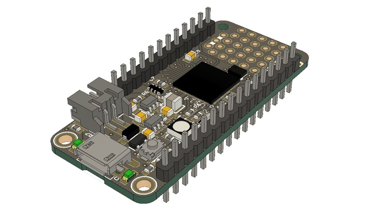
In this video I walk through the workflow of turning an adafruit board into a detailed 3D model. I use Autodesk Library IO to generate custom components to populate PCBs.
Adafruit CAP1188 Breakout
https://www.adafruit.com/product/1602
Adafruit CAD Parts on Github
https://github.com/adafruit/Adafruit_CAD_Parts
EagleCAD Download
https://www.au...
no written guide yet
PCB files for SCD-4x here: https://github.com/adafruit/Adafruit-SCD-4x-PCB
limpid nest
I'm looking at a design using the AW9523B, and I'm trying to figure out if it's safe for my micro to power the AW9523B at 5 V, but not level shift the SDA/SCL lines. Anyone know off the top of their head if this is going to cause me issues? It's not difficult to level shift those lines, for me.
let me find the datasheet
Had it up earlier
supple pollen
SDA/SCL should run fine with 3.3V pull-ups on SDA and SCL, the input high voltage is a minimum of 1.4V. The reset pin, however, could be problematic.
Thinking it over, reset should be fine too.
heavy jasper
Make sure the VoL of the AW9523B is low enough to register as a ViL low on the MCU as well (for SDA)
It might not pull it low too aggressively if it assumes it’s driving for a 5V-signaled ViL (which will be a chunk higher).
limpid nest
I was told elsewhere that the leakage back into the micro could be a big issue. I have a ton of board space so I may as well just level shift the i2c so I don't have to worry about it.
supple pollen
I wouldn't expect that over I2C lines, which should only be pulled down.
limpid nest
Hm? Do you mean internally? I've only ever seen i2c pulled up
heavy jasper
So - we were assuming the pull-up resistors on the I2C lines would be to the MCU IO voltage of 3.3V
The folks advising you about leakage may have assumed you were going to wire the pull-up resistors to 5V, which could indeed cause leakage if the MCU isn’t designed with overvoltage tolerant inputs.
madbodger was saying that assuming you tie the pull-up resistors to 3.3V, the AW9523 isn’t going to pull the lines up to 5V itself (it won’t drive the lines high, only drive them low).
limpid nest
ahhh I see
Ok I think I'm still going to use level shifting so I can just not worry about it. Why does anyone level shift if it's safe to just pull the bus up to the lower voltage?
I guess not all chips can trigger on 3v3
heavy jasper
Or if you need your 5V rail to turn on later than your 3.3V rail and you’re careful about power startup leakages.
limpid nest
Ahhh
heavy jasper
Proper level shifting provides some decent guarantees about each side not interfering with the other when unpowered.
limpid nest
How could they interfere with each other when they are unpowered? Or did you mean when one side is powered and another is not?
tough matrix
What is everyone's favorite P- and N-channel MOSFET for switching currents of 1-10 A (voltages up to 30v, Vgsth low enough for the mosfet to be fully on using 3.3v)?
Ideally in SOT23 or SOIC8 packages
I was using AO3400, AO3401, but they seem to be at end of life
 bright sparrow
unique patio
<@422953155039330305> You asked elsewhere:
> Not sure where this question would ...
bright sparrow
unique patio
<@422953155039330305> You asked elsewhere:
> Not sure where this question would ...
This is great.. thanks Danh
ember laurel
@tough matrix A&O recommends AOSS32334C
as replacement
I'm shipping a modified unit to EMI testing today. Crossing my finger.
Changes:
- Ferrite beads (420ohm@100MHz) on all wires going out the motor (3xphases, 2xLED)
- Larger ferrite core with 2 wraps (used to be small core with no wraps)
- 1nF capacitors from each cable terminal to GND.
- Slowed down mosfet switching by changing gate current to 20mA (source), 60mA (sink) (used to be 333mA source, 1A sink)
- Changed to newer buck converter - from SY8303A to SY21153AAIC
I can measure a slight improvement using near field probes. I definitely should invest in some more equipment to measure this stuff better, however.


had to put those beads inline with wires, using shrink wrap. New board will of course be done incorporating the beads.
 ivory jasper
Anyone have a kicad footprint for the Adafruit KB2040 Kee Boar? Just want the symbol for the pins and a footprint for the pinout (to make a board that uses it)
worldly schooner
ivory jasper
Anyone have a kicad footprint for the Adafruit KB2040 Kee Boar? Just want the s...
The footprint should be pretty close to that of an elite c? If you can’t find that, you could use a pro micro and tweak it to add the d+/d- pins.
ivory jasper
worldly schooner
The footprint should be pretty close to that of an elite c? If you can’t find th...
Yeah that's exactly what I was planning if I couldn't find a repo with the footprint in question
I'm making a tutorial and wanted to be able to point users to an existing repo but I'm not against making my own if necessary
I've decided not to use the Kee Boar anyway... The RP2040 just doesn't have enough analog pins for a normal-sized analog keyboard (what the tutorial is about). At this point I'm figuring that a Black Pill would be better... Even though it's a bit more complicated to use
worldly schooner
I’m also wondering why it doesn’t seem to exist, but it seemed like it was more intended as a pro micro substitute that I guess I never questioned it aloud.
How many analog pins do you need?
ivory jasper
worldly schooner
How many analog pins do you need?
Well, the design uses 74HC4067 analog multiplexers which have 16 pins each. This allows you to turn a single MCU analog pin into 16 analog inputs. So the RP2040 is limited to 64 inputs using this method. That means the biggest keyboard you could make would be something like a 60%
ivory jasper
The Black Pill has 10 analog pins (and they're all 5V tolerant which is great for beginners). That means it can support 160 analog key switches (Void Switches!). Or you could mix in some analog hall effect rotary encoders which use 2-3 hall effect sensors each
My latest analog rotary encoder design actually uses five sensors which might be going a bit overboard. The extra two sensors are to enable absolute positioning. So if you reboot your PC it'll "know" that you left that knob turned 90° 👍
worldly schooner
Is it necessary to have simultaneous reads? Esp32 s2 has two adc channels but it’s accessible on 10 pins each
ivory jasper
Th 5th sensor (or the 3rd in the "don't care about absolute positioning" style) is for adding pushbutton functionality. This gif should explain how that works: https://gfycat.com/fabulouscostlyblackrhino
 ivory jasper
worldly schooner
Is it necessary to have simultaneous reads? Esp32 s2 has two adc channels but it...
ivory jasper
worldly schooner
Is it necessary to have simultaneous reads? Esp32 s2 has two adc channels but it...
All that matters is the number of analog pins. Not the number of ACDs inside the MCU
The Black Pill only has two internal ADCs but 10 pins (strangely, only two go to ADC0)
The rotary encoder design is pretty nice: It's 3D printable and entirely contactless just like my Void Switches. You can lift it off along with the rest of the top plate (i.e. to go clean it in the sink): https://gfycat.com/enchantedmeageranteater
 worldly schooner
Oooooooo
ivory jasper
I'm using the Black Pill on that macro pad. It's all hand-wired! https://gfycat.com/delectableeverydoe

I released the Void Switch design files the other day (https://github.com/riskable/void_switch) so now I'm working on a board design tutorial. I really love the RP2040 because it's so simple to work with (any pin can do any function and PIO is awesome) but the limitation of only 4 analog pins is too much.

GitHub
3D printable magnetic separation contactless key switch and stabilizers (OpenSCAD files) - GitHub - riskable/void_switch: 3D printable magnetic separation contactless key switch and stabilizers (Op...
The PCB footprints and symbols for Void Switches are here: https://github.com/riskable/void_switch_kicad

GitHub
Kicad files for making an analog hall effect keyboard using 3D printed Void Switches - GitHub - riskable/void_switch_kicad: Kicad files for making an analog hall effect keyboard using 3D printed Vo...
It's really nice: If you set your "User grid" to 4.7625mm you can just drag & drop your keyboard layout around the PCB and everything will line up real easy
(4.7625 being 19.05/4)
(19.05mm being the standard "key unit" spacing)
proper anvil
Im creating an arduino uno clone (with some additional features) and i am trying to find what value the associated capacitors should be for the crystal I've selected, according to this guide (https://rheingoldheavy.com/arduino-from-scratch-part-9-16mhz-crystal-oscillator/) it should be specified in the datasheet. Is it the 'shunt capacitance' referred to in the datasheet?


trying to find appropriate values for C7, C8, which are 22pF on the official schematic but according to the guide it varies by crystal.
tough matrix
you need "load capacitance"
that is, you need
load_capacitance = C/2 +parasitic_capacitance
where C is the value of C7, C8 and parasitic capacitnace is capacitance of traces
proper anvil
Okay, if I make the traces very short can I ignore parasitic capacitance?
tough matrix
Or you can just pretend it is 5pF, as the RP2040 doc suggests
AFAIK, couple of pF one way or another won't make much difference
ivory jasper
Yeah I totally blew it on one of my boards once and added 22pF when it should've been 4pF. It still worked fine 😄
proper anvil
Oh okay, yes the link you gave is very clear. Thank you!
proper anvil
My intention is to integrate a motor controller IC on the arduino uno, in testing I found that having the IC connected straight to the digital pin all the time made it unreliable for purposes other than controlling the motor controller (I don't remember specifically, but I believe it was pulled high or low unintentionally). At the time I separated the motor controller with latching push switches, so it could be physically disconnected when not in use. But now im thinking could I instead use a voltage follower on each pin, exactly how the arduino controls the inbuilt LED?
the goal being that you can easily use the motor controller with pre-assigned pins, but if you don't need the motor controller, you can still use those pins as normal digital pins.
 queen skiff
anyone know what DC-DC converter I can use to do the 5-9-12-15-20V DC to DC conversion from a 4S battery pack?
 unreal flax
queen skiff
anyone know what DC-DC converter I can use to do the 5-9-12-15-20V DC to DC conv...
unreal flax
queen skiff
anyone know what DC-DC converter I can use to do the 5-9-12-15-20V DC to DC conv...
You'd generally want a buck-boost converter with selectable output via an I2C interface or similar. Maybe something like this? https://www.ti.com/product/TPS55288
queen skiff
that looks really good, thanks!
ember laurel
Good luck getting hold of one 🙂
fervent lance
I am working on a PCB design, based on the HUZZAH32 ESP32 board. Any suggestion what components I need to get 5V from a connected battery? (lipo or 18650) Should I just take the schematic from the https://github.com/adafruit/Adafruit-PowerBoost-1000C board and try to figure out how to connect it my schematic design?


GitHub
PCB files for Adafruit PowerBoost 1000C. Contribute to adafruit/Adafruit-PowerBoost-1000C development by creating an account on GitHub.
unreal flax
fervent lance
I am working on a PCB design, based on the HUZZAH32 ESP32 board. Any suggestion ...
Yes, that's probably a good approach, since you need a boost converter to do that, and the PowerBoost ought to be a reasonable design for that kind of circuit. You can also pick out a boost converter chip you like (TI has a good portfolio, for example) and based your PCB on the reference design in its datasheet.
limpid nest
In Fusion360, does anyone know how to set the location of a pin name in a symbol? You can see pin 1 on the left and 16 on the right, but together it looks like 116
 cinder anchor
limpid nest
In Fusion360, does anyone know how to set the location of a pin name in a symbol...
cinder anchor
limpid nest
In Fusion360, does anyone know how to set the location of a pin name in a symbol...
there's no way to align them?
 cinder anchor
are you sure there's no way to change the position?
I distinctly remember messing with that and figuring it out, but it was months ago, lemme see if I can install Fusion 360.
limpid nest
I did a bunch of googling. According to the forums, there isn't a way as of 2017. It's possible it got added in the last 5 years but I don't see a way
wow 2017 was 5 years ago. Time flies
cinder anchor
huh
why don't they have a Linux version?
firing up Windows VM
also, my gaming rig updated to Windows 11... I don't remember having a choice... ick
limpid nest
cinder anchor
why don't they have a Linux version?
Market share, I would suspect.
unreal flax
You can turn off the pin-number display, but I don't think there's a way to relocate the label.
limpid nest
That's what I'm finding as well. Very frustrating
tough matrix
fervent lance
I am working on a PCB design, based on the HUZZAH32 ESP32 board. Any suggestion ...
May I ask why do you need 5V? ESP32 by itself only needs 3.3V...
thick willow
I made a 3D model of a component in solidworks but when I try to render on Kicad it looks OK with OpenGL, but bad when Raytraced
Opengl VS Raytracing

 supple pollen
Looks like polygon orientation isn't correct.
thick willow
I looks liek if either some polys were flipped or 2 polies were zfighting
supple pollen
I like the shadows on the raytraced version
thick willow
yeah but if its an orientation issue, why would it render jsut fine on GPU? I would expect GPU to actually care about orientation and raytracing not much
what shadows?
When I open the file with fusion360 it renders just fine, I also tried to export it from fusion just in case it would fix it but no luck
any idea on how I could correct it?
for instance poly orientation (if thats actually the case)
supple pollen
GPU may not be doing orientation backfacing (this would make sense to me)
Look at the upper part of the curved metal bits in the lower cavities: in the raytraced one, their tops are dark.
I have no idea how to fix it in Solidworks, I'll admit my usual approach is to export it, then write a quick utility to go through it and clean it up.
thick willow
What about fusion? do they get exported fine?
fervent lance
tough matrix
May I ask why do you need 5V? ESP32 by itself only needs 3.3V...
To power WS2812B LED strips
thick willow
Those leds require a crapload of power
so unless you are using just a few and lightly, you wont get much batt life
the ESP32 by itself consumes quite a bit of power too
But assuming you already have all of that considered, you may want to use a DC/DC converter to get 5V and a level shifter
 dry jetty
I am integrating several mcu's on small motherboards, including Feather M4 and Trinket M0. I would like to supply them all from a 3.3V regulator supplied from a LiFePo4 battery (3.2V). The Feather seems to take either 5V USB or through its charger circuit to 3.7V battery. Does that mean that I have to give it 5V to the USB pin, or is there a neater way? I do not think the Feather 'understands' a LiFePo4 battery, but for safety reason that is chemistry I would like to use.
 inland hollow
On a board like the Adafruit QT Py ESP32-S2, can it accept 3.3V input on the BAT/GND pads? I wasn't sure if the voltage regulator would handle equal input as output.
I'd just like to solder a LiPo connector on for input.
unique patio
inland hollow
On a board like the Adafruit QT Py ESP32-S2, can it accept 3.3V input on the BAT...
Our boards almost always use a low-dropout regulator (LDO), so that should be no problem. That board uses an AP2112K-3.3, which is typical. It will not cut off below 3.3V: https://www.diodes.com/assets/Datasheets/AP2112.pdf
 inland hollow
@unique patio Thanks! I appreciate it!
 tough matrix
no, certainly not
Doesn't look like any JST connector I know either
Maybe some Molex?
 opal timber
Extensive online search for both are coming up dry. This is definitely a common part I've seen before, but don't know the name of it to save the life of me.
tough matrix
what is the pitch?
ember laurel
does anyone have a good recommendation on a reasonably priced linear regulator with good PSRR around 1MHz?
with 500mA+ current
limpid nest
Anyone know if a right angle jst should (stemma qt) port will fit in the footprint of a flat one?
Digikey just sold out of the flat one
twilit mango
limpid nest
Anyone know if a right angle jst should (stemma qt) port will fit in the footpri...
Does Adafruit make boards with both versions? Can check the board files. Not sure what you mean by "flat" versus right angle though...
limpid nest
I meant right angle. Sorry I forgot words. I just ordered from adafruit since I needed a stemma cable from you folks anyway