#help-with-hw-design
1 messages · Page 32 of 1
 flat vigil
 cedar salmon
what’s the best way to report hardware quality issues with feathers? I’m not rea...
cedar salmon
what’s the best way to report hardware quality issues with feathers? I’m not rea...
Post to the adafruit forum
cedar salmon
can i get a link?
 teal fjord
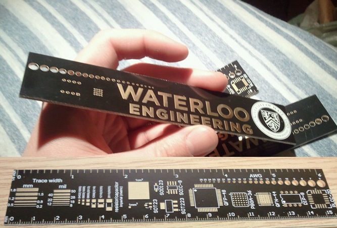
https://www.frank-zhao.com/pics/usbpcbbusinesscard/gold_rulers.png im gonna make one of these!!!! holy cow this is such a good idea!
 cedar salmon
thank you.
flat vigil
np
cedar salmon
We are hoping to Open source a large-ish scale project to universities in the nearby area mostly based on adafruit hardware
who’s the best person to talk to about getting a “kit” made available on the adafruit website?
Feel free to DM me if this isn’t appropriate for this channel
 flat vigil
cedar salmon
who’s the best person to talk to about getting a “kit” made available on the ada...
flat vigil
cedar salmon
who’s the best person to talk to about getting a “kit” made available on the ada...
Email support@adafruit.com
 spring moon
Does anyone know if the Adafruit's solar charger (https://adafru.it/4755) can function without a battery attached (just running off of live solar power and not storing it anywhere)?

This charger is the only one you need to keep all your Lithium Polymer (LiPoly) or Lithium Ion (LiIon) rechargeable batteries topped up. No matter the power source at your disposal! ...
 latent jungle
spring moon
Does anyone know if the Adafruit's solar charger (https://adafru.it/4755) can fu...
latent jungle
spring moon
Does anyone know if the Adafruit's solar charger (https://adafru.it/4755) can fu...
The datasheet for the bq24074 it is based on says:
This feature [DPPM] reduces the number of charge and discharge cycles on the battery, allows for proper charge termination and enables the system to run with a defective or absent battery pack.
https://www.ti.com/lit/ds/symlink/bq24074.pdf
So, seems likely.
teal fjord
Curiously when working with MCs and set ups that require power and ground on the other sides of my connects what is the best way to go about this?
Is it really just run a big long trace all the way around my board and hope to nudge it in some where?
Is it short stich vias? What about when I'm crossing my data lines with vcc on the other side of the board?
Is this what power and ground planes solve? If so where would I start learning to utilize them?
Am I dumb and should know where to find this information? I swear I have looked everywhere! I even resorted to asking AI, which gave a generalized dubious answer as always!
If there is a good book on the topic of PCB lay out id gladly grab a copy. What text book would a college class for designing PCBs use?
for refrence of what im talking about.

maybe I just use a usb c connector I bet that solves my whole problem and gives me access to ground and power on both sides of the connect. I mean it owuld have to cause its double sided... hmmm brb time to datasheet
 worldly schooner
teal fjord
Curiously when working with MCs and set ups that require power and ground on the...
worldly schooner
teal fjord
Curiously when working with MCs and set ups that require power and ground on the...
The general approach to two layer boards is really ground fill at the end, everything else is just mindful placement of components wherever possible. For some microcontrollers, you will have to short-stitch some vias, but there shouldn’t be any issues crossing power across the back of the data traces.
I’m pretty sure you’re overthinking this entire layout. My recommendation is to just put it all together first, then run DRC and ask about it afterwards.
And yes, four layer boards simply use inner planes for power and ground, which opens up a lot of space for more traces outside on both sides of the board.
 tough matrix
I usually start by doing ground pour on the bottom side of the board, the run traces as much as possible on the top and when it is not possible, jump to bottom using vias.
yes, placement of components is a key
worldly schooner
teal fjord
maybe I just use a usb c connector I bet that solves my whole problem and gives ...
USB C connectors are usually the same as or worse than their micro B counterparts. The connectors are often simplified to have a single row of pins, or have two rows of pins and you have to make connections to both sides.
teal fjord
Yeah USB-C was not the answer which I discovered.
I do feel like im over thinking the lay out, but not because of this specific design, but I feel like these problems im running into are a sign im doing something incorrectly or poorly. I look at other peoples boards and they seem really clean.
alos Hem, just for the note I have finished the board and run the DRC, it comes back clean, however it doesnt help me with like "pcb lay out theory", yes the board passes all the checks, but does that mean I did it right?
teal fjord
blah im just in my own head, I look at these multilevel high speed boards and im like "why doesnt mine look like that" and the simple answer is "it doesnt need to its not as complex"
worldly schooner
There isn't any such thing as a comprehensive "layout theory" from my experience. When it comes to these board layouts, nothing is a better teacher than practical experience. Sure, it may not be perfect on the first try, but even in a professional setting nothing ever is. It really is an iterative process where you make mistakes and fix them before letting your design loose into the wild.
Whether it's bodging wires or cutting traces, the first board is brought up to working before finalizing the design.
tough matrix
teal fjord
alos Hem, just for the note I have finished the board and run the DRC, it comes ...
do you want to share the final result so we can take a look?
teal fjord
Sure I was just thinking people might be sick of me by now and not want another screen shot.
This is the one i am happiest with. little things about it I dont like but I think thats just in my head and wont effect the real circuit.
Keep in mind this is before any sort of "function"
Today my goal is to try and create some pin break outs on the other side of the board and I think it will "done"

This board however should be completely programmable via usb with dfu program, I also plan on breaking out the IVR pins as well which are basically just SPI
Everyone has been really helpful and I apologize for all my dumb questions. I have this huge habbit of over thinking stuff
teal fjord
I sit down and im like "Im gonna Tony Stark the crap out of this" and then it takes me some time to realize I am not Tony Stark, more like Phoney Phart
 inland jungle
no decoupling caps?
 cursive sentinel
You need decoupling caps no matter what.
teal fjord
Alright apologies let me do some more digging around then and understand the concepts.
I see so I need a cap between the vcc in of the mc and the power supply
to filter noise.. weird I wonder why all the example circuits didnt include one 😐
This should be really realyl close to the vcc pin is my understanding.
This microcontroller techincally has 3 forms of VCC in.
It has a standard vcc in, then it has uvcc which is for the usb power side of it, then it has avcc (I forget if thats the real pin name) but it powers the analog features. Should I decouple all of them?
alright let me figure out about my circuit so I can figure out my decoupler values! Thanks everyone.
tough matrix
standard value is 100nF, placed as close as possible to each of VCC pins of the IC.
teal fjord
Thanks! I was having so much fun working this out!

One thing I need to do some research on is calibrating FQs, apparently I might have to calibrate my mc and the fq together. I was reading through algorythems for that last night.
one problem at a time decoupling caps
tough matrix
also: the datasheet tells that UCAP pin should be connected to external 1uF cap, but your board has 10uF - is there a reason for that?
teal fjord
I read that on the datasheet as well, which was a head scratcher but every single example circuit I could find uses 10uF
(I didnt make up this circuit its seemingly commonly online)
So my thoughts were that the designers of the circuits knew something I didnt know about something else in the circuit.
Upon doing my dudiligence on it, I still cant figure out why its 10uF but I am worried to change it
I even poured over teh data sheet trying to see if it was for some special configuration having to do with the usb....
cursive sentinel
tough matrix
also: the datasheet tells that UCAP pin should be connected to external 1uF cap,...
Usually pins named <something>CAP are driven by an internal charge pump circuit, so 10uF shouldn't hurt as long as the voltage rating is high enough.
teal fjord
Would there be a reason that others would use a 10uF other then its what they had in stock?
That was my other hunch was that 10uF was just more common and people were throwing what they had on there.
inland jungle
maybe can use cheaper caps without having to worry about derating?
teal fjord
id be ok changing it, I just havent because I didnt know any better
tough matrix
I think either 1 or 10 should be ok (as long as they are rated for 10V or higehr), I was just curious.
teal fjord
apologies for how sloppy it is, but this should do the decoupling capictors correctly right?
 cursive sentinel
Yes, although 10u is bigger than you want if you are using ceramic caps.
cursive sentinel
I believe @latent jungle has a video that covers decoupling basics somewhere.
teal fjord
Ok I will look for that video!
ok everything is 100nf now
and in right
Thanks for the help! Ill route these and then figure out what my next problem is
latent jungle
cursive sentinel
I believe <@312943079160283137> has a video that covers decoupling basics somewh...
actually, I don’t… I should though.
cursive sentinel
latent jungle
actually, I don’t… I should though.
Agreed.
teal fjord
I would watch it!
can you link your youtube channel anyway if thats ok?
Also to all the bro, broettes, and non-bronaries who do this for a living, my hats off to you, this is like waking up every morning to go do sodoku for a living!
could those two vcc pins share a single decoupling cap or is that a negative, because one pin would drain the constant voltage to fast?
 worldly schooner
While such compromises usually don't impact the overall function of the board, it's best to have separate capacitors per pin where possible.
teal fjord
thank you
latent jungle
teal fjord
can you link your youtube channel anyway if thats ok?
My channel is AddOhms. But here's a playlist of capacitor videos I have on other channels: https://www.youtube.com/playlist?list=PLRIGIzu0Z7KkJmYXS-OSRSbSxjk1yki_O
latent jungle
teal fjord
could those two vcc pins share a single decoupling cap or is that a negative, be...
I would use a polygon (or zone or copper pour) and connect those VCC pins together with a single large value ceramic capacitor.
teal fjord
I think I understand what that means, so like put a pad of copper down that connects them and run a cap between the two?
I apologize for my ignorance and I dont know if it means much, but I am trying to learn
latent jungle
Different microcontroller, but same idea:

in general, i avoid using traces for power. I draw zones / pours instead.
(or just use really wide/fat traces)
latent jungle
teal fjord
I think I understand what that means, so like put a pad of copper down that conn...
yes. use a big blob of copper to connect the two pins and a single cap.
teal fjord
wait I can do that?
Thats allowed?
all that copper wont mess up the signal or anything?
I can just take one big cap put it on both pins, fill that area with copper and be like come at me bro....
omg.... I feel kind of dumb.
man im dumb ok, let me try to figure out how to do this in my program! Thank you so much
what value for that cap would you recomend? The same as a normal passthrough?
latent jungle
for an atmega32u4?
teal fjord
yeah
latent jungle

 teal fjord
I am using the U2, the U4 has compitbility issues with some of the code im targeting
no usb power
wait
I am using the analog to digital converter
lmao
latent jungle
In that case, what I said about connecting the pins before and the same capacitor is completely invalid.
teal fjord
Tho in all honesty I am creating more of a test board then a board with a specific purpose, I plan to break out the extra pins on the other side of the board so I can play with stuff like spi and uart specifically
latent jungle
I was misled because they were both labeled VCC. (And it is common to have multiple supply pins.) But in this case, those are two completely different supplies.
teal fjord
I apoligize for that, that is my stupid program labeling the pins based on the net andnot what they are
I shoul dhave made that more clear and linked the schematic

 teal fjord
right htats what im doing
latent jungle
 teal fjord
ohh i missed that part.
latent jungle
VCC and AVCC should be connected with an inductor to form a low pass filter, but almost no one does that. Instead of what I said earlier, give AVCC its own 100 nF capacitor.
(in addition to the 10uF for VBUS). However, you don't need to the VBUS/VCC capcitor right next to the IC. That's what UVCC is there for.
teal fjord
Awesome! So I was closer then I thought
that above circuit in the data sheet is what I used to lay out mine. I did miss the highlighted part about the cap on vbus
Thank you for your help!
latent jungle
hold, I'll show what I would do. Since I'm all over the place.
@teal fjord if you have room and can route the other traces, something like this would be better: (UCAP is wrong, it shouldn't connect to +5V)

You really want pin 31 to have its own capacitor
latent jungle
ugh, that's not right either. 32 is AVCC.
latent jungle
At a minimum, you want this: (UCAP is wrong, it shouldn't connect to +5V)

C4=1uF for pin 31/32. 12uF for pin 27. And the nice big 10uF jut somewhere between the USB connector and the 32u2
lol anyway. I'm making way more of a mess than helping. It'll work fine.
teal fjord
alright im tracking this, now as far as my data out lines which would now cross the vcc is this an issue to use a via to route data to other side of board?
No you are helping!
latent jungle
On a 2-layer board, I would do something like this (but with fatter traces/pours for +5V lines): (UCAP is wrong, it shouldn't connect to +5V)

don't get too hung up on getting the imedpance and length of the USB lines right. for 12 Mbps and slower it is not as critical as people make it out to be. But you do want to have the ground plane (on the back side) underneath the traces unbroken.
teal fjord
ok
I think I understand
Yeah I understand
So another thing, with the idea of a ground plane I dont have to be all crazy about routing my ground lines back to the connector
cause when I fill in the ground plane it will be simple to connect what wasnt connected?
also I see its ok to route connections under the cpu socket too.. I was worried about that.
@latent jungle do you have a pateron or anything like that?
latent jungle
teal fjord
cause when I fill in the ground plane it will be simple to connect what wasnt co...
in general, yes. the only "routing" I do for ground is to a via next to the pin or pad to connect it to the ground plane on another layer.
latent jungle
teal fjord
also I see its ok to route connections under the cpu socket too.. I was worried ...
ideally, under a complex IC like a MCU, you want a clean ground on both the top and bottom layers. but, if you need to route some traces, do it on the top layer and keep the bottom layer as clean as possible.
teal fjord
omg if you guys werent so helpful the only thing Id manage to make is usb powered smoke bombs!
latent jungle
it's almost impossible to not route traces under a microcontroller on a two layer board.
teal fjord
omg ok I was thinking that too
I was even gonna write a "routing brute force" program to confirm it!
latent jungle
but when you do, do it like I showed above. super short loop.
teal fjord
ok epic!
ok one last question and I promise to leave you all be for at least another 30 minutes. Am I wasting my time learning on 1-2 layer boards? Should I be learning to do the fancy ground layers and stuff? Like am I "cheating" myself?
latent jungle
I think you mean should you be using more than 2 layers.
teal fjord
yes I think thats what I mean
latent jungle
There is probably little electrical benefit to going to a 4-layer board on a design like this one. It would make some routing easier.
But, learning how to optimize routes with a 2-layer constraint is a good skill to build.
teal fjord
ok then ill focus on building that skill first
I come from like coding, where a lot of learning stuff "gets things on the screen" but kind of teaches coders bad habbits, so I am just trying to avoid that kind of analog over her when learning electornics design
latent jungle
but I also don't want to be a curmudgeon that says: "well, I learned it this way, so you should too." If you want to take a shortcut to 4-layer, eh, fine. (but from a technical standpoint, there isn't a huge benefit to doing iit--in this case.)
teal fjord
My understanding is it also increases the fab price an acceptable amount as well?
latent jungle
four and six layer costs have plummeted. (the bigger is if you're using Eagle, the non-paid licenses only support 2-layesr)
teal fjord
Im using Fusion 360 cause I use it for my 3d printer stuff. Im not sure if it supports multi layers or not ill have to check
or rather more then 2
Im not overly opposed to spending money on software because I do plan to build lots of different boards
 deft sage
hi!
deft sage
my drc in easyeda says I have an error, but i cant see anything crossing


can you please help me?
teal fjord
It seems like your tracks are to small, it lokks like yours are 0.145mm and your constraints are set to 0.152mm min
deft sage
this is my first pcb
deft sage
teal fjord
It seems like your tracks are to small, it lokks like yours are 0.145mm and your...
how would I fix that?
just got told by the person who made the pcb tutorial that I can ignore that, thank you!
teal fjord
Ok first off im really new, so take what I say with a grain of salt, but
-
look at who you are gonna get to print your board, or the printer dpi that you are gonna use to make it yourself.
-
fine what the min trace width can be for the way you are gonna manufactor, if using like pcb way and stuff its on their site.
-
set your software to these constraints in the opitions.
-
When selecting your traces to run on the board, there should be a width selection, make sure it is above this constraint at least %5 to avoid flaws and stuff like that.
What the program over all is telling you is that it believes that your traces are to small to be created. It believes this cause its settongs are telling it to. You should believe those settings unless you have reason not to, IE the people making your pcb have machines that can make traces that small
@latent jungle video idea
"Day 1 introduction to board routing, gotchas, and explaining the ground plane"
teal fjord
Dear jebus I swear if you get me through this board I promise ill never look at another adafruit kit and go "i could do that better and cheaper".
teal fjord
Understanding ground fill planes really simplied the circuit!
I have a question tho @latent jungle on your examples I see that you ungrounded pin 27 the ucap pin and ran it through our big cap to the pass through to power. Was this a mistake? I fail to understand why you moved ucap from grnd to power.
I believe everything else tho is in order now


ahh I still gotta do the power light circuit
forgot all about that derp, oh well thats easy enough
teal fjord
by the end of this ill have a working board, or ill have usb activated smoke bombs.
Ahhh I can name my nets after my pins in my schem! Oh man that would have made stuff so much easier!
teal fjord
went over the 10 uf cap between ucap and ground and it was indeed wrong! I have no idea hwo that happened. I checked it several times vs 3 exadmple datasheets, and still inputed it wrong...
that is fixed from 10uf to 1uf
teal fjord
and the data file does say to ucap goes to vcc, but 5 example circuits i found when looking for how to do this all show it grounded.. hmm
latent jungle
teal fjord
Understanding ground fill planes really simplied the circuit!
I have a question...
yes. it was a mistake. it should go to ground. It should NOT go to +5V
teal fjord
ahh ok
im gonna trust yo on it
ok then I think we are gonna be good! I do have one last "worry" power in is coming from the usb connector towards the bottom (our big cap is off screen but there), this is technically the avcc pin...
So if I understand it right power is going from avcc, to uvcc, and then to vcc...
This seems backwards, is it going to matter that the usb and adc are powering up before the main vcc input on the chip? Nextly, will that 1 bypass filter work or do I need to rework the layout so that vcc is power, then uvcc, then avcc?
 latent jungle
teal fjord
ok then I think we are gonna be good! I do have one last "worry" power in is com...
latent jungle
teal fjord
ok then I think we are gonna be good! I do have one last "worry" power in is com...
I said wrong just now. UCAP goes to ground. It does not go to 5V
teal fjord
right i understand
latent jungle
it's connected internally in the IC to the power rail
teal fjord
Awesome. I did understand that part.
Tho I can see how reading the datasheet would have made you feel like it required power
teal fjord
also guys if you havent watched the bald engineer you really should!!!
Informative and funny af!
tough matrix
teal fjord
ok then I think we are gonna be good! I do have one last "worry" power in is com...
the time it takes for power to propagate over traces is so infinitesimal that it really is not a concern.
teal fjord
Thanks!!!!
I assumed that was the case but I didnt know if there was something special about power priority or something I didnt know
tough matrix
Just for future info, there are some situations where you want to delay powering a component until other components are fully powered. But this is done by providing appropriate start delay circuit (e.g. https://www.ti.com/lit/ab/slvaea3/slvaea3.pdf); some chips have such circuits built in and provide dedicated "soft start" pin. In any case, topology of traces doesn't matter.
In general, the chip datasheet will tell you if you need to worry about things like that. If the datasheet doesn't say anything about startup delays, then you don't need it.
(So far, I have never needed to worry about that - yet).
teal fjord
ok kewl so basically the datasheet will not assume I know things I dont?
thats what im always worried about with the datasheets, is like what if the creator is leaving something out assuming its common information... like dont power the usb pin until the main pin.
LIke I fear they expect me to have learned something in school that is "core"
worldly schooner
Again, none of this was anything I learned in school. It’s a practical subject where you learn complexities as they’re needed.
Past basic circuit rules, just try.
teal fjord
Right I feel like thats what I am doing. I was just explaiing why I asked about the power, because I was unsure if it was something that was "basic knowledge" or not thats all
 cobalt hound
Does this look correct? I'm using https://www.molex.com/en-us/products/part-detail/5033981892

 teal fjord
Anyone ever tried this instead of a connector? I was thinking this might reduce costs considering that the connector is a large part of the price of my board.

 oblique vale
I think Adafruit Trinkeys are made that way, with the PCB as the USB plug. it's definitely a thing some products do.
hard to tell from the photo, but note that the connector specs the outer contacts to be longer than the inner so that when you hotplug it, the power and ground lines are connected before the data lines to prevent damage.
teal fjord
Yeah, so the picture is from some one doing it for business cards, and their printed pcbs are set up with the power and ground pins longer for hotswap, but when he tins them it seems like a lot of it is cut off, the picture does show the outter pins slightly larger.
but yeah from my crap clipping it hsard to tell
I might try that, cause my boards are like 4.50 each and a large portion of that is the usb connector
https://www.adafruit.com/product/4870 ahh yeah they are like that!
 drowsy drift
teal fjord
I might try that, cause my boards are like 4.50 each and a large portion of that...
drowsy drift
teal fjord
I might try that, cause my boards are like 4.50 each and a large portion of that...
If you use a PCB footprint as a USB plug, you should go for the 2.0mm PCB thickness or be prepared to glue a small spacer on the bottom of your PCB to make up the necessary thickness. And if doing this for others, may want to add gold fingers option or at least ENIG finish to reduce oxidation issues with the connector
teal fjord
@drowsy drift thank you so much for the insight! For now this is for me, I mean I hope one day I could produce something other people might buy, but that day isnt today. This is all for my learning expeirences.
I was looking at oxidation problems with the finger connectors, and gold of course is very expensive. I think that is why a lot of people are tinning them with solder when I see them online.
2.0mm pcb thickness was a huge question I wanted to ask! So you tihnk 2mm and still need some sort of shimming?
drowsy drift
teal fjord
<@352910176736772096> thank you so much for the insight! For now this is for me,...
I think 2mm will work. I forget the exact thickness I used when I was playing with this, but the standard 1.6mm was definitely too thin
teal fjord
Yeah I remember a long time ago I got some kind of like kit project that had a 1.5mm board with the edge usb connectors and it was also problems for me!
Thats awesome! Do you happen to know where I could get some eagle cad footprints for it? I mean I think I could make my own but ive been getting bogged down in making so many components and footprints lol.
I dont even know what to google to get it 😐
nm i found one I think!
"usb direct edge connect" was apparently the proper terms
drowsy drift
teal fjord
"usb direct edge connect" was apparently the proper terms
You can also open up an existing Eagle design and export the parts from it as a library. So you could open up that Trinkey design in Eagle and get a proven footprint that way https://github.com/adafruit/Adafruit-NeoKey-Trinkey-PCB
teal fjord
ohhh! I didnt know that!
Thank you very much!
That solved another issue I was having! So man you just wrecked two problems with one paragraph! You rock!
drowsy drift
Limor rocks by putting so many of her designs up on github for us to learn from
teal fjord
yeah she does!
 quartz shadow
I have a question for everyone. I have 3 syringes of old solder paste that don't reflow correctly anymore. Is there anyway to recycle them, or at least keep them out of the trash? I thought about combining them, and casting them into a small trinket. Anyone have other thoughts?
teal fjord
Im debating on using these zigzag connectors invented by this dude named Albert. Seems like a pretty clever cat. The idea is that since the holes are slightly offset then you can plug a connector in and it will stay there cause of friction. Apparently its common as an AVR programer configuration (Type I), but it seems pretty clever to use for pin breakout as well

 hot otter
First time not using a premade arduino/RP board for a project, does this look like how it should be? going off the diagram attached and raspberry pi datasheet for the boards and sparkfun USB C breakout for the USB
https://datasheets.raspberrypi.com/rp2040/hardware-design-with-rp2040.pdf


 jade wedge
Someone want to tell me why my copper fills aren't filling in fully? If I move them away from the chip, they'll fill out more (though not 100% despite having corner smoothing off), but while they're in position they refuse to fully fill. I already turned the pad clearance down to .01 mm so they would stop getting blocked by the other pads, but they're now apparently interfering with themselves.
Also, if anyone asks, this is the prescribed method of layout that TI uses for this chip.

Also, is there a way to "hide" a component so I can't click on it normally? There's a battery holder that takes up the vast majority of the back side of the board, and I keep clicking on it while trying to click on other things.
Ahh... Never mind on the first question. It was a clearance issue. I had to change the clearance for both the chip's pads, and the fill itself. They were being blocked by that trace in the middle.
tough matrix
jade wedge
Someone want to tell me why my copper fills aren't filling in fully? If I move ...
for the second question, assuming you use KiCad, you can mark componet as "locked" and not allow locked components to be selected
jade wedge
Awesome. That will be super helpful.
tough matrix
right-click on component and select locking->lock
jade wedge
Yep, got that far, now just trying to figure out how to prevent locked items from being selected.
 jade wedge
Ahh, not quite what I was looking for. That only works for drag to select.
It's not a huge deal. Worst case scenario I just delete the battery holder until I'm done everything else.
Especially since this was the hard part. Did you know that reading the instructions is super helpful when trying to figure out how to layout all these components? It's like magic!

 ripe dawn
Miniaturizing capacitive soil moisture sensor
deft sage
Hi! Can someone please help me with pcb design? I'm trying to make a microsd to usb-c adapter, and I don't know where to start. (The top is SD, bottom is USBC, left is LED)

im really new to hw design, and I'm not sure if I need a microcontroller for this
worldly schooner
deft sage
im really new to hw design, and I'm not sure if I need a microcontroller for thi...
SD card readers are common enough of an application for single-chip solutions to exist for sale. You'll likely have to search for an IC that best suits your desired use case, but using an application-specific IC will save you from any programming requirements you'd otherwise need for a microcontroller.
I guess the first step would be to define your requirements as specifically as you can. What kind of USB connector and speeds do you need? What kind of SD card capacities do you need to support? I see a USB 2.0 Type C connector specified, is that what you need?
deft sage
I literally just searched EasyEDA's library until i found a component
I need it to be usb stick size
not insane speeds
but more than 30mb/s
it also needs to be compatible with mac
btw thx for ur help!
worldly schooner
Most SD card reader hardware should work with either OS; it's usually the driver or the card format that causes issues with one or the other.
deft sage
i thought because of thunderbolt and stuff
deft sage
worldly schooner
Most SD card reader hardware should work with either OS; it's usually the driver...
oh ok
worldly schooner
EasyEDA? I assume you're trying to source your components via JLCPCB for assembly then?
deft sage
yes!
worldly schooner
I thought someone else tried to make something similar. Have a look at the GL823K and see if that'll do what you're interested in. https://www.lcsc.com/product-detail/USB-Converters_Genesys-Logic-GL823K-HCY04_C284879.html

LCSC Electronics
GL823K-HCY04 Genesys Logic $0.3689 - SSOP-16-150mil USB Converters ROHS datasheet, price, inventory C284879
deft sage
what would I use it for?
can it convert the sd to usbc
if so, how do I connect them?
oooooh
reading the datasheet
i see what it does
how does it connect to usbc?
why does it have 2 vss

and what is a gpio pin?
oooooh led
worldly schooner
5V GND D+ and D- should explain themselves. CC1 and CC2 should connect to ground via 5.1kOhm resistors.
worldly schooner
Page 9 of the datasheet details DM and DP as D minus and D plus.
Make sure to connect both sides of the USB-C connector, or else it'll only work plugged in one way.
worldly schooner
As long as you don't connect DP to DM.
deft sage
ok
how do I connect them
it keeps crossing

can I do layers in scematic
its impossibke
ive turned them upside down
rotated them
nothing works
worldly schooner
No, you can either cross nets or use net labels. Nets don't connect to other nets unless the endpoint is placed on another net.
Net labels will connect a net to other nets with the same label.
 worldly schooner
Connector endpoints also count. If you pull the net one space to the right, you should be able to avoid that.
See Net Label, Net Flag, and Net Port. https://docs.easyeda.com/en/Schematic/Wiring-Tools/index.html
 worldly schooner
Yes, though I recommend for clarity to use net flags or move your wires off the component.
 worldly schooner
Connect 5V to both VBUS
and connect both VSS pins and GND pins to ground flags.
deft sage
ok, sorry bout late response
deft sage
worldly schooner
and connect both VSS pins and GND pins to ground flags.
what are ground flags?
ohhh
the supply flag thing
ok

done
how can I connect an LED?
like, do I just connect it to LED and ground?
deft sage
worldly schooner
and connect both VSS pins and GND pins to ground flags.
btw do I connect the bottom grounds too?
worldly schooner
Yes, all ground pins.
 worldly schooner
You may find your schematic will be cleaner if you use multiple ground flags instead of trying to wire all of them to one flag.
 worldly schooner
Missed one.
worldly schooner
I don't think VDD and VDDA are needed, but I could be mistaken.
deft sage
color coded!
 deft sage
worldly schooner
I don't think VDD and VDDA are needed, but I could be mistaken.
deft sage
worldly schooner
I don't think VDD and VDDA are needed, but I could be mistaken.
so am I done?
i still see gpio, and some digital pins
worldly schooner
Oh, https://oshwhub.com/H4lo/tf-ka-du-ka-qi-gl823k is an example of a working GL823k design. It uses a USB A plug instead of USB C, but the rest of the connections should make more sense looking at this.
基于嘉立创EDA进行电路设计的硬件开源设计大本营,集嵌入式、电子模块、DIY设计、物联网、智能硬件、电子应用、电工电子等多种电路设计模块为一体的开源硬件平台
deft sage
oh ok thanks!
uh oh
how do I connect the sd card to the chip?

since the chip to usb is done
worldly schooner
See the reference schematic provided.
worldly schooner
deft sage
how can I make them do the linking thing
worldly schooner
Just give two nets the same label, port, or flag
deft sage

i dont understand the parts in red
why do I need them, and can I ignore them
i dont realy want an LED
@worldly schooner
btw here is mine for reference
 worldly schooner
The capacitors help with the stability of the power supply. It might work without them, but having them will definitely improve system stability.
deft sage
ok, and how about the LED stuff
worldly schooner
The LED is probably an indicator for read/write activity, so you know if it’s safe to unplug. Totally optional.
The GPIO I don’t fully understand. The English datasheet doesn’t mention what it does, but the Chinese on the design translates to “GPIO pulldown for SD mode.” I assume you’ll want to include that, I have no idea what it does if you don’t.
deft sage
ok
teal fjord
Guys my board is getting there! Its really coming along nice! Everyone most def got me pointed in the right direction!
deft sage
cool!
deft sage
worldly schooner
The GPIO I don’t fully understand. The English datasheet doesn’t mention what it...
@worldly schooner i think im done!

here are of myu unfinished nets that im not sure about

i fixed those 2 VBUSs
 void tiger
I don't really know what I'm talking about, but doesn't it need a 5.1k resistors in cc1 and cc2 to request 5v?
worldly schooner
deft sage
here are of myu unfinished nets that im not sure about
5.1kOhm resistor from each CC pin to ground.
 hot otter
hey ur in the same boat as me xd
deft sage
wdym?
hot otter
trynna figure out USB C ports
hot otter
unfortunately mine goes past just USB ports
deft sage
wdym?
hot otter
trying to hook up a RP2040 directly
deft sage
ohhhhh
adafruit publishes all their scematics
check out the qt2040
it could give insparation for rp2040 to usbc
hot otter
oh right i forgot they do
i've got the board done pretty much im just checking with as many people as i can before i get it made
thats what Ive got so far


GND pins are connected I've just hid the GND copper layer
teal fjord
I think im doing ok! My board is most def coming along


I figured out how to make my schematics look good too
deft sage
oooooh
teal fjord
thats exactly what I said lol
deft sage
lol
teal fjord
im kind of to the point that im at design compromises. LIke deciding if I want to put pulldown/up resistors on my exposed pins, or manually ground them when I dont use them.
teal fjord
Most likely not but if you ask the question ill try to answer it.
teal fjord
I was looking at your circuit earlier and i dont know enough about the components to know if you are doing it right. Id have to pull the datasheets and read through them all.
deft sage
oh ok
teal fjord
I can tell you that nothing like jumps out at me as wrong, but that could just be because im to new to see it
deft sage
worldly schooner
5.1kOhm resistor from each CC pin to ground.
can I convert to pcb now?
the only pin I have left is 17
what DOES IT DO
HOW DOES THIS COUNT AS A DATASHEET

ITS A PIECE OF PAPER WITH SOME DRAWN OUT 3D MODELS
😭
teal fjord
yeah id call that an engeineer drawing more then a datasheet but its just a usb-c port so there isnt a lot of data on it besides dimensions
its more about what you "do with it"
deft sage
how do I know what pin 17 does then
its a paradox
if i order, im wasting money
but if I dont, how do I build it?
worldly schooner
17 I suspect is the mounting points for the outer shell. It's usually connected to a shield ground for mechanical support and electrical shielding. https://www.quora.com/Is-the-USB-metal-connector-shorted-to-negative-GND-pin-1

Quora
Answer (1 of 3): The metal connector — the shield — is connected to a “shield ground” or “chassis ground” inside your equipment. This will usually be connected to the main system ground — where your USB connector’s ground pin connects — through a filter (R/C or ferrite bead), and usually only at ...
worldly schooner
deft sage
if i order, im wasting money
Designing your own devices is usually an iterative process. While people do strive to make all the right connections, there is an expectation for errors to happen. People typically order their first boards, use a bit of handicraft to correct any errors, then edit the design with the changes to perfect it.
teal fjord
shielding is ground
worldly schooner
You probably don't have to worry about shielding right this second. A large resistor and a small capacitor between this and ground is the important part, not so much the shield ground symbol.
deft sage
so pin 17 > 1m resist > 1 uf > ground
teal fjord
@worldly schooner Im just about done with mine man! Its a large thanks to you and a few others here! I have the confidence to order my board and feel strongly I can trouble shoot any issues i might ahve after ordering!
 teal fjord
looks can be deceaving but its a atmega32u2 dev board.
worldly schooner
pin 17 > 100k resist > ground
pin 17 > 0.1uf > ground
worldly schooner
yup
teal fjord
i need to check my breadboard spacing and make sure that it can fit the rectangle ic package, and debate to myself about pull down resistors on my unused pins and fill my ground plane
worldly schooner
The values don't matter THAT much, but using less unique parts tends to save money in assembly.
teal fjord
This very true, when I went through and selected like parts that where common and instock it drastically reduced my price.

 worldly schooner
That's fine
deft sage
yay!
worldly schooner
Go play with the PCB layout stuff before you give yourself cold feet haha
teal fjord
I can attest to getting inside your head about it
it really is a proccess you have to expect illitrate through.
deft sage
i think im ready to convert!

i added a no connect flag to CD
just for the DRC
should I clean up my scematic?
or just leave it
worldly schooner
For future reference, you don't have to completely finish the schematic before you convert to PCB. If you need to make changes to the schematic, the updates will transfer over to some extent.
Up to you. If you're worried about messing something up, feel free to clean up later.
teal fjord
Im completley new but I really reccomend routing as you build the schematic. I have found it makes it much easier to decide where each part of the board should be... I dont know maybe this isnt how the pros do it, but ive found doing a part of the shematic, routing it, and then doing another part has made things way easier for me.
deft sage
worldly schooner
Up to you. If you're worried about messing something up, feel free to clean up l...
oh ok
teal fjord
(like my connectors, how can I know what pin I should put each connector to, until i route stuff and see what pins are closer to what connector port)
worldly schooner
I'd say it ultimately depends on the complexity of the board. For something like this with only three significant components, it really doesn't matter so much.
teal fjord
Also one thing that will save you a mile of headaches is set your DRC before you start routing... tho for your board it migh tnot matter.
worldly schooner
The GL823K is basically designed to be super simple for layout.
teal fjord
ahh nice!
worldly schooner
Just take it one thing at a time. If you get overwhelmed by the ghost lines, step back and connect the obvious dots first.
teal fjord
yeah all the ghost lines freak me out I start seeing them cross and think ill never get the board routed
worldly schooner
(but yes, for complicated designs, breaking it down by block makes layout a lot more manageable.)
teal fjord
have you ever used one of those touch buttons before hem?
are they half way reliable?>
worldly schooner
Touch buttons?
teal fjord
im not sure what they call them, but its basically a button with out the button stuff
 worldly schooner
Oh, those interleaving fingers
teal fjord
and it depends on your finger to bridge the contacts
worldly schooner
Never tried one bare like that, but they work surprisingly well with a conductive elastomer.
teal fjord
conductive butotn yeah
ok kewl
im gonna give it a try for this board, for the hwb (hold it plug it in, and it goes to program mode), if it fails its an easy fix to ground the pin when I want to program it
but its drastically cheaper then a button
worldly schooner
One of these days I should order a project... never actually found enough of a reason to buy one of my own boards after finishing a layout...
teal fjord
haha this one will most likely be long finished before I order it
my direct need isnt real pressing for it, but I have a whole host of pen testing expeirments I want to do with it.
It all started from this post I saw where a dude made a business card out of an atmega, where you plug it in and press ctrl 3 times on your normal kb and it prints a bunch of info out about his company in note pad (it assumes you have notepad open and cursored before pressing the ctrl)
and this made me wonder a few things, like first off is it that easy for usb devices to snoop on the line for key presses cause thats a bit scary, and also coudl you make a wierd "os" for a chip that uses note pad as your temrinal screen,.
worldly schooner
Oh yeah, lots of fun PCB business card designs out there.
worldly schooner
One guy built a small but functional Linux system on a card
teal fjord
thats my long term goal is to make a small sbc
Im realizing that goal is much further away then I thought it was
but doing research I have the schematics to like the orange pi, and its not out of grasp just take me a while to get the skills required.
also i think it would be fun to order like 100 of these boards and do a distrubted computing experiment as well
worldly schooner
An SBC isn't too hard until you try to beef up the performance to the point of a GUI
teal fjord
yeah I could see that but for me, I would be just fine with like 333mhz (my first computer ever) with like 8-16 megs of ram ever
worldly schooner
https://www.thirtythreeforty.net/posts/2019/12/designing-my-linux-business-card/ if you're interested in something SUPER simple
Behind-the-scenes build log for my Linux-powered business card
teal fjord
Hem your usefulness in this community can not be understateed
dude this is like exactly what my goal is!
worldly schooner
I just pop into conversations where I have some personal (or professional) interest. Pay me no mind.
teal fjord
lol
worldly schooner
Hm? Didn't you already select capacitors?
deft sage
yeah
worldly schooner
OHHHH
deft sage
turns out they are gigantic
worldly schooner
Hold on
deft sage
 teal fjord
https://linux-sunxi.org/F1C100s tihs one chip is better then my enter computer!
deft sage
chonky
teal fjord
Those are some big ceramic caps...
deft sage
yeah...
worldly schooner
Yeah you probably picked a tantalum capacitor by mistake. I believe you're looking for the MLCC category.
deft sage
how do I find one
ive searched
nothing
only 0.1 pf
and yes, i have a up facing usbc
thats by accident
and im too lazy to rewire
worldly schooner
Ah. 0.1uF = 100nF.
teal fjord
Ive been using 0805 footprint
worldly schooner
Try that instead.
worldly schooner
There are a surprising number of equally or more mindblowing chips floating around these days. This is just scratching a surface of the possibilities of ICs.
An SBC, like any other electronic device, is only as hard to make as you define it to be.
teal fjord
Thats very true, but ill be honest when I was looking at sbc i was basing my research off hte PI stuff, I never thought to just look for lower power chips
worldly schooner
There's a bunch of Pi-Pico-sized Linux SBCs floating around today, and the main downside is software support.
https://wiki.pine64.org/wiki/Ox64 is one such device. If they manage to release a stable OS for this thing (spoiler: they probably won't) it could be worth exploring.
PINE64
teal fjord
Well OS is tricky but if I can bet a board together that takes minimal porting of the os to work (like how this dude with teh business card describes his experiences) then after that I believe I have the skills and experience to do whatever I want. I can write drivers and stuff so.
whats keeping them from a stable os?
I imagine they are having wireless and wifi driver problems cause a huge portion of them are closed source.
worldly schooner
Okay, I misunderstood. The OS exists, but you have to build it yourself from buildroot.
teal fjord
ahh good ol build root
worldly schooner
It's a bunch of missing drivers as well.
teal fjord
yeah I could imagine that. The biggest hurdle of a new os flavour is the core drivers you need in modern day
cause a lot of them are closed sourcer.
like bluetooth and wifi are nortiously hard to support
 supple pollen
After some annoying experiences with bluetooth, I just don't bother with it. For WiFi, I just stick on a WiFi module.
teal fjord
^^^ my experiences too brotha
worldly schooner
Good old M.2 modules or ESP32s for days.
teal fjord
the ESP32 is a nice board ive been looking at it, and ofr any real project I would def target it, but the point of me making these boards, is like to learn ot make these boards.
but the esp32 is a solid buy imho
supple pollen
Last time, I used a TI CC1100 module I think
teal fjord
just pulled the datasheet for it(learning to do that)
You write the driver from sratch?
deft sage
what does the ground stuff in the scematic do?
worldly schooner
Connects them to the other ground stuff.
teal fjord
it grounds out your circuit of course. THats what the gnd pin on your usb port is for 😉
worldly schooner
Voltage is relative, and ground is (usually) your point of reference.
teal fjord
supple pollen
I found a driver library for it in this case, which helped
teal fjord
very awesome dude!
deft sage
I think its ready!
i tried to line up my components
autorouted
and there is zero DRC erros
teal fjord
well all thats left is full send right?
oh man and this guy has a genius idea so I dont have to make my pcb thicker!
 swift path
https://www.adafruit.com/product/3589 Adafruit PiUART - USB Console and Power Add-on for Raspberry Pi, can i use 2 of these on PI5?

Here's another super handy add-on for your Raspberry Pi computer, perfect for 'head-less' setups! The PiUART adds a USB Type-C to serial connection so you can use any serial port ...
 unique patio
swift path
https://www.adafruit.com/product/3589 Adafruit PiUART - USB Console and Power Ad...
unique patio
swift path
https://www.adafruit.com/product/3589 Adafruit PiUART - USB Console and Power Ad...
because you want two USB ports? There is only one serial connection, and they will fight with each other for this.
 woven bluff
can something like INA300 good for GM counter?
threshold is simply adjustable by DAC
 teal fjord
When you dont consider your board dimensions properly and your breadboard is miss aligned with no room to fix it 😦
supple pollen
woven bluff
can something like INA300 good for GM counter?
What is a GM counter? Threshold for what? Comparator?
teal fjord
I had to look it up hes making a device that detects radiation
Giagiar meter or whatever... I cant spell it correctly
or at least my googles lead me to believe these.
teal fjord
If any of you ever meet George Hilliard be sure to mention that his awesome article on his linux business cards is so informative! Its nuts!
woven bluff
supple pollen
What is a GM counter? Threshold for what? Comparator?
Geiger-Muller counter
supple pollen
woven bluff
Geiger-Muller counter
No, I don't think that would be useful. A G-M tube produces tiny pulses of current, the usual approach is to AC couple them (to remove the high voltage bias) and then just have a simple pulse detector.
inland jungle
yeah, with ample amplification and pulse shaping
teal fjord
ample amplification.. i see what you did there.
swift path
unique patio
because you want two USB ports? There is only one serial connection, and they wi...
makes sense thank you
woven bluff
supple pollen
No, I don't think that would be useful. A G-M tube produces tiny pulses of curr...
pulse detector detects voltage, I don't see how you can not have a shunt resistor in the solution
IN300 has a current sense amplifier, a compactor, and a schmitt trigger in one package
inland jungle
does it have pulse stretcher? can it handle the high voltages in a G-M tube? datasheet looks like a 10us minimum time response, doubt that's applicable
there's plenty of circuit diagrams for a G-M counter if you're interested in how they work and what they look like
supple pollen
The IN300 is designed to sense large currents at low frequencies, but G-M tube outputs are low currents at high frequencies.
There is normally a shunt resistor, yes: to convert current into voltage. You can also use other approaches (inductors, transimpedance amplifiers, etc.).
 hasty solar
is there a way to send an adjustable (reduced) voltage through a circuit that's cheaper than a buck converter? trying to make the voltage at the control pin of a 555 timer adjustable in a device I'm building so it can be calibrated to the voltage produced by an analog sensor
is setting up a voltage divider with a potentiometer and very high resistance a bad idea, since it'd involve sending continuous live current straight to ground?
cursive sentinel
hasty solar
is setting up a voltage divider with a potentiometer and very high resistance a ...
It is a bad idea, but not for the reasons you think. Which 555 are you using specifically?
hasty solar
would need to look up the specific model, it's the chip included with sparkfun's beginner kit
parts listing just says "555 timer," pictured on the left here
 cursive sentinel
Long story short, 555s tend to struggle with both very large and very small component values. The output is also going to be heavily temperature dependent unless you choose your components carefully. It isn't really something that you can just calibrate once.
LM555. That's an old one.
The datasheet should say what resistor and capacitor ranges are acceptable.
-# Probably something like 1k-680k for resistors and 10n-1u for caps
hasty solar
dang I was looking at a few mF based on the math I was doing. this is the diagram I had put together, not including the voltage control I'm talking about here

the goal being configurable on/off cycles between a few seconds and a couple of minutes based on the two potentiometers
supple pollen
You're probably better off with a different solution (I'm thinking an 8-pin microcontroller with a very simple program)
hasty solar
yeah I'm a software engineer and already have a couple of micros sitting around, I'm just trying to build this system with circuits as a learning exercise
cursive sentinel
Yeah you aren't going to get 555s to work consistently with caps that large. Keep in mind that 10% tolerance is considered "good" for most types of capacitor.
supple pollen
There used to be chips that included an oscillator and a bunch of binary dividers to provide long periods with reasonably sized components, but I think they're obsolete these days. But you can still lash up a separate oscillator (555 or other) and a counter chip.
Maybe look up the older chips like CD4060, MC14541, CD4536, and even the combined 555+counter chip CSS555
 brittle shard
Is there a board datasheet for the RP2040 LoRa?
supple pollen
Not sure what you're looking for. The product page has the specs, the learn guide has the pinout and detailed information, and the board files are probably on github
 mossy acorn
If I have an analog input that could be disconnected, should I add a pull-down resistor so that it doesn't potentially read random values when the input is floating(disconnected)?
woven bluff
supple pollen
There is normally a shunt resistor, yes: to convert current into voltage. You ...
why haven't I thought of that? TIA is exactly what I need.
supple pollen
mossy acorn
If I have an analog input that could be disconnected, should I add a pull-down r...
It depends on whether it's a problem to read a somewhat unpredictable value. A pulldown (or -up) resistor will tend to make it consistently read a low (or high) value with nothing else connected, but will form a voltage divider with the input when something is. As long as your analog input is enough lower impedance than your pull resistor, it shouldn't make a big difference.
teal fjord
The pull up resistors of arduino used to annoy me. Then I designed my own board and learned why they were there lmao. Designing my own board really taught me about why a lot of of the arduino is the way it is lol
supple pollen
Oh yeah, we can learn so much doing something like that!
teal fjord
I have learned so much, but I think the biggest thing that I learned was that these boards are "made the best they can be, with compromises made for flexibility". I used to think that some of these things "could be better and they just don't know how to code good", but it couldn't be further from the truth. Manufactoring concerns ALONE are enough to understand why the boards are the way they are.
supple pollen
Weird things like the 1k series resistors so you can use the UART without interfering with the USB-serial chip made me roll my eyes until I understood the philosophy behind it.
teal fjord
EXACTLY!!!
Or like on the pi zero why they have a usb port for power and one for data, why didnt they just combine them like all the big manufactors... OMG i know why... I freaking knowwwwww!
Oh why is the arduino uno so big... surely thats just cause they want the noobs to see what everything is, they could make it smaller if they wanted to.... and I learned of course they could... for tripple or more the price!
Ive also learned that bench power supplies are way worth their money... I had no idea....
supple pollen
Yeah, I made do without one for way too long
teal fjord
Yeah ive been looking at some, thinking about picking up a cheap starter one.
 waxen halo
I kept telling myself I'd just make one and then never finished the design, finally broke down and bought just last week one. Immediately helped me diagnose an issue I didn't understand. Always just got away with USB power or one of those breadboard sized supplies.
teal fjord
yeah thats what ive been using, but its getting to the point where I want to know more. I want adjustable power, you know kewl things like that. I even have convert an ATX power supply to a desktop power supply, but i worry about using it to power stuff I dont really know about cause it doesnt have any "real protections", so a good desktop one would bring a lot of confidence.
waxen halo
My design was just going to be a very custom front end to an atx supply. I will still probably make it, but having a "reliable" one around is very nice.
My poor monitor that usually supplies the USB power has probably seen some things
teal fjord
Yeah that was my orginal intent as well, and then I started doing all the research for it and did some simulated circuits, and I feel like I could "make one" but i dont think it would improve my confidence in one.
lolol
waxen halo
Unrelated: If I have some exposed (low power) connections close together, is it safe to just cover them in hot glue? Searching seems to indicate it probably won't conduct.
teal fjord
ive seen hot glue used to do that before but I don't have experience with it myself
teal fjord
This is gonna sound like a dumb question maybe... but im inside my head so humor me. Is it kewl if I ground two differnet voltages out to the same grounds? If voltage is realitive wont grounding say 3.3v and 5v to the same place change that realitivty?
inland jungle
you almost always ground to the same location, in fact that's one way to ensure that the 5v and the 3.3v have the correct relative voltage
teal fjord
Outstanding, then I did it right! I was just suddently worried that I needed seperate ground planes for my voltages
inland jungle
yeah, sometimes you want separate ground planes for analog signals and digital signals, for example, but even then you usually tie them electrically together at a single point
teal fjord
AHh ok that makes sense why I seem some of the more advanced boards with different ground planes for differnet stuff!
Thank you Kevin!
When skynet takes over the world I will be sure to give you an island of your choice 😉
inland jungle
appreciate it
teal fjord
Wow I just learned there is a whole programming language for designing like ICs and stuff! Like microchips! Its done with a freaking programing language!!!
latent jungle
You mean HDL?
teal fjord
Yeah I think thats one of them I was looking at, apparently there is like two big ones but I am still learning the details.
latent jungle
HDL isn't a specific language.
teal fjord
lol ohh
worldly schooner
HDL is Hardware Design Description (oops) Language, VHDL and Verilog are languages of HDLs.
teal fjord
ive known this exists like 20 minutes so humor me a bit 😐
ahh ok the verilog is the one ive been looking at yeah veriglog!
verilog*
if you would have asked me how microchips where deisgned and given me 1000 guesses I would have never guessed a programming language lmao!
worldly schooner
Well, they're one way to design chips.
latent jungle
well, "programming language" isn't correct either
teal fjord
I guess thats true "programming language" doesnt really fit you arent programming anything, but yeah.
latent jungle
it's almost like there is a "hardware description language" to define how hardware is described, in some kind of language.
worldly schooner
I mean, you technically CAN program a chip with Verilog or VHDL.
Oh fffs did i misremember the acronym
That's on me.
teal fjord
latent jungle
it's almost like there is a "hardware description language" to define how hardwa...
yeah im only looking over some basic stuff an lc3 design because ive done an lc3 virtual machine before... it just blew my mind it worked this way. I dont understand a lick of it yet but its still nifty.
latent jungle
I have zero clue (or interest) on what lc3 is
teal fjord
it stands for little computer its just an arcitecture specifically designed to teach computer science. It has very few opt codes and registers.
deft sage
@worldly schooner can you please help me design a dev board for rp2350?
@hot otter u r making a rp2040 dev board right?
if so
im sorry
deft sage
deft sage
<@98211350907490304> can you please help me design a dev board for rp2350?
specifically using a rp2354b
it has more pins
deft sage
deft sage
https://datasheets.raspberrypi.com/rp2350/hardware-design-with-rp2350.pdf
this datasheet-like thing is super useful
i wanna make it super specced out
TONS of flash and sram
like maybe 16mb sram and 32mb flash (if possible)
i can cut in half for 8mb and 16mb if needed
this will be super cool when im done!

more sram is possibleeeeeeeee
YAAAAAAAA
flat vigil
deft sage
like maybe 16mb sram and 32mb flash (if possible)
have you found a 16mb psram chip?
deft sage
im going to try 2 8mb chips in series
worldly schooner
deft sage
<@98211350907490304> can you please help me design a dev board for rp2350?
I honestly couldn’t offer you anything past the hardware design guide you seem to have found already.
deft sage
flat vigil
and no external flash?
i said
32mb flash (if possible)
sorry if i wasnt clear
deft sage
worldly schooner
I honestly couldn’t offer you anything past the hardware design guide you seem t...
oh ok, but for basic stuff can u still help?
worldly schooner
In fact, my recommendation for newer hardware designers would probably be to use an existing design as a basis. As the metro and feather designs have yet to be published, I can’t even link those.
flat vigil
deft sage
32mb flash (if possible)
I don't know how you attach 2 psram and a flash
 brave vigil
deft sage
specifically using a rp2354b
brave vigil
deft sage
specifically using a rp2354b
Why wouldn't an existing RP2350B board work for your use case? https://shop.pimoroni.com/products/pga2350

A minimal but powerful RP2350 breakout board modelled on a Pin Grid Array, with the maximum exposed pins crammed into the smallest possible space.
deft sage
brave vigil
Why wouldn't an existing RP2350B board work for your use case? https://shop.pimo...
much much harder to source, im doing pcb fab + pcba
teal fjord
@brave vigil thats really kewl i didnt know that existed!
and stuff with Raspberry Pi on the name can be super hard to source. I have ran into that myself.
brave vigil
deft sage
much much harder to source, im doing pcb fab + pcba
Just solder male pin headers underneath the PGA2350, and get PCBA for female headers somewhere on your board. It should just slot in, 🤞
brave vigil
deft sage
they dont stock the stamp
I mean purchasing the PGA2350 separately, and soldering a bunch of male header pins to it. After the soldering, it shouldn't be that difficult to place the PGA2350 assembly into PCBA-ed female headers on your board from a place like JLCPCB.
brave vigil
deft sage
much much harder to source, im doing pcb fab + pcba
I guess the cost of a soldering iron would be too much with my idea. If there's a local makerspace in your area, they might have the tools necessary.
deft sage
I have a soldering iron and stuff, it’s just a better goal for me to design end to end
And to get it fully manufactured
teal fjord
Are you planning to make a lot of this board or just one?
brave vigil
teal fjord
Are you planning to make a lot of this board or just one?
I didn't think of that. Yeah, it would only be feasible if they were making at most, a few units.
teal fjord
Yeah I learned my lesson on that. I designed my board with the idea ill just send it off and have it fully made.... sheesh... the cost of a fully assembled board I could by litterally 6 pcbs and all the parts to build it my self.
If you arent planning to order a decent amount of boards, it really isnt feasible to design with the idea that all of them are just gonna be manufactored at the factory
brave vigil
teal fjord
Yeah I learned my lesson on that. I designed my board with the idea ill just sen...
Oh, I was thinking about the time to solder 64 male header pins. I didn't consider that.
teal fjord
Oh yeah and if you have any through hole parts... omg you better kiss your reasonable price good by!
Now if you need 10 of these boards, thats a real big difference then the price starts to justify the time it takes you to build ten of them.
I designed what is basically a less impressive arduino uno and its cost assembled its more then just having purchased an arduino uno
unassembled tho aand its drastically cheaper, like maybe 4 dollars or so...
Also another thing to remember is most of these places use a flat rate shipping charge, so paying 20-40 dollars to have 1 little pcb shipped to you, its also insanity
 distant raven
worldly schooner
In fact, my recommendation for newer hardware designers would probably be to use...
distant raven
worldly schooner
In fact, my recommendation for newer hardware designers would probably be to use...

GitHub
Open source repository for storing the files for the RP235X-B Evaluator, an RP235X-B Evaluation board. - Oak-Development-Technologies/RP235X-B-Evaluator
you're in luck lol..
worldly schooner
distant raven
https://github.com/Oak-Development-Technologies/RP235X-B-Evaluator
You usually do your own assembly, right? Are you planning to try a couple of different combinations of FLASH/PSRAM?
distant raven
I am, or I'm going to try anyway
most psram won't fit on the second footprint but it appears the one that Adafruit sells (the espressif one) should (fits the phyiscal size parameters of the QSPI Flash i've chosen)
128Mbit, 16MByte QSPI primary and secondary FLASH for the initial prototype I intend to make.
I use a 5x6 WSON. I haven't verified the footprints are the same though so we'll see.
hot otter
deft sage
<@206085226709909507> u r making a rp2040 dev board right?
kinda, its a keyboard but using the schematic for the dev board
 thin falcon
What is the difference between these two ESP32-S3 variants? 8MB Flash No PSRAM Vs. 4MB Flash + 2MB PSRAM. As a circuit python user, where/when will I notice the difference? Some kinds of code? Some applications/use-cases? some driver compatibility? Performance? Speed?
supple pollen
More RAM lets you run more complicated programs (more libraries, more data)
flat vigil
thin falcon
What is the difference between these two ESP32-S3 variants? 8MB Flash No PSRAM V...
Right now the 4MB flash versions won't have BLE support and a few other things. 8MB has a larger partition for CP code than 4MB.
PSRAM is helpful for holding code
 scarlet jay
Supsup
Can I use X9C103 in 15V input if I want 20V AC output?
Or in general, Can i use any digital potentiometer?
cursive sentinel
Without knowing more about your application, I can't say. In general though you don't wanr to be using digitpots to produce a waveforms. A regular DAC will do it far better.
worldly schooner
scarlet jay
Can I use X9C103 in 15V input if I want 20V AC output?
No, the digital pot terminal voltages max out at +/- 5V according to the datasheet. 15V would be too much.
Usual approach for a high voltage signal would be a DAC and an amplifier circuit.
If this is a power conversion, you'll want to use a transformer or an inverter, neither of which utilizes pots or resistors.
scarlet jay
@worldly schooner thank you, thank you, thank you - i'll try the DAC approach although 555 and Pot would do atm as i come from 15v already to 555 (tried BD9555 but IT is uncertifiable)
scarlet jay
Because I have DAC in XIAO SEEED NRF52 Module but I only found LM2705 that takes it to 20V but I Don't think it transfers frequency.
 inner rampart
I"ve got an esp32 board with this charger chip in it. The switch on the board only switches the battery power on and off but I want to use the switch to turn the board on and off during usb power. So i'm wondering if I connect usb 5v to the battery plus pin will the chip let the magic smoke out or just kinda work ? https://github.com/Xinyuan-LilyGO/T-Display-S3-Long/blob/master/datasheet/SY6970 .pdf

GitHub
Contribute to Xinyuan-LilyGO/T-Display-S3-Long development by creating an account on GitHub.
supple pollen
Chances are it would destroy the charger. What I'd do is cut the USB power trace and splice a switch into that.
ripe dawn
Detecting AC Voltage
 ocean coyote

does anyone know what this might be a breakout for? Prog got cutoff a bit

also is it possible to have a device transmit a signal and recieve it on the other end over a single core?
kind of like those ac voltage detectors
but without the dangerous ac voltage 120 or 240 etc
supple pollen
It looks a little like a programming port for a flash chip, but those are pretty generic signals and could be for a variety of things.
Not sure what you mean by a single core: like a single wire?
There is a slightly related discussion here: https://discord.com/channels/327254708534116352/1273686414579466350
ocean coyote
supple pollen
Not sure what you mean by a single core: like a single wire?
oh sorry like solid core*
supple pollen
Still not sure what you mean
ocean coyote
i was thinking of a different msg i was talking to someone else abt my bad
let me draw it up
so i want to have a transmitter and a reciever and be able to go around finding if somthing is connected

but with a single wire
unlike how a contunity test would work
or data tone tester
ocean coyote
supple pollen
There is a slightly related discussion here: https://discord.com/channels/32725...
so its kinda like that ac voltage detector
so im guessing it would need a reference like using contact with human skin as a capacitor
 supple pollen
That pretty much is a data tone tester you're describing
 lone basalt
Hey folks! Could I get a quick review on this schematic?
It's a wireless bridge for the original Xbox
The important parts are the W5500 and the ESP32-C6. The weird Xbox stuff was taken from the rev 1.6 schematic that you can find online
ripe dawn
Rotary encoder with 5-way nav
 gritty sigil
hiya folks 🙂
Is it okay to power up the esp32 feather v2 (id 5400) via the bvus and gnd pin using for example a sbc, if you never ever plan to usethe usb-c port, and use for example a buzzer and otherwise only serial communication? As I understand it, the only risk when powering from 5v this way is for the usb-c port to be a danger because you might accidentally backpower it by mistake. But couldn't I use a diode to prevent this just in case?
supple pollen
Yes, a diode is the usual approach
gritty sigil
do I need a specific kind of diode?
supple pollen
Any diode that can handle the current and voltage will do. My usual choice is something like a 1N4001 or a 1A Schottky diode to reduce voltage drop in the diode.
gritty sigil
oh good I was planning to use that but didn't know if it was correct
supple pollen
Since it's just feeding a 3.3V regulator, the voltage drop in the diode means the regulator doesn't have to dissipate as much power
gritty sigil
yeah, I might go with that then
so that would let the usb-c port work for debug purpose while not allowing power, no risk?
supple pollen
Wait, I'm wrong. Having a diode there would avoid having USB backpower your supply. In order to avoid having your supply backpower the USB, you'd have to modify the board 😦
gritty sigil
hmm. I guess an alternative could be a switch to cut power to the vbus pin of the board, so like flip the switch and the power sent from my sbc to 5v vbus/gnd cuts out, so that I can plug the usb-c cable that would provide power and data, could that work instead?
hopefully my project would go well enough that I could ultimately not need to debug, but having the possibility of doing so while avoiding taking down my entire circuit or even part of it would still be good
I'm actually working on building a uart to wifi bridge. I've done it successfully with esp8266, but also want my project to have compatibility with esp32. So the idea is you connect the uart of the esp to the pins of your board or any other hardware that uses serial, and this gets exposed over the network on tcp. Extremely useful when you want to debug a failed boot on a sbc you have no easy physical access to
supple pollen
That seems like a useful device
gritty sigil
huh huh. I plan on publishing the code on github or something so others can use it 😄 it just is in need of quite a bit of refactoring first
one of my reasons for adding esp32 support is also that esp8266 is very limited. I have no way of debugging my project over serial for example, since that would mess up the serial on the sbc side of things
but with esp32, since debug is on its own serial, there's no such problem
supple pollen
These days, "thow more hardware at it" is a completely reasonable approach
gritty sigil
hehe definitely
I hadn't realized the second uart on the esp8266 is tx-only, or I'd have gone straight for esp32 :/
you also cannot shut up the boot rom that talks at 74880 baud on the first uart
worldly schooner
If you’re capable of soldering to the board components, there is a node VHI you can direct your diode-protected power source to.

The node is labeled because it also connects to the second regulator for the stemmaQT port.
gritty sigil
I might ask the adafruit distributor I'm getting things from to solder things on for me. I can't solder on my own due to motor disabilities and total blindness
oblique vale
gritty sigil
I'm actually working on building a uart to wifi bridge. I've done it successfull...
this sounds a lot like esp-link. I was going to use it years ago to add wifi to an old LED sign, never finished the project. esp-link looked like a great wifi-serial bridge firmware for the ESP8266, though.
gritty sigil
it did, but it also felt bloated, to me. Because it did more than just focusing on serial bridge. I didn't need an http server, a thing to do mqtt, etc. All I really needed was the serial bridge
the only stuff I have in my project is a transparent uart to wifi bridge, an admin console using telnet protocol where you can change settings from their default and they get stored on an emulated eeprom, and messages from the esp sent over network via the syslog protocol
OTA of course, but that's a given, since you want to be able to easily upload firmwares when your esp is in a remote location because it's attached to a board
 woven grail
I'm having issues with powering neopixels from my power supply. The PSU is supposed to be 20A which is way more than is required to power my LEDs but I believe it may be dropping voltage momentarily when the pixels are drawing current causing weird glitches. Is it possible to stick a large capacitor in parallel with the power to the pixels to reduce voltage fluctuations and does it matter how large this capacitor should be or am I safe just sticking in a very large one just in case?
drowsy drift
woven grail
I'm having issues with powering neopixels from my power supply. The PSU is suppo...
Yes a big cap is considered standard practice in most cases. See: https://learn.adafruit.com/adafruit-neopixel-uberguide/basic-connections
You can also try driving the pixels at a lower brightness. Because of how our eyes work, driving them at 50% or even 25% brightness might not look the that different but will greatly reduce your power requirements

Everything you always wanted to know about Adafruit NeoPixels but were afraid to ask
 edgy ridge
Do we know when bluetooth will be added to pipicow?
unique patio
edgy ridge
Do we know when bluetooth will be added to pipicow?
For CircuitPython? No, and RAM and flash is already quite limited on the Pico W. We'd recommend an nRF52840 or ESP32-S3 board for BLE right now. Presumably there will be a Pico 2 Pico W board, but they are not announced yet.
edgy ridge
unique patio
For CircuitPython? No, and RAM and flash is already quite limited on the Pico W....
Awesome, ty. Fan of the esp32 so that doesnt break my heart. Was shopping and saw that they were looking into adding it but hadnt yet. Ill grab an esp32 s3 board. I got a macropad and I'm hooked on circuit python. Stuff just works with no fuss.
unique patio
edgy ridge
Awesome, ty. Fan of the esp32 so that doesnt break my heart. Was shopping and ...
Make sure to get an 8MB flashESP32-S3 board for now. We will support it on 4MB boards later, but right now there is not enough room in the firmware for that and for an OTA partition. We will drop the OTA partition in CircuitPython 10.
the Espressif BLE impl is very new, and there are some open bugs about it
edgy ridge
Will do ty. Ota will be nice, looking to make a new Christmas tree controller
Old one was an arduino nano...and oh boy was that a PITA to update once tree was up
unique patio
edgy ridge
Will do ty. Ota will be nice, looking to make a new Christmas tree controller
sorry - OTA is going away for 4MB boards. It's available for 8MB boards, but you have to provide the logic (no standard OTA method)
edgy ridge
Ah. Bummer
Will read more before i decide what to use then. I have a macropad and a couple pipicos to keep me busy for now. Coding bug bit me again so those will keep me busy
gritty sigil
does esp32 feather v2 has qspi capability, or regular spi only? I'm unsure
I got a qspi chip left over from another project so I figure I might as well stick it there, who'd say no to an additional 16 mbytes of storage? 😉
scarlet jay
Supsup, I need help with selecting port for my device
Arduino IDE doesn't want to select my XIAO SEEED NRF52 port - I used feather, nano 33 ble in the past but i cannot figure it out - tried CH340
supple pollen
I think the nRF chips have native USB and don't use an external USB-serial chip like CH340
scarlet jay
Yeah - i tried it on breadboard
unique patio
gritty sigil
does esp32 feather v2 has qspi capability, or regular spi only? I'm unsure
The ESP32 Feather V2 is already using QSPI to talk to the 8MB flash chip that is inside the module on the board.
 wild isle
 lyric nymph
I'm considering building my own "prop maker" board, similar to https://www.adafruit.com/product/5768 (but with fewer features -- we need a more-compact board). My hesitation would be that I've never dealt with an RP2040 chip directly. Is there specific firmware that would need to be flashed on it to allow it to be programmed "arduino-style"?
The Adafruit Feather series gives you lots of options for a small, portable, rechargeable microcontroller board. By picking a feather and stacking on a FeatherWing you can create advanced ...
unique patio
lyric nymph
I'm considering building my own "prop maker" board, similar to https://www.adafr...
No, it has a ROM-based UF2 bootloader, which Arduino knows about, so nothing needs to be added.
Note that you may want to allow more time for XOSC startup: see PICO_XOSC_STARTUP_DELAY_MULTIPLIER 64 in, for example: https://github.com/adafruit/circuitpython/blob/main/ports/raspberrypi/boards/adafruit_feather_rp2040/pico-sdk-configboard.h, which we add to all our boards.
lyric nymph
Awesome.. Thank you so much for the quick response and tip, Dan!
edgy ridge
unique patio
sorry - OTA is going away for 4MB boards. It's available for 8MB boards, but you...
which board specifically would you suggest from adafruit site for max overhead? nothing complicated planned right now but i just want to pick a microcontroller that can run circuit python and have good longevity (future OTA ability for updates would be appreciated as well even if it isn't available right now)
i'm fine with overkill on simple stuff for now and if i run into something more complicated later i don't want to have to switch boards
unique patio
edgy ridge
which board specifically would you suggest from adafruit site for max overhead? ...
Pick something with the maximum flash and maximum PSRAM, such as the Metro ESP32-S3. Are you size limited? We also resell Espressif dev boards with large amounts of flash and PSRAM.
The Metro is out of stock, unfortunately!
edgy ridge
unique patio
The Metro is out of stock, unfortunately!
that's fine, i'll keep an eye on the website. no pressing need right now just want to get them when available, just trying to buy a board that i won't run into capability limits
about to head home from work, i'll listen to vids about the metro otw home. ty i appreciate it!
edgy ridge
Does code port from metro to feather boards without tweaking? (Circuit python on esp 32 s3)
Provided i use common gpio
flat vigil
edgy ridge
Does code port from metro to feather boards without tweaking? (Circuit python o...
Yeah, it should
edgy ridge
Nice ty
brave vigil
unique patio
The Metro is out of stock, unfortunately!
Mouser has two of them: https://mou.sr/3yLEERk
 hushed smelt
Welp I just fried a Pico W by accidentally backfeeding 9V into VBUS. It melted the plastic around the header pin. The DRV8871 module didn't work the way I expected. Used an S3 and motor featherwing instead and that works like a charm but the whole stack is too big to fit inside a soap dispenser. :/
Anyone know how I can make a 3.3V board with 3.7V LiPo (feather) power a 5V motor in as small of a footprint as possible without an external 2nd power source? To keep the DC motor featherwing portable I'd have to power it with a 2nd higher voltage battery.
Here's my project page. https://github.com/DJDevon3/My_Circuit_Python_Projects/tree/main/Boards/espressif/Adafruit Feather ESP32-S3/DC Motor FeatherWing While the project does work it's not portable and would require 2 batteries of different voltages.
 blissful frigate
hushed smelt
Anyone know how I can make a 3.3V board with 3.7V LiPo (feather) power a 5V moto...
blissful frigate
hushed smelt
Anyone know how I can make a 3.3V board with 3.7V LiPo (feather) power a 5V moto...
TMC has motor driver ics that are designed to be battery powered
 unreal bay
How much power does that 5V motor needed? would a small boost converter be enough, and small enough, for the project?
 rustic linden
just a question: i know internally Adafruit has the bones board design for the rp2040, did they ever publish it externally or would the proto be the closest for that?
oh wait, sorry, they didn't release a proto, im thinking of something else apparently
unique patio
rustic linden
oh wait, sorry, they didn't release a proto, im thinking of something else appar...
if you look at the recent RP2040 feather boards you'll see they are very similar except for the added components at one end
rustic linden
yeah, I'm doing that, thank you :3
hushed smelt
that was what i was thinking about too. a bones board or samd21/51 with an hbridge. i tried using a boost converter (verter module) and couldn't get it to work. the dc motor featherwing does work i just need something much more compact... like the size of a single feather not a dual stack plus somehow using only 1 battery preferabley a 3.7v lipo.
i know it's possible to use only a 3.7v lipo with this motor because i ripped it out of a soap dispenser that broke. https://www.amazon.com/gp/product/B0CDRQ32X3/ The only way to get into it unfortunately involves breaking it. Everything is superglued together.


Maybe it needs a logic level shifter to 5v for the pwm? I haven't tried that yet.
Most of the examples in learn guides are using Arduino Uno's which have 5v logic and can take a 9v input power.
worldly schooner
https://www.adafruit.com/product/4489 maybe? You'll have to get a bit creative in assembly, but that would be a lot smaller.
Run two solenoids or a single DC motor with up to 800mA per channel using the super-simple L9110H H-bridge driver. This bridge chip is an 8 DIP package so it's easy to fit onto any ...
hushed smelt
yeah i have some in my cart, that's the one i settled on.
The little 3.7v lipo is cute it's not a full 18650. It recharges fine, I tested the pump with the dc motor featherwing it works fine, the logic board seems to have an issue or the PIR sensor on it failed.

PIR sensor is really cool looking, never seen one like this before.
 craggy stump
Noob question about LiPo batteries and those that have protection boards. I've had a couple small 1000mAh batteries plugged into an original tinypico that get puffy after having not noticed the board go offline and into a boot loop for a couple days which prevents my deep sleep code (ESPHome) from running and making the battery last a lot longer. I'm just curious about those built-in battery protection circuits (generally yellow tops) themselves. Are some just crud? Does anyone have any experience with running LiPo batteries low and know if there are just better brands with better protection circuits in them? Please 'reply' so I can get notified. Thx!
hushed smelt
craggy stump
Noob question about LiPo batteries and those that have protection boards. I've ...
Puffy dichromatic cells are a sign that the battery might be damaged and on the way out. A little puffing isn't a big deal but if it looks like a fluffy pillow that's not a good sign. Adafruit has some that are encased in metal cylinders (18650) that are considered a bit safer.
craggy stump
hushed smelt
Puffy dichromatic cells are a sign that the battery might be damaged and on the ...
Yep. I've only got the flat-pack with JST connectors I think. And was curious if anyone's seen any batteries with built-in protection that's better that can prevent a circuit from overdrawing when its too low. In my two cases, both were likely damanged this way, so looking for better protection ciruitry.
I'd love to have a battery that would completely cut off a load before it got too low and started getting puffy and damaged.
hushed smelt
@craggy stump That depends more on the load circuit than the battery. A feather for example will stop working when the battery reaches 2.9V. It will never drain it below that. The cutoff voltage should be part of your load circuit.
supple pollen
hushed smelt
PIR sensor is really cool looking, never seen one like this before.
That looks more like a reflective IR than a (long wave) PIR to me
hushed smelt
I was thinking it kinda looked like a beam break sensor of some kind. I've never seen anything like it with that slanted design.
after looking at some phototransistor and photodiode parts that are similar it's making much more sense. the PIR sensor I'm currently using has a much wider FOV than their sensor. i can make it work with PIR no biggie. thank you for the info.
 winter lake
Hey y'all. I'm trying to amplify the current of my rpi picos pin up to 3A, and am using a NTE2987 mosfet. I have Gate connected to GP28 with a 10k resistor and Source to gnd, but I am getting no voltage from drain whatsoever. I tried to swap out GP28 (it's running at 3.3V) for a 5V power source, but am still not getting anything from drain. Anyone think they can help?
drowsy drift
winter lake
Hey y'all. I'm trying to amplify the current of my rpi picos pin up to 3A, and a...
I would try just wiring up the FET as a switch as you intend, no Pico, and see what Vgs actually turns it on. The datasheet says 5V but usually FETs turn on gradually, so you should see something at 3.3V. But it really depends on your load. If you can put an ammeter inline with your load, you can better see how the FET turns on as you raise Vgs
winter lake
drowsy drift
I would try just wiring up the FET as a switch as you intend, no Pico, and see w...
Alright, I'll try that. Thanks so much for the help!
winter lake
drowsy drift
I would try just wiring up the FET as a switch as you intend, no Pico, and see w...
Alright so I tried this and got nothing from drain. I supplied it 5v the first time for 2 minutes and got nothing, and I did the same but with 3.3V but to no avail. Oddly however, when I probe the pin with the polarities reversed, I seem to be getting a negative voltage similiar to the voltage on Gate (5v on Gate = -5V on Drain). Do you think you know why this might be?
supple pollen
It's an N-channel MOSFET, it won't supply voltage, it will sink voltage. So to run a high current load, you run the positive supply to your load, then your load's return to the MOSFET drain.
winter lake
Ohhh okay, that makes a lot more sense. Thank you for explaining!
hushed smelt
Adafruit has some photoresistors that are much smaller and probably work better for my application. 🤦 The PIR sensor is massive in comparison. Will help save some space inside the soap dispenser head.
craggy stump
hushed smelt
<@479439198676320259> That depends more on the load circuit than the battery. A...
I'm guessing my LiPo's got puffy because their built-in protection circuits may only provide over-current (and short circuit) protection and maybe not under-voltage protection. I wonder if there exists batteries that have built-in circuits with under-voltage protection too.....
 hushed ermine
that should be part of a standard BMS, but if you're buying sketchy ones (or unprotected) then who knows

Lithium-ion polymer (also known as 'lipo' or 'lipoly') batteries are thin, light, and powerful. The output ranges from 4.2V when completely charged to 3.7V. This battery has ...
"The included protection circuitry keeps the battery voltage from going too high (over-charging) or low (over-use) which means that the battery will cut out when completely dead at 3.0V."
hasty solar
very new to pcbs - will this slide pot solder onto standard pcb holes or do i need to panel mount it? https://www.adafruit.com/product/4219

Slip slidin' away Slip slidin' away You know the nearer your resistance The more you're slip slidin' awayIf you're tired of the regular-old-twisty ...
woven bluff
is diy a UPS for my NAS worth the trouble? I want it to be able to fit in the chasis
offline AC-DC -> 4s lipo charger -> lipo bank -> boost -> full bridge inverter
worldly schooner
hasty solar
very new to pcbs - will this slide pot solder onto standard pcb holes or do i ne...
It should solder onto a pcb. The datasheet has dimensions and mounting hole positions.
woven bluff
hushed smelt
Adafruit has some photoresistors that are much smaller and probably work better ...
I find mmWRV radar is more reliable for human presence detection. you can find cheap modules made by Hi-Link from LCSC.
jade wedge
Well, I don't think I've done anything wrong. Though the DRC flags a pair of clearance violations down by R2, but the flagged zones are no closer than the pads they're attached to.
This is a simple NeoPixel control board for driving a very limited number (2-4) pixels from a pair of AA batteries.
As I have an extra pin on the controller, I might add a second channel for wiring purposes.
The boost circuit layout is copied directly from TI's datasheet for the chip, the TPS61023, with a slight modification to switch the enable pin instead of full power disconnect.
jade wedge
(image update, I did make one minor error)

 latent jungle
jade wedge
Well, I don't *think* I've done anything wrong. Though the DRC flags a pair of ...
latent jungle
jade wedge
Well, I don't *think* I've done anything wrong. Though the DRC flags a pair of ...
what was/is the actual error?
jade wedge
Clearance violation (zone clearance 0.5080 mm; actual 0.4817 mm)
It's between Zone GND and Zone R1-Pad2
Which effectively makes it complaining that the two ends of a resistor are too close together.
drowsy drift
jade wedge
Clearance violation (zone clearance 0.5080 mm; actual 0.4817 mm)
It's between Zo...
I'd fix this by tuning the filled zone clearance settings. Double-click on a zone boundary and edit "Electrical properties: Clearance" I think
jade wedge
I was going to just ignore it, but did move the zone just a nudge so it stopped complaining. I also cleaned up some of the other traces so they're more organized.
latent jungle
jade wedge
I was going to just ignore it, but did move the zone just a nudge so it stopped ...
When I get seemingly random clearance violations, I run Tools -> Clean up Tracks & Vias. It might not have helped in this case, but I am surprised at how often it does.
jade wedge
I'll keep that in mind for the future. Also, the slightly cleaned up version. Reorganized some traces, added the second socket to have two channels for pixels, and a power LED.
Also I find it a bit silly that KiCad knows to connect pads via zones, but you can't end a trace in a zone without a "disconnected trace" warning.
 latent jungle
jade wedge
I'll keep that in mind for the future. Also, the slightly cleaned up version. ...
latent jungle
jade wedge
I'll keep that in mind for the future. Also, the slightly cleaned up version. ...
Which KiCad vesion are you using?
jade wedge
6.0.11
At some point I need to get around to adding the backport respository for Debian. I can't open the original revision of this board because it was made with V7 or something.
I'm just lazy.
supple pollen
I think the current version is 8 something
jade wedge
Yeah. I just updated.
Now I have to fix the board. Missing and mismatched footprints galore! (it's 17 components, only 1 that's custom)
(All done)
 coarse lark
My "it werks certified" reflow hot plate has been getting dirty and stained over time, how do i clean it properly?
edgy ridge
is there a shield for the Metro ESP32-S3 with a breadboard on the top and access to the GPIOs or is that something i'll have to make?
supple pollen
coarse lark
My "it werks certified" reflow hot plate has been getting dirty and stained over...
I'd remove the plate and clean it with something strong (oven cleaner is a possibility, just rinse it well afterward)
coarse lark
K
unique patio
edgy ridge
is there a shield for the Metro ESP32-S3 with a breadboard on the top and access...
Do you want something like this or with a breadboard? https://www.adafruit.com/product/2077
This prototyping shield is the best out there (well, we think so, at least), and now is even better with Version R3 - updated for the most compatibility with just about all the Arduinos! It ...
I use these a lot: https://www.adafruit.com/product/275

By popular demand! We now have the plates from the ARDX available separately. Acrylic plate is engraved and cut here at the Adafruit factory. There are mounting holes for your Arduino and a ...
edgy ridge
unique patio
Do you want something like this or with a breadboard? https://www.adafruit.com/p...
that'll work perfectly ty, i can solder in some headers or just set a small breadboard in the middle. i just want it for prototyping
i wasn't sure if the uno layout would work on the esp32 board
unique patio
There are a lot of third-party ones: https://duckduckgo.com/?q=arduino+shield+with+breadboard&ia=web
edgy ridge
looked like it would but wasn't sure
unique patio
it is a standard form factor, but check for any extras on the shield that might interfere with some pins. The basic shape and layout is fine and lines up
just watch out for 5v applied to 3.3v pins, etc
edgy ridge
will do, ty i appreciate it
coarse lark
Should i add pull-up resistors on the sd card data pins? My previous boards dont use them and it still works, but ive seen many designs and boards that do
cursive sentinel
coarse lark
Should i add pull-up resistors on the sd card data pins? My previous boards dont...
It likely depends on what interface you are using. There are 3 or 4 completely different interfaces that SD cards can use.
coarse lark
cursive sentinel
It likely depends on what interface you are using. There are 3 or 4 completely d...
I use mainly SPI and SD_MMC
cursive sentinel
As a general rule though, they are all push-pull. So unless those resistors are for termination or AC coupling (in which case they wouldn't be pullups) it doesn't make a lot of sense.
That being said, I suppose weak pullups could be used to keep the data lines from floating when no card is inserted.
unique patio
coarse lark
Should i add pull-up resistors on the sd card data pins? My previous boards dont...
We have added pullups when SDIO is a possibility, but I don't see them on SPI-only boards.
coarse lark
unique patio
We have added pullups when SDIO is a possibility, but I don't see them on SPI-on...
Ok
coarse lark
unique patio
We have added pullups when SDIO is a possibility, but I don't see them on SPI-on...
Hey also, does the metro S3 support SD_MMC on arduino?
 lilac pecan
I am aiming to make a low power action recorder, I have a nrf52840 sense, OV5640 camera module, and a musicmaker featherwing for the sd card and aux port.
This project will not have a screen for now. I am curious about using the Sense for image stabilization after recording or during recording, but processing takes power. So can I record both video and sensor output with this?
Is my hardware selecting suitable?
any pitfalls I may run into?
 rigid plume
lilac pecan
I am aiming to make a low power action recorder, I have a nrf52840 sense, OV5640...
rigid plume
lilac pecan
I am aiming to make a low power action recorder, I have a nrf52840 sense, OV5640...
What interface are you using for the camera to mcu
lilac pecan
@rigid plume its a breakout board. Interface? and plan to use circuitpython
hot otter
I'm trying to design a keyboard using an RP2040 chip and was wondering, on the official HW design schematic theres a set of 9 capacitors rated for 100nF each, since these are typically MLCC would it be fine to replace them with bigger caps in smaller quantities?
 worldly schooner
hot otter
I'm trying to design a keyboard using an RP2040 chip and was wondering, on the o...
worldly schooner
hot otter
I'm trying to design a keyboard using an RP2040 chip and was wondering, on the o...
These are decoupling caps that are meant to be placed near the power pin they’re meant to decouple. Fewer caps means not every pin gets their own decoupling cap, which may result in reduced stability.
hot otter
well i was thinking a lot of the pins are like right next to eachother
MLCC caps are basically smaller caps in parallel iirc
worldly schooner
Pins in very close proximity could potentially share a capacitor, but most designs opt for multiple of the same caps for cost optimization.
Caps themselves are worth a fraction of a penny, and the labor costs of having an extra reel setup in the pick and place is usually worth significantly more.
hot otter
yea fair
supple pollen
Not just cost optimization but current flow (several parallel traces and capacitors have lower impedance than a single trace (unless it's really wide) and capacitor (unless it has particularly low ESR and inductance).
Which gets back to cost: a handful of garden variety capacitors have good performance like a single (expensive) low ESR low inductance capacitor. Also note that the entire circuit to ground is involved, and the single capacitor would need a low impedance connection to the ground plane, which involves (more) thick traces, via stitching, etc.
coarse lark
worldly schooner
These are decoupling caps that are meant to be placed near the power pin they’re...
I was just going to ask something similar thanks for explaining that
hasty solar
what's the proper approach to wiring up a signal LED (i.e. an LED that's lit with appropriate power when voltage is high on a section of a circuit without needing to route the current directly through that LED)? should i just be using a PNP transistor?
worldly schooner
hasty solar
what's the proper approach to wiring up a signal LED (i.e. an LED that's lit wit...
Well, an LED is a current-driven device, so you do need to run some current through the LED in order to light it up. Generally, a small LED can be wired in series with a resistor to limit the current to a fixed value for the expected voltage.
https://learn.adafruit.com/all-about-leds/overview
hasty solar
right, i'm asking what the standard is for wiring an LED without needing to adjust the impedance of a circuit
like "this LED indicates that current is flowing to component X," but where the current flowing to component X could be 5mA or 10A
unique patio
are you saying the signal in question can't drive the LED and whatever else in parallel? The LED is wired in parallel, not in series with the signal.
hasty solar
wouldn't that lead to variable current going to the LED if the resistance on the other branch were variable?
unique patio
if the voltage across the LED doesn't change, then no.
worldly schooner
The current flowing through the LED is defined by the voltage of the source and the resistance of the resistor. The other branch will draw current independent of the LED.
unique patio
if the signal source can drive both at suffcient current, then no
hasty solar
huh, i thought the current would depend on the ratio of resistance between the two branches
hasty solar
i think you're right, i might be getting things confused with some other work i've been doing
looks like my issue was that i was trying to put a signal LED on a wire that led to the base of a transistor, but i was hooking the cathode of the LED back to the base of the transistor instead of wiring it straight to neutral
wrong.jpg
 unique patio
yes, the far end of the resistor for the LED should go to ground. But the amplifier has to be able to drive the LED and the transistor base
that is the amplifier has to have sufficiently low output impedance.
and of course the voltage should not go too high. Is that an analog output. Do you want the brightness of the LED to change?
hasty solar
the op-amp is being used as a comparator, so it'll be outputting either 12V or -12V
the brightness should be static based on that
unique patio
What is the transistor driving?
hasty solar
collector goes to the output pin of a 555 timer, emitter goes to the main load for the circuit (in this case a solenoid valve)
unique patio
but the 555 is not going to supply enough current to drive the solenoid
hasty solar
ah right sorry, there's a relay downstream of the transistor
unique patio
you could put the LED on the far side of the transistor or on the solenoid power on the far side of the realy
hasty solar
makes sense yeah. i've got a few different LEDs i want to indicate a few different 'on' states here
i might need to incorporate a transistor for the LED in the diagram if the amp doesn't drive enough current, since i specifically want an "amp output is positive" indicator independent of whether the timer is active
unique patio
the 555 might not even be able to drive the relay
unless it's very low current or a solid-state relay
hmm, 200mA maybe
hasty solar
really? the datasheet for the timer lists 200mA--yeah
hasty solar
appreciate the help 🙏
 rancid lagoon
anything wrong with this at a glance? it's a RP2040 modchip for a Wii U that'll go on a flex PCB
 coarse lark
waaaaaah i can add images on kicad
 coarse lark
rancid lagoon
anything wrong with this at a glance? it's a RP2040 modchip for a Wii U that'll ...
coarse lark
rancid lagoon
anything wrong with this at a glance? it's a RP2040 modchip for a Wii U that'll ...
the vias

i suggest putting them somewhere else instead of directly under the soldering pads
also remember to check the design rule checker often

its that button
rancid lagoon
i think i got all of them
 rancid lagoon
coarse lark
also remember to check the design rule checker often
rancid lagoon
coarse lark
also remember to check the design rule checker often
aside from clearance stuff which i can't avoid and silkscreen stuff it's fine
coarse lark
rancid lagoon
aside from clearance stuff which i can't avoid and silkscreen stuff it's fine
looks pretty good to me
also you can move and delete silkscreen markings and add your own
rancid lagoon
not my first board but it's the first one i actually somewhat care about
coarse lark
rancid lagoon
not my first board but it's the first one i actually somewhat care about
its pretty good tbh
rancid lagoon
my favorite part is this section
 rancid lagoon
coarse lark
its pretty good tbh
rancid lagoon
coarse lark
its pretty good tbh
i've redone it at least 2 times, the latest one was after looking at a pico and gaining inspiration from how the flash connects to the 2040
 clear matrix
Hello all, anyone know of a discord server dedicated to - Or with a good sub-chat for, batteries?
unique patio
clear matrix
Hello all, anyone know of a discord server dedicated to - Or with a good sub-cha...
That a pretty wide field! go ahead and ask your specific question.
coarse lark
rancid lagoon
i've redone it at least 2 times, the latest one was after looking at a pico and ...
Im quite impressed because i havent used small ic's like the rp2040, pretty much all my smd components are 0805 or bigger
rancid lagoon
coarse lark
Im quite impressed because i havent used small ic's like the rp2040, pretty much...
I’m still figuring out how i’m going to solder it together
rancid lagoon
i've done 0201 with ...some success so 0402 should be fine with some effort but my main concern is the crystal and the RP2040
how do i hand solder something where the pads are on the bottom out of reach
supple pollen
The RP2040 does have leads you can solder. There are crystals available that do too, not sure what yours is
jade wedge
coarse lark
the vias
You know, I've regularly wondered to myself if it was bad form to put vias directly under SMD pads.
Now I know.
coarse lark
jade wedge
You know, I've regularly wondered to myself if it was bad form to put vias direc...
Vias are often covered in resin, so there wouldnt be proper contact
cursive sentinel
jade wedge
You know, I've regularly wondered to myself if it was bad form to put vias direc...
It is fab-dependent. Some are capable filling or plating over vias.
And it is common practice to include a grid of small vias in/under thermal pads connecting to the ground plane.
In the example above, soldermask shouldn't be a problem, but reflow will be problematic since the solder will want to drain out through those vias.
supple pollen
It's often necessary for some technologies, and it's common under thermal pads to conduct heat away.
cursive sentinel
I find it interesting that they are using beveled traces to connect to pads in what doesn't appear to be an RF circuit.
jade wedge
So ultimately, ask the fabber. Which I guess since I use PCBway, and they check your designs anyway, would be an automatic thing.
Which actually made me think "wait, did I do anything special for the thermal pad on my design? Then remembered that I haven't used the QFN package of the Tiny85 yet, just the SOIC version which has no thermal pad.
cursive sentinel
jade wedge
So ultimately, ask the fabber. Which I guess since I use PCBway, and they check...
Their automatic checks won't catch that.
jade wedge
I thought last I read on their process they have a person look at it. Which is also why last time I sent a board in it took significantly longer to check.
cursive sentinel
jade wedge
Which actually made me think "wait, did I do anything special for the thermal pa...
The ATtiny85 shouldn't really get hot to begin with.
jade wedge
True, but the QFN package still has a large pad on the bottom.
Well, "large"
At least, I think it does
cursive sentinel
Yep, and that pad is likely larger than the die itself.
I test QFN chips for a living, but these ones can draw well over 1W.
coarse lark
supple pollen
It's often necessary for some technologies, and it's common under thermal pads t...
i find that so interesting, its like a pcb heatsink
cursive sentinel
It is a PCB heatsink. The substrate manufacturers often characterize the thermal properties of their boards as well, so you can actually calculate the thermal capacity of the entire board to determine where external heatsinks will be necessary.
rancid lagoon
supple pollen
The RP2040 does have leads you can solder. There are crystals available that do...
Doesn’t the N in QFN stand for no leads?
I don’t see any leads in photos
rancid lagoon
coarse lark
Vias are often covered in resin, so there wouldnt be proper contact
According to the OSHPark preview the soldermask hole covers the via so there’s no solder mask
rancid lagoon
supple pollen
The RP2040 does have leads you can solder. There are crystals available that do...
The crystal i’m using is the same one used on the pico and the one they recommend in the design docs
I don’t have the part number on hand rn
 urban cypress
is it possible to convert a latching switch to a toggle switch? https://www.seeedstudio.com/Type-C-Extension-Cable-with-Switch-p-4734.html

USB Type-C Male to Female Extension Cable comes with a switch that can be used to conveniently turn ON/OFF any device connected to the cable. Also, the cable has a length of 28cm which makes it useful if you want the device to be far away from the power source. It also can support currents up to 4A.
i already have an old toggle switch to use
cursive sentinel
Probably not without damaging it.
urban cypress
i don't mind damaging it. just wanted to make it an extension with a toggle switch
 green wadi
I'm currently designing an outdoor project and planning to use an IP66+ casing. The board is going to be powered by a lipo battery. Any ideas if I'd need a ventilation plug on the case?
hushed ermine
My understanding is that it protects against heat and humidity problems, but if that's not an issue where you are, then it may not be necessary. Also, depending on the cost of the device and the accessibility once it's installed, just tossing a couple of silica gel packets at the bottom of the case can be an effective short term solution.
cursive sentinel
And pressure. If it's sealed, you'll need some sort of pressure relief valve in order to open it.
Example: pelican cases
 low anchor
I'm thinking of building a custom PC case. Does anyone know what hardware I would need to use to mount a motherboard to an acrylic sheet? Also, if I have some 12vDC non-PC fans, is it possible to connect them to the motherboard's fan headers?
cursive sentinel
- Wikipedia provides links to the ATX specs, including mechanical specs. https://en.m.wikipedia.org/wiki/ATX
- You'll want to look at the mechanical portions of the PCIe spec as well, as that will make mounting the GPU much easier.
- Yes you should be able to use "non-PC" 12V fans, but you will likely not have speed control.

ATX (Advanced Technology Extended) is a motherboard and power supply configuration specification, patented by David Dent in 1995 at Intel, to improve on previous de facto standards like the AT design. It was the first major change in desktop computer enclosure, motherboard and power supply design in many years, improving standardization and int...
low anchor
Is there a way to give them speed control? What prevents them from being controlled DC-mode?
cursive sentinel
low anchor
Is there a way to give them speed control? What prevents them from being control...
Motherboards don't have the ability to do DC control.
They have PWM outputs.
low anchor
I thought most BIOSes have a DC control mode for fan headers, and only 4-pin fans were PWM
supple pollen
It depends on the fan, but you can always build adaptor circuits. Then again, I wouldn't use the mobo to control fans in the first place, that's a job for a dedicated circuit IMHO.
 fervent lance
On easyeda, is it like this that I can do a region mask esxlusion?

 sacred badger
how on earth can i extract keyboard matrix table from a shared 'ROM bin
supple pollen
Dump the whole ROM, render it in ASCII, and look for patterns
 slow plover
low anchor
I'm thinking of building a custom PC case. Does anyone know what hardware I woul...
slow plover
low anchor
I'm thinking of building a custom PC case. Does anyone know what hardware I woul...
It's not gonna be fun
slow plover
supple pollen
It depends on the fan, but you can always build adaptor circuits. Then again, I...
Curious about this - I've always been under the impression that mobo control is better if available because temperature response fan curves