#help-with-hw-design
1 messages · Page 22 of 1
 distant raven
 worldly schooner
That can be managed with extra capacitors, though.
distant raven
That can be a bit tricky the way the 1x4 neokey are hooked up
Not impossible
I occasionally go against my own advice and just power 50 neopixel at low brightness from my computer lol..
Only for quick tests of code though
 supple pollen
worldly schooner
That can be managed with extra capacitors, though.
supple pollen
worldly schooner
That can be managed with extra capacitors, though.
Depending on the situation, that can make it worse 
 dark grail
when i plug some laptop PSU's into the wall, there is a noticable arc, as the capacitors are hungry!
supple pollen
Yup
dark grail
ive also seen eevblog teardown a massive PSU
it had a high power resistor in series with the power input
and a time delayed relay, that would short the resistor out
 cursive sentinel
dark grail
when i plug some laptop PSU's into the wall, there is a noticable arc, as the ca...
dark grail
cursive sentinel
dark grail
when i plug some laptop PSU's into the wall, there is a noticable arc, as the ca...
dark grail
so the caps get time to charge thru a current limiting resistor
then it can flip to full current
dark grail
cursive sentinel
https://media.discordapp.net/attachments/421066866543427604/1138277332558290984/...
void seed!
cursive sentinel
dark grail
ive also seen eevblog teardown a massive PSU
it had a high power resistor in se...
Another common solution is a thermistor or MOV.
 regal lodge
how'd I do? :3
 cursive sentinel
Not terrible. Running the signals on opposite layers at 90° like you did is good. The main thing I would change if 2 layers is a requirement would be to eliminate the ground plane "fingers" unless you need them connected to something.
regal lodge
cursive sentinel
Not terrible. Running the signals on opposite layers at 90° like you did is good...
Ground plane fingers? It's 4, power and ground inner. Hid them to make it easier to see signal traces.
cursive sentinel
regal lodge
Ground plane fingers? It's 4, power and ground inner. Hid them to make it easier...
Is that what they are? Honestly I think it'd be better just to not fill the space between traces on your outer layers unless there's a specific reason to.
regal lodge
Doesn't it help with return paths?
cursive sentinel
In this case it could actually make it worse, as you end up creating a bunch of ground stubs everywhere. Generally speaking you want the return path to be directly under the trace (in the case of microstrip). However, I suspect at the speeds your running it doesn't matter.
regal lodge
cursive sentinel
In this case it could actually make it worse, as you end up creating a bunch of ...
there aren't any ground islands if that's what you mean
I thought ground fill between traces helped with crosstalk and such?
like, I tried to surround the clock signal line with ground hoping to keep it clear:
 cursive sentinel
regal lodge
I thought ground fill between traces helped with crosstalk and such?
cursive sentinel
regal lodge
I thought ground fill between traces helped with crosstalk and such?
Again, it depends on the board. In your case though I highly doubt it will make a difference, assuming you aren't running anything above ~250MHz.
 molten aspen
Question related to orientation. The dual MOSFET chip I've got, doesn't have the small dot on top of the IC as other chips in my design (probably due to the tiny size). Only thing I can see in the IC, is this:

In manual of the chip, the pinout is pointed out like this

Sooooo, which pin is the D1?
dark grail
the diodes from 4->2 and 5->6, right?
regal lodge
Yeah I was thinking just test those for continuity.
dark grail
and if you flip the meter leads, you should see the diode effect
some meters also have a diode test mode, which will tell you the voltage drop
 paper vale
Hello. Can you recommend me a good components provider ? with good pricing and catalog. Digikey and Mouser are expensive. LCSC dont have a good ICs catalog
regal lodge
they are expensive because they sell genuine parts
if you are fine with knockoffs, aliexpress, alibaba, etc
 lime herald
You might try OctoPart - it's a search engine for parts that works with many component suppliers. But I think you'll find that Digikey and Mouser don't price parts much differently from other suppliers.

Octopart
Millions of engineers, scientists, and sourcing professionals use Octopart tools to quickly access a comprehensive, up-to-date library of electronic part data, supporting their work from the beginning of a design through fabrication.
molten aspen
dark grail
and if you flip the meter leads, you should see the diode effect
Oooh, this was the key. I tried that and finally sorted it out 😛 But let me make sure: Gate pins should not make the diode function react at all, nor the continuity? Only when it's from drain to source?
 supple sky
Does anyone know of a in browser PCB designer? I am just looking to do something simple like a few pads and connectors. Some of the other programs are a bit of a stretch for me to get going on.
I use Fusion360 all the time, I just get overwhelmed using their PCB designer. I would like to learn it but I am not doing anything that needs something like that.
lime herald
supple sky
Does anyone know of a in browser PCB designer? I am just looking to do something...
There's EasyEDA. I've done a little work in it but never actually completed a project. I'm guessing it would be fine for what you're talking about, if you can get the connectors you need working with it.
A lot of open source people have switched from Fusion360's designer (it was Eagle now it's just ... part of Fusion360? I gave up trying to follow what they were doing) because of how badly Autodesk was treating Eagle users over time. KiCad is what a lot of people in the community use instead. In my experience it's no easier to use than Fusion360/Eagle was, although the pain points aren't all in the same places.
worldly schooner
EasyEDA is really convenient to use alongside LCSC and JLCPCB for pcb and component sourcing. The in-browser editor is very intuitive, and the integrations save you a lot of setup hassle in exchange for a lackluster component search experience.
 dry pelican
EasyEDA has a lot of the footprints, symbols, and other things built in, which is really nice. When I used to use EasyEDA, I found parts on Mouser and then plugged the part numbers into EasyEDA. I moved to KiCAD, and I think that KiCAD's routing and UI is better and has more customization than EasyEDA. However, you have to find or make footprints for most parts you find. (KiCAD has a lot built in, but it doesn't have as many as EasyEDA)
 cedar salmon
is EasyEDA free?
I've been making single PoCs on 8 different embedded controllers, and it's time to move to protoboard or make a big PCB to hold all this stuff....
I thought KiCAD had a size limitation?
also, if i have 7.4v off a battery... how would you power 8 of these: https://learn.adafruit.com/adafruit-rp2040-can-bus-feather

Adafruit Learning System
Yes you CAN with the RP2040 CAN Bus Feather
worldly schooner
Kicad and EasyEDA are both free. KiCAD has a technical size restriction of 4x4m, which is far more than any fab house would fab for you in the first place. They say it gets wonky over a meter, but that is still honestly way bigger than you're ever likely to need of a single board.
cedar salmon
oh thank god. yea. im doing like 9 inches long.. hopefully 4-5 inches wide
worldly schooner
As for a 7.4V battery, you would need a DC/DC converter to bring it down to either 3.3V or 5V, neither of which is recommended with the Feather.
 cedar salmon
ok so on that second one... as long as i dont also plug in a usb-c while i have power through the usb and gnd...
i dc/dc from 7.4 to 5v and use the USB and then DONT power it through USB?
sounds... okay?
so then when i program it, ill have to take it out of the pcb..
is that a terrible idea?
supple pollen
If you're going to DC/DC anyway, you could gain some efficiency by going directly to 3.3V
molten aspen
Regarding DC/DC converters, Pololu's 4083 recommends placing a capacitor between VIN and GND, sized 33µF.
Is this correct, aka: Positive leg goes to the VIN and negative goes to GND?
 molten aspen
And I did a small mistake regarding gate resistor and pull-down with MOSFET:
Having 1M in pulldown and 1K in gate resistor, as the pulldown is after the gate. Isn't it so, that the pulldown doesn't work now or is it just reaaaally slow?
 supple pollen
No, the speed limit is still the RC filter formed by the 1kΩ resistor and the gate capacitance. The two resistors in that configuration will form a voltage divider, so you'll get slightly less gate drive but since the ratio of resistance is 1000:1, it's not going to make much difference at all.
supple sky
worldly schooner
Kicad and EasyEDA are both free. KiCAD has a technical size restriction of 4x4m,...
Do you think it would be better to learn those platforms or just stay in Fusion360 if I use it already?
supple sky
lime herald
A lot of open source people have switched from Fusion360's designer (it was Eagl...
This is great advice, thank you so much!
worldly schooner
supple sky
Do you think it would be better to learn those platforms or just stay in Fusion3...
I would say that it’s highly situational and not an easily answered question. Fusion360 is a powerful cross-functional tool whose greatest advantage is integration of electronic devices and mechanical assemblies. I can’t speak for its limitations off the top of my head, so I won’t compare to kicad or EasyEDA, but whether one is better suited than the other really comes down to what you plan to do with it.
molten aspen
supple pollen
No, the speed limit is still the RC filter formed by the 1kΩ resistor and the ga...
So in principle: This should work fine, that whenever the pin goes high (3.3V), MOSFET's resistance in Drain-Source goes low (not as low as 5V but resistance that would not cause major issues with designed currents). And when there's no signal coming from the Device (no high or low), it will automatically pull it low, thanks to that pulldown super quickly?
(the capacitance of the MOSFET is 4.6nC)
molten aspen
supple sky
Do you think it would be better to learn those platforms or just stay in Fusion3...
I personally use Kicad for PCB's as it's not that hard, once you get hang of the logics of the software. Benefits are that it's an open source so huge community supporting and aiding.
For other design, Fusion360. I would say Fusion360 for PCB's but since I don't have experience for that and I'm not a huge fan of Autodesk removing things from free tier, forcing users to get paid version.
 night vale
I'm working with the MAX31865 IC and the Raspberry Pi to design a custom HAT for it. During debugging, I came across this SE question: https://electronics.stackexchange.com/questions/615938/max31865-and-max31855-completely-not-working
Do I need to pull the interface lines up or down? I thought not on a Raspberry Pi...

Electrical Engineering Stack Exchange
I am beginner in Electronics.
While working with MAX31865 and MAX31855 Modules it was working perfectly, but after designing custom PCB based on modules its not working.
RTD shows -242C and 982C ra...
supple pollen
molten aspen
So in principle: This should work fine, that whenever the pin goes high (3.3V), ...
Oh yeah, it will be asymmetrical, pull-up (via the 1kΩ resistor) will be fairly fast, pull-down (via the 1MΩ resistor) will be slower. But that would be the case if the positions were different as well.
 unique patio
night vale
I'm working with the MAX31865 IC and the Raspberry Pi to design a custom HAT for...
unique patio
night vale
I'm working with the MAX31865 IC and the Raspberry Pi to design a custom HAT for...
If it does need a pull-down, that should not be specific to the RPi -- it would be true of other chips as well. It appears our breakout does not have a pull-down, but it seems to work. I am not sure what to say. It might be possible to do a software-controlled internal pulldown, but i the datasheet indicates an external pulldown is helpful, and it helps you, I would say do it. But test with and without.
If you are designing a board, you could always add pads for a pull-down, and then not populate it if it appears not necessary
 verbal crescent
Hey all, somewhat new to hobby DIY electronics, so pardon the nOOb questions.
I'm working on using NeoPixels to light up lego builds. All the pre-made light kits on the market are just simple single-color LEDs, and I want to be able to program RGB LEDs to make things snazzier 🙂
I've been hand-soldering 4-strand 30awg wire to 5050 and 2020 NeoPixels (I know, not a great plan since they’re for SMD mounting, but after destroying a few I'm beginning to get the hang of it! Smallness is paramount).
Now I'm trying to plan out a custom PCB that can house an Arduino Nano and connectors for the LED lights, a few buttons to toggle programs, and separately some expansion PCBs that will just connect additional lights and have a single run back to the main PCB.
I'm new to PCB design. Would Eagle be a good software to use?
Many existing lego light sets use 2-pin JST SUR connectors. Like so:
https://www.briksmax.com/products/6-port-expansion-boards-three-pack
Since I need to run 4 wires to each LED I was considering going with 4-pin JST SUR connectors.
Also, should each LED's resistor and capacitor be connected to the 5V wire of each LED, or can they be on the PCB?
I’ve got a heat gun for connecting the male JST SUR 4-pin connectors to the PCB, as well as SMD resistors & such if it makes sense to have them on the board. For the connectors, would it make more sense to use the vertical kind or horizontal kind? Is one easier to SMD-solder than the other?

Briksmax
Want to light up LEGO/MOC with the diy lighting kits? Our Expansion Boards allow you to connect multiple components. Simply connect your lights, connecting cables and power options to an expansion board to complete a circuit. Plug-in power, and light up LEGOs/MOC with our amazing design!
worldly schooner
verbal crescent
Hey all, somewhat new to hobby DIY electronics, so pardon the nOOb questions.
I...
It’s hard to recommend specifically eagle after autodesk announced its absorption into the fusion360 suite. I’d generally recommend kicad or EasyEDA myself, but eagle and fusion360 are just fine as well.
You can put the capacitor and resistor on the board if you have room for it, and don’t plan on chaining multiple pcbs in serial. Placing it on the board with the arduino nano makes a lot of sense. Whether you use a through hole or surface mount component, though, is your call.
Horizontal connectors are nice for edge connections, as they save you a good amount of vertical space; while vertical connectors have more flexibility in where on the board you want them. Neither are significant more or less difficult to solder as a whole, at least in my experience with single-row connectors.
verbal crescent
worldly schooner
It’s hard to recommend specifically eagle after autodesk announced its absorptio...
Thanks so much! I did intend to be able to branch out from the central board to other "expansion" boards that would just connect additional LEDs. Though I figure it makes sense to connect from a separate data pin on the Arduino to each expansion board, rather than try to chain things serially from one LED to the next for the entire setup.
Size of the board isn't a huge concern as it'll just sit behind the project out of sight; I'm more concerned about keeping the LEDs themselves and the wire runs as small as possible.
For someone just starting out in PCB design, would Kicad or EasyEDA make more sense than Eagle?
lime herald
verbal crescent
Thanks so much! I did intend to be able to branch out from the central board to...
To pile onto the "maybe not Eagle" message... Fusion360 is free for limited personal use. If you think it's possible you might get the PCB-making bug and want to do bigger more complex designs in the future, Fusion360's (Eagle's) restrictions can get old fast. One of them is maximum PCB size. I'm not sure what the limits are currently but it's not very big. You can get rid of that restriction but it starts to cost a lot of money.
EasyEDA and KiCad are both free to use and don't have those kinds of restrictions.
My experience has been that both Eagle and KiCad are terrible at being applications for the OS they're running on - they behave like themselves, not like a Windows or Mac app normally would. There's a somewhat painful learning curve with either. KiCad is very compatible with Eagle's file formats and can import and export Eagle files. So I feel like - if you're not going to be doing professional PCB work - investing your time and energy in KiCad might be the better choice and cost you less in the long run.
If you just want to quickly make some PCBs and be done with it, EasyEDA might be the best choice. Lower learning curve, easier time just getting going.
lime herald
verbal crescent
Thanks so much! I did intend to be able to branch out from the central board to...
Total tangent but I wonder if this might be of interest to you as you branch out - you can also make "flex PCBs". Normally they're on a rigid substrate, but there are manufacturers that can make PCBs that can bend. I often see these used with LEDs and wearables.
worldly schooner
They’re basically what led strips are made of.
cursive sentinel
Also custom flat flex cables
verbal crescent
cursive sentinel
Also custom flat flex cables
Tell me more! I wasn’t aware of this
verbal crescent
lime herald
Total tangent but I wonder if this might be of interest to you as you branch out...
Are these as easy to solder to as PCB?
lime herald
verbal crescent
Are these as easy to solder to as PCB?
Should be about the same, you’re still soldering to copper pads. It’s just that the substrate is flexible. They do have limits; if they’re flexed too much or too violently or too many times they can break, but they’re really pretty amazing.
Here’s more info from OSHPark. They’re local to me and I know a person or two from there - you can definitely get better prices if you shop around, I just don’t have any other pointers to flexible PCB info.
verbal crescent
lime herald
Should be about the same, you’re still soldering to copper pads. It’s just that ...
Pretty cool stuff!
Regarding the software, indeed I'm motivated to figure out only as much as I need to and just get going for now 😅
EasyEDA may be the wisest choice. Would either EasyEDA or Kicad have templates for various components I might need to accommodate, like the 4-pin JST SUR connectors or various resistors & capacitors?
I suspect I need the software to include awareness of the parts I intend to use so that the pads are properly spaced and the traces are properly run, right?
lime herald
verbal crescent
Pretty cool stuff!
Regarding the software, indeed I'm motivated to figure out ...
Both of them have extensive parts libraries. I know KiCad better - you can import 3rd party parts designs and also import Eagle parts libraries. And you can design your own if need be. I haven’t gone far enough with EasyEDA to be sure but it’s very easy to just go to it and see if you can find the parts in its library. Both will definitely have resistors and capacitors. You just need the footprint for the part, the PCB design software doesn’t care about the actual value though it can be nice to document that on the silk screen, board design permitting.
verbal crescent
lime herald
Both of them have extensive parts libraries. I know KiCad better - you can impor...
is it relevant for the software to know enough about the part to understand the electrical needs, and the impact that might have on the traces? Or is the onus always on the designer to make sure the traces properly accommodate the desired amperage, resistance, etc?
cursive sentinel
verbal crescent
Tell me more! I wasn’t aware of this
Well, let's you have something with a main board and a little control panel board that has a display and some buttons. And for the sake of example let's also say the control panel tilts, and is in a fairly tight enclosure. There are a few approaches you can take here:
- Run a bunch of separate cables to control everything, but that becomes big and bulky very quickly.
- Ribbon cable and IDC connectors will work as long as nothing on the daughterboard is high speed, but what if you're using a DSI display and also want USB on the front panel? It might work, but you'd definitely be pushing the limits of what is practical in a standard ribbon cable.
- Design a custom flexible PCB that routes all of the signals you want, where you want them and can be impedance matched to handle the higher speed signals.
The third option is what you see in laptops. You need something thin and flexible to fit through the hinge.
dark grail
4: use a ribbon cable rated for those speeds, rather then the old crusty ribbon cables

such as this ribbon cable, good for 500mhz DDR over short distances
but the connectors are more fiddly
3 saves you a step during assembly, there is nothing to plug in, it just comes pre-connected

my laptop is much more of a 4
3 sounds like a cellphone
the fat black ribbon on the bottom-left, carries usb3, usb2, and analog headphone/mic
everything else is low speed, LED's, buttons, touch-pad
display is a bundle of wires wrapped in some kind of tape
 unreal flax
verbal crescent
is it relevant for the software to know enough about the part to understand the ...
unreal flax
verbal crescent
is it relevant for the software to know enough about the part to understand the ...
The onus is generally on the designer, though the tool will typically support "net classes" that can be defined for particular minimum widths, etc. so that the designer can encode that knowledge into the schematic files.
worldly schooner
dark grail
https://cdn.sparkfun.com//assets/parts/1/5/6/4/9/16760-Raspberry_Pi_HQ_Camera_Mo...
I try not to call those flat flexible cables “ribbon cables” because it becomes hard to distinguish them from https://www.sparkfun.com/products/10646. The ones you have pictured are Flat Flexible Cables, which use the FFC/FPC connectors if you were browsing connectors on Digi-Key.
dark grail
sure
worldly schooner
Actual ribbon cables are typically used as IDC cables, or pulled apart like twizzlers and stripped for use like discrete wires.
dark grail
yeah
molten aspen
molten aspen
Regarding DC/DC converters, Pololu's 4083 recommends placing a capacitor between...
Any thoughts on this, is this correctly wired or am I expecting a poppy capacitor?
cursive sentinel
The polarity is correct, but the real question is whether your cap has a high enough voltage rating.
regal lodge
can anyone help ID this chip?

the only thing on it is a dot (for pin 1 I assume) and "002M"
cursive sentinel
Yep, SOT-23 parts don't have space for the full part number.
What you'll probably need to do is figure out what it's doing in the circuit and work backwards from there.
 proud wasp
Good night sir ...
dry pelican
https://www.dl7avf.info/charts/smdcode/index.html This might help
Semiconductor Charts - SMD Code Reference
probably the best SMD code database I've ever used
 latent jungle
I’m surprised at how often those decoders work.
regal lodge
cursive sentinel
What you'll probably need to do is figure out what it's doing in the circuit and...
U2: Unknown IC
       -------
     -| 1   4 |-
     -| 2   5 |-
     -| 3   6 |-
       -------

1: Pin 4 of mystery connector
2: Ground
3: Pin 5 of mystery connector
4: Connected in parallel to 10k* resistor (pull up?) and pin 6 of mystery connector; IO/CS?
5: +5V
6: Goes to 1.2k* resistor then to a diode (LED?)

*Values measured in-circuit.
at first I thought it was an EEPROM or something but it's connected to an LED
an LED you can't even see??
cursive sentinel
Yeah if you can't see that it's connected to an LED you were probably just backpowering it through that pin.
Could also be the base of a BJT
regal lodge
I think I found it

I flipped 4/6 but yeah, the reset pin is held high and pulled low to reset
dark grail
that sounds like an at-tiny, from the pin names
if reset is in the default configuration, you can talk to it over the SPI pins while reset is held low
and then query exactly what it is, and possibly dump the firmware
avrdude is the software for doing that
regal lodge
yeah I'm gonna try to do that... I'm a little sad because there's only 1 reason I can think of for this to have a MCU
dry pelican
What device is it?
If they wanted to do serialization, they could have just used an eeprom
regal lodge
it's an adapter for an analogue pocket
I was trying to figure out how it works to be able to use it for other stuff
but I cannot figure out what this MCU does, other than maybe it blinks an LED, but idk why it would do that
dry pelican
Clever suggested you can dump firmware with avrdude
But assembly 😠
Maybe there's some traffic over that connector that you can probe
worldly schooner
Which adapter is it? The cartridge specs might be easier to find than the pocket schematics.
regal lodge
worldly schooner
Which adapter is it? The cartridge specs might be easier to find than the pocket...
won't help, it's not connected to the cartridge slot

so that little 6-pin jobby there I think is an attiny
dark grail
what does the cart plug into?
regal lodge
but it's not connected to the cartridge slot at all except for power and ground
there is this on the back

those pins don't belong there, but the housing blocks them
so I think they were only used to program it
what is interesting is D1, which I think is an LED
dark grail
ah, looks like a game gear adapter?
 regal lodge
no
 rigid plume
Any folks here worked with NXP RT,? I need someone to help me in designing an board with the RT1060
Specifically the boot and power up sequence part, and POR_B reset pins
 slow plover
does anyone sell a decent-quality 2x18650 holder (like the 2xAA ones that come with all the cheap electronics kits)
supple pollen
slow plover
does anyone sell a decent-quality 2x18650 holder (like the 2xAA ones that come w...
There's the Keystone 1049P, or MPD BK-18650-PC4. A search on "battery holders", and filtering on 18650 and 2 cells on DigiKey brings up those, and other choices. 
Amusingly, I was just looking at battery holders, as I wanted a skeletal LR44 holder for a project I'm working on. I've been buying Keystone ones for years, as they seem to never remove anything from their catalog, so I can get exact replacements for some pretty old electronics.

They even sell the polarity indication arrow stickers seen in the left position (part # 58)
 sweet cairn
Is there any benefit to going with the VCC pin over the RAW pin on pro-micro and pro-micro like controllers?
What's the difference between VCC and RAW anyways? Ik that RAW is direct from USB while VCC goes through the voltage regulator (which means that on 3.3V MCU boards the output voltage is 3.3V instead of 5V) but apart from that is there anything?
molten aspen
cursive sentinel
The polarity is correct, but the real question is whether your cap has a high en...
The cap is rated for 35V.
And the VIN is 12V.
rigid plume
Benefits of using RAW:
Flexibility: If you need to power the board from an external source, the RAW pin allows you to do so while still benefiting from the onboard voltage regulation.
Direct Power Input: If you have other components that need the direct input voltage (like certain types of LEDs or other peripherals that can handle 5V), RAW provides this direct access.
Benefits of using VCC:
Consistent Voltage: Devices connected to VCC get a stable and consistent voltage which matches the operating voltage of the Pro Micro.
Protection: VCC is regulated, which can offer some level of protection against minor voltage fluctuations or noise that might be present in the RAW input.
sweet cairn
rigid plume
Benefits of using RAW:
Flexibility: If you need to power the board from an exte...
Thank you!
 flat vigil
rigid plume
Any folks here worked with NXP RT,? I need someone to help me in designing an bo...
flat vigil
rigid plume
Any folks here worked with NXP RT,? I need someone to help me in designing an bo...
I've done a bunch on the software side but not the board design side
I'd start with the EVK schematic

 supple pollen
Thermistor? Contact?
regal lodge
could it be a photoresistor or something?
regal lodge
regal lodge
there is this on the back
it's definitely for interfacing with whatever this is
 native dock
regal lodge
native dock
regal lodge
analogue pocket
supple pollen
I don't know what that is.
 faint rain
This I suppose: https://www.analogue.co/pocket

A tribute to portable gaming.
regal lodge
yeah
sweet cairn
Need help choosing a SPDT slide switch (preferably with on-off-on functionality) - I want to use this switch to change between a 5v and a 3.3v trace on my PCB (so the output trace will carry 5v or 3.3v depending on the switch position). I need the switch to be rated for at least 500 mA (USB spec) and 5v.
Looking online, the highest 5v switch is rated for 0.3A. There are switches with higher current ratings but their rated voltage is over 5v (so something like 12v, 30v etc). Idk much about electrical stuff so not sure if I can use these. Can someone help out?
supple pollen
Do you really need an "off" position, or is it just going to be one or the other, you just don't want to short 3V to 5V? If the latter, you can look for "break before make" switches that do this for you. Low voltage, low current switches normally use gold contacts, and a mechanical wiping motion to keep the contacts clean. High voltage, high current switches use alloy contacts that are robust to the arcing that happens during switching, and use that arcing to keep the contacts clean. This intermediate realm isn't well populated: switches do exist for it, but they're harder to find. Another approach uses a low power switch to control transistors, but that may be more complexity than you want.
sweet cairn
supple pollen
Do you really need an "off" position, or is it just going to be one or the other...
An off position isn't exactly necessary but there is a use case for it - when the daughterboard is a wireless one, a complete off position while on battery mode will cut power to all the components pulling power and save battery (for context, the project im working on is a keyboard that uses a featherboard as it's MCU).
This and the potential of shorting is what made me want a switch with an off position, but ig it isn't strictly necesarry
sweet cairn
supple pollen
Do you really need an "off" position, or is it just going to be one or the other...
Would there be an issue in using high voltage high current switches for this application?
Apart from size (I'd like to keep it small if possible), I don't see any other issue but idk enough about this stuff which is why I asked
supple pollen
I suspect a 12V or 30V switch would work fine with 5V, but the 120V ones could slowly gain resistance
sweet cairn
supple pollen
Do you really need an "off" position, or is it just going to be one or the other...
How would the transistor approach work? I don't mind implementing it if it offers a better solution
supple pollen
As for "better", that depends on your design parameters. A direct switch has the appeal of simplicity.
sweet cairn
From what I understand, I'll need a GPIO pin to control the transistor right? I don't have any free 😅
supple pollen
You could use the switch to control the transistors
sweet cairn
supple pollen
I suspect a 12V or 30V switch would work fine with 5V, but the 120V ones could s...
I see. Ill try and stick to the lower end then. I did see some 12V switches so I'll try my luck on them
supple pollen
Anything under 32V or so should be fine.
sweet cairn
Got it!
supple pollen
slide switches have a positive wiping action, so they're pretty robust against contact contamination
sweet cairn
supple pollen
As for "better", that depends on your design parameters. A direct switch has th...
Honestly I go both ways on this 😅
Simpler would be more helpful and easier, but then I also see all these components as almost kinda fun and cool toys lol and like messing around with them just cause.
Ik that doesn't make much sense but ah well 😅
sweet cairn
supple pollen
slide switches have a positive wiping action, so they're pretty robust against c...
I see
Thanks for your help as always!
rigid plume
flat vigil
I'd start with the EVK schematic
The EVK doesn't help alot, I will still have to slim everything down from it to fit on the board (lots of 0 ohm resistors). I was thinking of doing the same method of controlling the IMX using another MCU like the Teensy, but I don't know if that will be more complicated in software/firmware dev, I was wondering if I could DM you about this. I'm more hardware based than software.
sweet cairn
supple pollen
You could use the switch to control the transistors
Out of curiosity, how would this work?
I assuming it's something like having 2 transistors with the emitters of each connected to 3v and 5v respectively and the collector connected to the power trace.
Base of both transistors is connected to, say a SPDT switch with the remaining terminal of the switch connected to 3v(?) and when you move the switch it makes the transistors switch between 3v and 5v - would that be correct?
flat vigil
rigid plume
The EVK doesn't help alot, I will still have to slim everything down from it to ...
No dm. We can chat here. The teensy is an imx. Why not just use it?
 tough matrix
sweet cairn
Need help choosing a SPDT slide switch (preferably with on-off-on functionality)...
tough matrix
sweet cairn
Need help choosing a SPDT slide switch (preferably with on-off-on functionality)...
for a heavy-duty switch, I use this one: https://www.lcsc.com/product-detail/Slide-Switches_XKB-Connectivity-SS-12D10L3_C319013.html
SS-12D10L3 XKB Connectivity US$0.254 - 3A Straight SPDT 125V 125V 3A 10000次 Black Plugin Slide Switches ROHS datasheet, price, inventory C319013
rigid plume
flat vigil
No dm. We can chat here. The teensy is an imx. Why not just use it?
@flat vigil I'm making a board which uses the rt1176 and another with the rt1060. I think I've solved the problem, I'm going to use a small mcu (stm32) to control the imx via jtag, and power up all pins for the boot sequence of the imx
Sorry wrong ping
Mostly Uart and buffers will be controlled from the stm32 for the imx

 peak jay
Designing my first PCB, and for the most part it all makes sense. But i think im doing pullup resistors for i2c incorrectly. I have the SDA and SCL running to all of my i2c sensors, with a resistor between the "i2c in" on the board and and all of the sensors. I then have vcc running to the "in" side of the sda/scl lines. I feel like i am maybe doing this wrong? Messy diagram attached.
edit: labeled in side/ sensor side of screenshot
 supple pollen
The resistors go from SCL to VCC and SDA to VCC, they're not series resistors.
It also looks like you have SCL shorted to VCC and SDA shorted to VCC (this would be bad)
peak jay
Yeah, i the short from vcc to sdl/sca is my concern, definitely doing it wrong. Okay, so they dont go "in line" per se, but feed into scl/sda?

 peak jay
Okay, going to design a much simpler version to get the pullup part right before adding more complexity. Thank you!
Does this look right now? Dont have anything running out of the tca mux yet, just trying to get the pullups right:
 peak jay
Awesome! Thanks for saving me from frying lots of things haha. Makes way more sense now.
peak jay
Follow up question on i2c resistor stuff. What is the purpose of the ground connection with the 10k resistor when changing addresses? Screenshot from a sparkfun diagram im using for reference:
 supple pollen
Those just use the resistor to set a default of a logic "0" on the address pins, with the jumper giving the option to override it to a logic "1" for each one.
They're just for convenience, so all the boards can be made the same, and you can change the address values without needing to add nor remove any components.
peak jay
Gotchya, that makes a lot of sense. So if i was hardwiring a certain address, for example 0x70 (all pins open) do i need to connect them to ground still?
Or probably a better question is, if i am directly setting the pins to ground or vcc, and not giving the option to override with a jumper, do i need the resistor?
supple pollen
If you're hardwiring the address pins high or low, you don't need the resistor.
Don't leave them open, however. Connect them to logic high or low (or, for certain boards, to SCL or SDA)
peak jay
Understood. Really appreciate the help.
 hushed smelt
It's always nice to have the address pads just in case. If you're not limited on space they can save you if a mistake is made so you're not scraping traces and trying to solder bodge wire to traces. Nice big address pads can come in handy.
peak jay
Yeah, they do seem like a nice feature. Trying to limit how many tiny little smd resistors i have to solder on my first board, but might add them on a future revision. Here is the current design i have come up with. Its my first go, im sure things could probably be arranged better... but after a lot of looking where everything is running, everything seems to be connected right at least.

 dry pelican
Why is there only one bus per multiplexer?
or will you add more I2C outputs later on?
supple pollen
What are the components in the middle. Note that one way of reducing the number of components is to use resistor arrays when you need more that a couple of resistors of the same value.
peak jay
they are all 472 resistors. Looking at the sparkfun and adafruit examples, they have a 472 pullup on sda and scl for each channel coming off of the multiplexer. Not familiar with resistor arrays, will look into that.
peak jay
dry pelican
Why is there only one bus per multiplexer?
Yeah im honestly not using them to their full potential on purpose, and maybe there is a better way to do this? but im only running one channel off of each, so that I can have 4 of the same sensor on each and run them at different intervals and in separate processes. The problem I was running into with just using a single multiplexer with multiple sensors was, for example, one process trying to get something from channel 0, while another process was already trying to get something from channel 4. I'd get an IO error, and the process would crash. The goal is to create a device where I can plug in multiple sensors, have them running at a selected interval, for example one sensor logging every 1/10th of a second, another every minute, etc, and log their readings to individual tables.
dry pelican

The SparkFun Qwiic Mux Breakout enables communication with multiple I2C devices that have the same address that makes it simple to interface with.
Sparkfun probably has some schematics for reference
peak jay
Yeah thats what i am using right now, really great board, but i was running into problems with it for my usecase
There probably is a software solution to my problem... Ive been working on getting it working how i want for the past few days and havent gotten there yet, so i figured id turn my focus to a hardware solution for now instead. TCA's are fairly cheap at around a dollar, so I figured it was worth a try.
dry pelican
are you using a raspberry pi?
peak jay
For prototyping yes, but hoping to use either a zero 2 w or an onion omega 2+ long term
dry pelican
i2c sensors should only give data when requested to so you don't get devices talking over each other on the bus
Why do you have multiple processes?
peak jay
well let me reword that a bit, i combined everything into a single process, but was still getting data crashing into itself using the multiplexer. With things plugged in normally (all on one bus, not going through the mux) i can run 6 sensors with different addresses all at the same time. But when I do the same thing with the mux, things start crashing
supple pollen
peak jay
Yeah im honestly not using them to their full potential on purpose, and maybe th...
You may have just iterated your problem, so it might come back to bite you when process 0 tries to update the multiplexor while process 4 is using it to talk on another channel.
peak jay
I can get the multiplexer to work great and report all the data back when they are all running on the same interval, but when I try to run one sensor at a fast interval (1/10th of a sec) and others at different intervals, things get wonky
So i was thinking that the multiple multiplexers would behave like the sensors were when they were just wired for normal i2c. Im basically just using the multiplexers here to be able to plug in multiple of the same sensor and not have an address problem
dry pelican
what sensors are you using?
peak jay
I ordered a handful more of the sparkfun multiplexer breakout boards to experiment with, so we'll see if it works. To your point madbodger i may run into the same issue just with different parts haha
peak jay
dry pelican
what sensors are you using?
The goal is to be able to plug in a whole bunch of different sensors (temp, light, color, thermal cam, etc) right now i am playing around with a handful of temp sensors and light sensors and 3axis. I know they can be set to different addresses, but trying to make this as plug and play as possible, so all temp sensors for example are set to a single address, and you can interchange sensors as needed.
supple pollen
Sounds like a job for SPI
peak jay
So use spi instead of i2c? Will do some research on that, is it harder to find sensors that communicate over spi?
unreal flax
peak jay
So use spi instead of i2c? Will do some research on that, is it harder to find s...
It tends to be common for higher-bandwidth sensors like IMUs and low-res cameras, less so for simple things like thermometers.
supple pollen
Bus contention is minimized, through the use of a separate "I'm talking to YOU" signal for each device. The bus is also faster. The drawback is needing more wires, 3 for the SPI bus itself (clock, in, and out), and one each for every device on the bus.
 peak jay
So the "cs" lines would go to their own digital pin on a controller? So if I had say 8 sensors, they would all take up a pin, plus be attached to the three wire bus?
distant raven
supple pollen
Bus contention is minimized, through the use of a separate "I'm talking to YOU" ...
Or just daisy chain spi and hope for the best 🙂
cursive sentinel
Yeah, CS stands for "chip select"
dry pelican
If your sensors are low power enough, you could use something like a GPIO expander to switch power to the sensors so that only the one you want to talk to gets power
iirc a gpio expander can supply 20mA(probably conservative estimate) total to all devices
dark grail
or just use the GPIO expander to drive the CS pins
cursive sentinel
dry pelican
iirc a gpio expander can supply 20mA(probably conservative estimate) total to a...
20mA would be on the upper end.
supple pollen
I tried the powering the sensors trick and found that the powered-off sensors tended to drag down the bus.
dark grail
thats the ESD diodes, powering it thru the IO
thats why you want to power them properly, and then use the expander for CS
cursive sentinel
supple pollen
I tried the powering the sensors trick and found that the powered-off sensors te...
Yeah if you wanted to do that you'd probably need a 3:N analog mux with low on resistance, but then you'd likely run into issues with the capacitance and switching transients on your I2C lines.
 wet mauve
Hello all. I am currently building an extremely compact wearable device and I need help designing a battery management system for it. Due to size constraints, the only batteries I can use are the rather obscure LIR1620 or LIR1632 lithium ion coin cell batteries. What I am struggling to design circuity-wise is a system to charge one of these batteries and simultaneously provide power to the rest of the device. The criteria I had set out previously for this battery system went as such:
It must maintain a regulated 3.3V output to power the larger device,
It must be able to charge the LIR battery using a 5v input from an external source,
The larger device must remain powered during charging,
And all components must be as small as possible (surface mount, but preferably not BGA).
I know it’s a lot to ask, but would anyone be willing to give me some guidance or design suggestions for this circuit? Perhaps a battery management component to look at or a preexisting reference design?
Thanks for your time.
supple pollen
You'd presumably need a charge control chip, a buck/boost converter, as well as voltage steering components (a MOSFET and diode are traditional). Chips for charge control and buck/boost are widely available in tiny packages (the boost inductor can often end up being the largest component).
 cinder aurora
Hi,
I've used Adafruit's perma-proto boards for years, but I've decided to design my own PCB for my new project. I'm using KiCad and I'll be using a feather board and an Adafruit Mini Boost 5V (https://www.adafruit.com/product/4654). I'm new to KiCad, so sorry if this is a basic/dumb question. I noticed that the miniboost is not in the default libraries, nor I was able to find KiCad files online. Therefore, I'm building both the symbol and footprint from scratch.
Building the symbol is pretty straightforward, but to build the Footprint in KiCad I need the PCB dimensions. PCB dimensions are usually included in the product's description for other boards (e.g. feather boards), but not for the mini boost. Are these technical details not provided?, where can I find them?
Your help will be greatly appreciated.
 left grove
cinder aurora
Hi,
I've used Adafruit's perma-proto boards for years, but I've decided to desig...
left grove
cinder aurora
Hi,
I've used Adafruit's perma-proto boards for years, but I've decided to desig...
https://github.com/adafruit/Adafruit-TPS61023-PCB I think this is it. (Generally I would try searching on Adafruits Github if something isn't linked on a shop page or guide)
cinder aurora
left grove
https://github.com/adafruit/Adafruit-TPS61023-PCB I think this is it. (Generally...
Thanks for the comment. Yes, I checked that repository, but all files are for Eagled Cad and I have never used it.
supple pollen
Yes, AdaFruit uses Eagle. I suspect KiCAD can read Eagle files, if not there's likely a converter available.
cinder aurora
I’ll check , thanks.
cursive sentinel
supple pollen
Yes, AdaFruit uses Eagle. I suspect KiCAD can read Eagle files, if not there's ...
KiCad does read eagle files, but the libraries can be a bit sketchy because traditionally eagle "libraries" have actually been scripts that recreate the components.
latent jungle
KiCad will open the EAGLE project well enough for you to get the dimensions from it, to make your own footprint.
But don't try to "import" the EAGLE project into a footprint. That'll just get messy.
cinder aurora
latent jungle
KiCad will open the EAGLE project well enough for you to get the dimensions from...
Thanks, I think that’s what I’ll do. Some posts and videos show the import process not be the best. Seems to involve a lot of post-processing and for somebody with no experience with KiCad like myself, that can be conducive to errors.
supple pollen
If you have experience with XML, it's fairly straighforward to parse it and extract the details you want into another format.
flat vigil
cinder aurora
Thanks, I think that’s what I’ll do. Some posts and videos show the import proce...
I regularly import adafruit eagle files into kicad and don't have many issues. (Silkscreen doesn't always come in and slots ended up as holes.)
cursive sentinel
supple pollen
If you have experience with XML, it's fairly straighforward to parse it and extr...
"XML" and "straightforward" should not be used in the same sentence.
 elder peak
I like XML so much, I wrote slashfic about it.
cursive sentinel
I hope you wrote it in SGML.
lime herald
elder peak
I like XML so much, I wrote slashfic about it.
I'm getting Chuck Tingle ebook from this
elder peak
You know, I really can't follow up anything on that without crossing the line.
supple pollen
I like XML so much, I craft XSLT stylesheets to convert XML descriptions into more XSLT!
latent jungle
Do you pepper them with comments? j/k
supple pollen
<!-- I might -->
 broken zenith
How hard would it be to place a wireless charging coil directly on a PCB? My current requirements would be about 5mA and efficiency is not a big concern.
cursive sentinel
From a manufacturing perspective it's not a problem at all. From an electrical perspective... it will depend heavily on the permittivity and permeability of the PCB substrate..
And on how well you can align it with the other coil.
latent jungle
The challenge is drawing the coil correctly
supple pollen
Most wireless charging uses ferrite to focus and concentrate the magnetic field, so you'd presumably have to add that.
Normally the coils are Litz wound (using many parallel wires twisted a particular way) to support sufficient current at the operating frequency (by minimizing something known as "skin effect"), doing so with PCB traces could be problematic.
distant raven
Most wireless chargers don’t use PCB coils
I’d be curious to see someone do it though
Controlling the quality factor is going to be the hardest part
supple pollen
For 5mA, the requirements are much simpler, as long as you're not trying to implement an existing protocol and you just want to transfer some power.
supple pollen
broken zenith
How hard would it be to place a wireless charging coil directly on a PCB? My cur...
Belatedly noticed that (pls ping), it's morning in my time zone and we're picking up your conversation.
I'm thinking that since you probably wouldn't bother with ferrite or Litz wire, and don't care about efficiency, you'd maybe use a spiral trace (or two, one on each side of the board), which would give fairly low inductance (maybe 2.5µH or so for a smallish one) with a fair amount of series resistance, so you'd probably go for a high-ish frequency and you could consider a resonant design with a parallel capacitor or just an H-bridge to drive it.
I did find this useful page for calculating inductance of planar coils like that (it doesn't seem to state the units, but the paper it's based on uses nanohenries, so I'm guessing it does too)
elder peak
tl;dr: It's a bit tricky but he's not re-coiling in horror.
broken zenith
Thanks!
 grand fossil
distant raven
Most wireless chargers don’t use PCB coils
grand fossil
distant raven
Most wireless chargers don’t use PCB coils
https://www.youtube.com/watch?v=tHjmvry00_w this project uses wireless power to power the top PCB with a PCB coil for a rotating POV display. https://github.com/lhm0/rotating_display/tree/master/RD40_electronics/Sek_Coil V2
I hope to make one of these myself one day (I bookmarked it a bit back)
distant raven
grand fossil
https://www.youtube.com/watch?v=tHjmvry00_w this project uses wireless power to ...
I had misread the conversation before as making a battery charger like a qi charger. That’s the reason for my comment 😅
But simply powering something, absolutely a PCB can work
 safe portal
Hello everyone. I have a theoretical question. When my raspberry pi is ungrounded, I can reset it by touching RUN with a screwdriver. That doesn't happen if GND from the R-Pi is grounded. My question is: is it related with the high impedance (long) path from me (the 50hz antenna) to mains ground?

 sharp sable
is there a GPIO header that can fit underneath a pitft (and still clear the case and faceplate)?
https://www.adafruit.com/product/2298 tft
https://www.adafruit.com/product/2253 case
Or, any suggestions on these connectors that's not a PITA?
 supple pollen
Sometimes you can use an intermediate stacking header to give yourself more room easily.
sharp sable
can't do that
it needs to fit inside the case (which barely fits the pitft itself)
faint rain
Have you tried attaching a GPIO ribbon cable (like https://adafru.it/1988) to the set of pins under the screen? You have to run it out above the HDMI, and cut down the lip of the case on that side to clear the cable below the faceplate.
 fiery parcel
Hi all,
I'm currently in the process of ordering some assembled PCB's from JCLPCB but my assembly has some ferrite beads that arent in stock. How would I go about finding a suitable replacement? the part number is BKP1608HS121.
supple pollen
Are these ordinary lossy ferrite beads used for RF filtering? There should be plenty of options.
A quick check of their part selector shows four likely options in stock (but one has only 1, so I'm skipping it). Metallions MLB1608-600P3A(f), Hyhongyex ACMS160808A6003A, and Cybermax CMBH1608S600QSP. These are all extended parts, don't know if that's a factor for you.
For basic parts, your best bet may be Sunlord GZ2012D601TF. It has less current capability (500mA) than your original Taiyo Yuden part, but I don't know how much current your circuit uses.
fiery parcel
It should be fine as long as it's assembled, and has some in stock.
What's the protocol for this? Just line up the different specs in the part finder and see what I can find?
supple pollen
Basically. For some parts and usages, a lot of parameters are critical. But for just inline filtering of low-level signals, one ferrite bead is approximately as good as another, so you just pick one that fits the footprint on your board.
fiery parcel
and this crystal, I can't find anywhere: XRCGB27M120F2P00R0
supple pollen
DigiKey has 18000 in stock
XRCGB27M120F3P00R0 is in stock at JLCPCB, but only 2 of 'em. It's ±30ppm instead of 20, which may or may not matter for your use case.
There's also JWT CN4027M12006T8188114, 1900 in stock
sharp sable
faint rain
Have you tried attaching a GPIO ribbon cable (like <https://adafru.it/1988>) to ...
that could work
although it's a bit chonky
a right angle header would be ideal, but the one adafruit sells is like 2 mm too tall

For super-slim SMT designs, this custom-made, 2x20 short SMT female header can be used to plug a Raspberry Pi HAT onto a B+ or A+ or Pi 2. It's harder to use than the Thru-Hole type ...
supple pollen
Those short pass-through headers seem like a possibility
fiery parcel
Cant find this one either, but it's something im comfortable with hand soldering

or using a reflow gun.
verbal crescent
Hey all I am using a DFRobot Beetle in a project and I don’t think it has an internal pull-up resistor for the digital pin I am trying to use for a simple button (pin D11). I’m not completely clear on how to safely wire an external pull-up resistor for the button. Can someone point me to a good guide or offer a TLDR?
Also does anyone know if a micro controller board exists that has the ESP32 WiFi/Bluetooth chip and has 5v logic? I don’t want to deal with logic level shifters for my 5v LEDs that I’m trying to control.
 hardy furnace
hi folks! I am designing a robot control board that has two seperate power sources, a 12-24v battery input and usb 5v power. I want my circuit to power from a 5v regulator on-board when there is battery available. I made this small circuit to make that. Is this a valid circuit? the mosfet in question is a p channel one
 worldly schooner
verbal crescent
Also does anyone know if a micro controller board exists that has the ESP32 WiFi...
worldly schooner
verbal crescent
Also does anyone know if a micro controller board exists that has the ESP32 WiFi...
Alternatively, Amazon knockoffs like Hiletgo sometimes have Arduino boards with an ESP32 thrown on them. The ESP32 boards themselves dont have 5V GPIO, so you usually use the ESP32 as a coprocessor or find some hardware that combines an ESP32 with logic level shifters.
The ESP32 boards from Adafruit don't have 5V logic, but if you only need one 5V output for a single strip of WS2812, there are a number of available add-on boards that add a level-shifter. https://www.adafruit.com/product/5645 or https://www.adafruit.com/product/3988 for qtpys or feathers?
Our QT Py boards are a great way to make very small microcontroller projects that pack a ton of power - and now we have a way for you to quickly add a strand of NeoPixels with a 5V level ...

The Adafruit Feather series gives you lots of options for a small, portable, rechargeable microcontroller board. Perfect for fitting into your next prop build! This FeatherWing will unlock ...
worldly schooner
hardy furnace
hi folks! I am designing a robot control board that has two seperate power sourc...
Simulating the circuit above, https://tinyurl.com/2xzwazrh thinks so.
Worth noting is the current drain through the Zener, though, so might not be the most efficient means of doing so.
Reducing the resistance of R19 will help a lot.
Should still work with a 10k
verbal crescent
worldly schooner
https://store-usa.arduino.cc/products/uno-r4-wifi
Thanks very much! Forgot to mention a pet key detail tho; I hope to use a single power supply for both the LEDs and the microcontroller, so ideally the microcontroller would also operate from 5V power.
worldly schooner
verbal crescent
Thanks very much! Forgot to mention a pet key detail tho; I hope to use a single...
You can certainly direct your regulated 5V into the 5V pins of any microcontroller board, almost all of them have regulators for 3.3v onboard.
The USB input is also 5V, so any board powered over USB accepts 5V.
verbal crescent
worldly schooner
You can certainly direct your regulated 5V into the 5V pins of any microcontroll...
That’s good news!
So to be completely precise, should I expect that if I take power from one of these PSUs to the 5v pin of an Arduino Uno R4 WiFi that it would power up and function properly?
2-Pack AC to DC 5V 4A Power Supply Adapter, Plug 5.5mm x 2.1mm https://a.co/d/1OBDN6Q

Input Voltage : AC110-240V 50-60Hz. Output: DC5V4A DC Connector: 5.5mm/2.1mm. DC line length: 1.5meter. Certficate: FCC, ETL,Rohs, WEEE. Efficiency Level: VI. Package include: 2x 5V 4A power adapter
worldly schooner
verbal crescent
That’s good news!
So to be completely precise, should I expect that if I take p...
Unless you need the usb connection, I’d use the usb port instead. However, if that works as advertised, should work fine.
 glad lynx
https://www.adafruit.com/product/3885
Anyone ever notice that the cable connector is slightly taller than the speaker on that? The speaker has sticky pad around the edge for mounting, but you can't actually mount it effectively with that, because the connector is too tall...
Hey, have you heard the good news? With Adafruit STEMMA boards you can easily and safely plug sensors and devices together, like this Adafruit STEMMA Speaker - Plug and Play Audio Amplifier. ...
verbal crescent
worldly schooner
Unless you need the usb connection, I’d use the usb port instead. However, if th...
My understanding is that the USB port offers some sort of additional protection for the board. What specifically is it, and can I just replicate it and power via the 5v pin?
faint rain
verbal crescent
That’s good news!
So to be completely precise, should I expect that if I take p...
If you're using an Arduino Uno R4 WiFI, is there a reason not to use the onboard digital pins to drive the LEDs?
(Note BTB that its data sheet recommends 6-24V for VIN)
cursive sentinel
VIN is irrelevant here, as it will just be regulated down. What does matter is the total current rating of each GPIO. There are also usually limits per port and for the entire IC.
verbal crescent
faint rain
If you're using an Arduino Uno R4 WiFI, is there a reason not to use the onboard...
So to be totally clear I am hoping to drive everything from a single power supply to make life easy, and I have several different LED types all of which are 5v. Ultimately I intend to build a custom PCB that can house whatever microcontroller I settle on as well as connections for all LEDs, and be powered from one 5v PSU.
worldly schooner
verbal crescent
So to be totally clear I am hoping to drive everything from a single power suppl...
If you plan to add an esp32 module to your pcb, you’re going to need a 3.3v regulator to power it. There is no magic way to power an esp32 with 5v. At that point, you add a 3.3v regulator and level shifting circuitry as needed.
What kind of LEDs are you trying to control? How many 5v outputs do you need?
verbal crescent
worldly schooner
If you plan to add an esp32 module to your pcb, you’re going to need a 3.3v regu...
I don't intend to add a separate esp32; I intend to select a microcrontroller that has one integrated, and create all the necessary solder points for the microcontroller on my PCB to mount it, similar to what this individual did with an Arduino Nano Every:
https://www.reddit.com/r/arduino/comments/irsedc/my_first_pcb_design_arduino_nano_every_using/
Reddit
Explore this post and more from the arduino community
verbal crescent
Would it somehow be feasible to do this and power everything (LEDs and microcontroller) from a single 5v PSU?
supple pollen
verbal crescent
Would it somehow be feasible to do this and power everything (LEDs and microcont...
It's doable, but you may need some power supply filtering and careful wiring if you're going to control a large number of LEDs.
peak jay
Designing a board with some i2c multiplexers on it. Can only get 2 out of the 4 to show up, and its very intermittent (screenshot attached, commands run about 1 sec apart) Checked the soldering of the chips to the board under a microscope and all appear to be good... What would cause it to go in and out like that?

Have traced everything back with a multimeter, and everything that should be connected to eachother is, and vise versa.
worldly schooner
peak jay
Designing a board with some i2c multiplexers on it. Can only get 2 out of the 4 ...
Do your multiplexers have address pins? Do you have a schematic or picture for your arrangement?
peak jay
worldly schooner
Do your multiplexers have address pins? Do you have a schematic or picture for y...
Yeah, i have them assigned to 0x70, 71, 72, and 73 via the address pins. Heres my schematic:

Just for fun heres a pic of the tca assigned to 70 soldered to the board. I'll admit im new to smd soldering, but it looks good to me? And probing for continuity, everything runs to where its supposed to. Just cant get it to show up
 worldly schooner
Are you using these multiplexers as on/off switches? There seems to be a lot of unconnected outputs for four multiplexers.
worldly schooner
peak jay
Yeah, i have them assigned to 0x70, 71, 72, and 73 via the address pins. Heres m...
Your problem is most likely the floating reset pins. Tie them to VCC if you aren’t using them.
Through a pull up resistor.
peak jay
worldly schooner
Through a pull up resistor.
Dang, dont know why i left those floating... meant to tie those back. Thanks for the catch, will bodge some things onto this board lol
peak jay
That was it. And here i thought i was just really bad at soldering. Instead im just really bad at board design haha. Thanks Hem for the help
worldly schooner
peak jay
That was it. And here i thought i was just really bad at soldering. Instead im j...
Speaking of board design, is there a reason to be using 4 independent multiplexers as opposed to 1 multiplexer with four output pairs to external connectors?
peak jay
worldly schooner
Speaking of board design, is there a reason to be using 4 independent multiplexe...
Yeah, its an odd design choice, but one i am making on purpose. Is it the right choice? maybe? haha. The idea is to have a device that can view and log data through a web app locally hosted on a pi. This test board has 4 ports, but planning on doing more later. I want to be able to have a whole bunch of sensors (temp, thermal, 3axis, light, you name it) that i can swap in and out, and I want to be able to plug multiple of any sensor in. I know you can do that through a single mux, and that is what i was originally doing, but another design requirement is that you can set the different sensors to log to a db at different intervals. So sensor A every 5 secs, sensor B every 1/10th of a sec, etc. When I was doing that with a single multiplexer, I was getting I/O errors since i was trying to access a channel while it was currently reading from a different channel. There is probably a software approach that could fix my problem, tried for a few days to find one, but kept running into the same issue so i figured id try a hardware approach. I know using a single channel on an 8 channel multiplexer is way overkill, but its been working so far in my testing with multiple of the sparkfun tca breakout boards.
Some others have recommended spi instead of i2c, which might be better suited for what im trying to do, but wanted to try all my options with i2c first.
dry pelican
I think it's a purely software issue since the rpi probably handles i2c reads with async stuff
Maybe you could bodge in a try except block to just ignore whenever an io error happens
Are the sensors each running on different threads?
peak jay
dry pelican
Are the sensors each running on different threads?
I tried it both ways, with them running the same and on separate threads with a single mux and was running into issues both ways
Is there anything wrong with running multiple multiplexers like this if it works? Other than it being a bit more complicated on the hardware side? If i can get things working on a single multiplexer instead of multiple, would there be potential preformance or power savings?
worldly schooner
peak jay
Is there anything wrong with running multiple multiplexers like this if it works...
Primarily cost reduction. If this is a single unit project, I don’t see an issue with that.
What pi are you using? The Pi 4 has the ability to declare additional I2C buses if you have the pins available.
That’s probably the better way to handle more sensors, as you can read and write to each bus independently and simultaneously without conflict.
Otherwise, the multiplexers shouldn’t have too much issue with sequential reads, as only one transaction should be happening at a time. The multiplexer switching delay should be maintained between different branches of buses, to avoid attempting to send commands before the bus is redirected properly.
In my previous experience with an RTOS reading multiple sensors on a single address, the scheduler only says it’s time to check for an update, at which point the microcontroller will get an update the next chance it does, rather than immediately attempting to talk to the sensor.
peak jay
worldly schooner
What pi are you using? The Pi 4 has the ability to declare additional I2C buses ...
Interesting, thats a neat feature. Using a 3b for development, but hoping to use a zero 2w longer term.
dark grail
peak jay
Interesting, thats a neat feature. Using a 3b for development, but hoping to use...
linux also has drivers for software i2c, where the kernel will just bit-bang i2c for you, and advertise it as a normal /dev/i2c-n
so you can get extra (slower) i2c ports on any pins
peak jay
This sounds like the way to go honestly. Will do some more experimenting, thanks all
rigid plume
Hi folks, never worked with rotary encoders before, I have an issue with connecting the PEC11L4115FS0020 to the esp32, and don't really know how to route the SW and other connections to it

This is what I have done so far, and I'm also guessing MH1 should go to the esp32, as its the switch?
The datasheet doesn't help much
worldly schooner
rigid plume
This is what I have done so far, and I'm also guessing MH1 should go to the esp3...
No, typically 1 and 2 are the switch contacts; MH usually stands for mounting hole.
A1 and B1 needs to be pulled up either physically or in the microcontroller configuration.
SW would be outside the scope of this channel, and would be a question for the corresponding help channel for whatever you use to develop the firmware.
rigid plume
worldly schooner
A1 and B1 needs to be pulled up either physically or in the microcontroller conf...
I guess the internal pullup would be fine for this, do I need an filtering cap?
 worldly schooner
No? You do want to implement debouncing somehow, but you’d most likely handle that in software.
rigid plume
I see, thanks
dry pelican
Circuitpython and arduino rotary libraries implement the quadrature decoding for you and do the debouncing
 candid orchid
Is multivibrator and flip-flop the same thing?
supple pollen
Kind of. There are three kinds of multivibrators: "astable", which is stable in neither state and therefore oscillates, "monostable", which is stable in only one state and acts like a pulse generator when triggered, and "bistable", which is stable in both states, which acts as a 1-bit memory or flip-flop. Older references may refer to an "Eccles-Jordan" circuit, and older yet (vacuum tube era) ones may mention an "Abraham-Bloch" circuit.
candid orchid
Thanks! 😃
 indigo axle
not sure if this is the best place but anyone know of any good 2 pin connectors that may fit on rp2040 propmaker with a clip? assuming though it may not be possible due to the buttons beside them
 worldly schooner
indigo axle
not sure if this is the best place but anyone know of any good 2 pin connectors ...
worldly schooner
indigo axle
not sure if this is the best place but anyone know of any good 2 pin connectors ...
If it’s only two pins, you might have some luck with the 2.5 mm male headers. I can see jst xh and eh possibly interfering with the buttons, but you could probably get something like a molex kk100? I found this part with the Digi-Key mobile app. https://www.digikey.com/en/products/detail/0022232021/26667
 twilit mango
Hey, folks. Quick question; second-guessing myself here. A 10K pullup anywhere along the line affects the entire line, correct? So if there's a 10K pullup on the STEMMA QT connector SCL/SDA, and it's shared by the SCL/SDA pins, then there's a 10K pullup on the pins as well. Right?
worldly schooner
In theory, yes. In practice, the response does get a little worse when you start getting further and further from the one pull-up.
Internal resistance of the wires and whatnot.
twilit mango
I'm mostly concerned with writing the pinouts page in the guide, and saying there are pullups on the pins. 😄
The answer is yes, then. Thank you!
Also, they're pretty close on this board physically.
The pins and the connector, I mean.
cursive sentinel
twilit mango
Hey, folks. Quick question; second-guessing myself here. A 10K pullup anywhere a...
Well, from a purely theoretical perspective, you can treat the wire as a transmission line with a given characteristic impedance and capacitance per unit length. In practice, it doesn't matter for I2C 99% of the time.
worldly schooner
It only starts mattering once you try to connect stemma qt devices over a 2-foot cable.
twilit mango
At which point you'd want an extender chip or some such?
cursive sentinel
As a side note, 10k is generally on the upper end of what you want for I2C, but in the case of Qwiic/StemmaQt every device generally has pullups, so you'll get the parallel combination of them.
twilit mango
Not my design. 😄 I just write the guides around here. 😂
worldly schooner
I don’t think I’ve ever tested the limits of non-extended I2C, but I’ve been able to transmit I2C over an 18-inch cable with varying efficacy.
twilit mango
Good to know, I have a project I was going to make a longer STEMMA cable for. Hadn't considered problems.
worldly schooner
Not stemma qt, though, so that’s not something I can vouch for.
worldly schooner
IIRC I was using 24awg cable, so internal resistance was significantly lower than that of a comparable stemma qt cable (28 or 30 AWG iirc)
Might have to experiment with different cables and see.
cursive sentinel
With I2C capacitance is what matters. Even then nothing is really set in stone. Drop the data rate low enough and it'll probably still work.
twilit mango
Interesting.
Data rate affects how quickly you're returning data? e.g. how fast it's printing to the serial console or something? Or is that more like a baud rate thing for I2C?
cursive sentinel
That being said, the pinout used for StemmaQT is actually suboptimal. The clock and data lines are run together, which increases the chance of crosstalk. Again though, in practice this usually doesn't matter because I2C is sloooooooow.
cursive sentinel
twilit mango
Data rate affects how quickly you're returning data? e.g. how fast it's printing...
Baud rate/clock frequency of I2C. The "default" standard mode is 100kHz.
But since it is a synchronous interface you can slow it down considerably.
twilit mango
What is the result of doing that? Practically speaking.
What do I see on my end if I slow it down?
Apologies for the probably-noob questions. But you've got me interested now, and I've never looked into any of this. 😄
cursive sentinel
Well, your bits won't get there as fast, but bit errors will be less likely.
Hang on let me find an appnote.
worldly schooner
When you switch a signal’s logic level, you never get a purely instant shift between states. The speed of this switching is finite, so if you try to switch too fast, you eventually reach a point where the voltage on the other end of the bus doesn’t switch all the way to the threshold of the other logic level, causing loss of data. The capacitance, or ability to retain energy, of the bus is directly proportional to the switching time of said bus, hence inversely proportional to the maximum switching speed.
Slowing down the clock speed reduces the frequency and risk of these errors, at the cost of taking longer to transmit data.
cursive sentinel
Alright, first, take a look at section 7 of the I2C spec.
https://www.nxp.com/docs/en/user-guide/UM10204.pdf
twilit mango
worldly schooner
Slowing down the clock speed reduces the frequency and risk of these errors, at ...
So basically, I can't print as quickly or rather, what I print won't update as quickly if the clock speed is slow?
That's what I'm trying to understand.
worldly schooner
That is correct.
twilit mango
Ok, got it!
That's totally fine for the project I want to do.
Well, add to, anyway. It's partially done.
cursive sentinel
Yes, but you won't see any partial or invalid characters. You just won't be able to write them as quickly.
twilit mango
Ok, that makes sense.
cursive sentinel
You may also find this helpful.
https://www.nxp.com/docs/en/application-note/AN10658.pdf
cursive sentinel
mhm
I2C is one of those things where pretty much whatever you do will work, but it won't necessarily work well. The failure mode tends to be data corruption and random bit errors.
twilit mango
Good to know. At least now I won't bang my head against this for hours when I run into it because all of this is now in my head.
cursive sentinel
Hah! Get information-bonked!
indigo axle
worldly schooner
If it’s only two pins, you might have some luck with the 2.5 mm male headers. I ...
Just too big :(
 worldly schooner
indigo axle
Just too big :(
left grove
indigo axle
worldly schooner
indigo axle
Just too big :(
left grove
indigo axle
JST XH maybe
JST XH on a regular pin header might just hang over the buttons 🤔 But then you would need to make the enclosure JST-XH-shaped.
 worldly schooner
left grove
JST XH on a regular pin header *might* just hang over the buttons 🤔 But then yo...
worldly schooner
left grove
JST XH on a regular pin header *might* just hang over the buttons 🤔 But then yo...
I think the goal is to select a header with a clip or some other retention lock.
While a JST XH does work on .1” header, it doesn’t provide much benefit over dupont.
At that point, I’d probably directly solder https://www.adafruit.com/product/3814 to the board, wires and all.

For a really long time we assumed that the JST PH didn't have a free-hanging male header version. But then we found this JST-PH 2-pin Male Cable, and we were like, this is perfect! ...
left grove
Good point. Here, I only built the shape of XH into the case to help protect against plugging it in the wrong way around: https://www.printables.com/de/model/544622-picoprobe-enclosure-with-labels-jst-xh-compatible-
Not sure if you could build the retention lock of the XH into the case, too.
(and everything I'm writing only applies if you build a case around it in the first place)
indigo axle
yeah with limited time i may just solder some dupon pins in
indigo axle
worldly schooner
Oh, try this? https://www.digikey.com/en/products/detail/0022053021/26689
may work but need model
that specific one doesn't have model on there, lemme see if it's on molex site

could work
Do the adafruit connector kits work with those molex connectors?
the precrimped ones
worldly schooner
indigo axle
Do the adafruit connector kits work with those molex connectors?
Highly doubt it.
How badly does this project require a latch of some sort?
indigo axle
going in a costume so just wanted to be safe
fiery parcel
Hi folks, I was given an MNB and MNT file for my PCB designs but I'm not sure how to convert these into a csv for JCLPCB.
 supple pollen
It may be as easy as converting the white space to commas, and perhaps adding headers
latent jungle
fiery parcel
Hi folks, I was given an MNB and MNT file for my PCB designs but I'm not sure ho...
That looks way more like a bill of materials (BOM) , schematic, or net list… than anything like a PCB design.
fiery parcel
supple pollen
It may be as easy as converting the white space to commas, and perhaps adding he...
This ended up working but I just hadn’t figured out how to do it
rigid plume
Hey folks, what's the best way for connecting the MAX17048 lipo battery monitor gauge to power, I've connected it directly to VBAT, but I don't know if connecting it to VCC will be better in anyway for firmware?
 supple pollen
rigid plume
Hey folks, what's the best way for connecting the MAX17048 lipo battery monitor ...
supple pollen
rigid plume
Hey folks, what's the best way for connecting the MAX17048 lipo battery monitor ...
I suppose it depends somewhat on where Vcc comes from. Looking at the data sheet, the separate Vdd pin is for use in 2-cell configurations where the pack voltage is higher than Vdd can accept. For a 1-cell configuration, presumably you'd just connect the pack to both the cell input and the Vdd input, as pictured.
rigid plume
supple pollen
I suppose it depends somewhat on where Vcc comes from. Looking at the data shee...
Thanks, I guess I'm correct since I will only be using 1s lipos
 urban lark
If one were to have a 1MegaOhm resistor connected to ground, and some copper tape and an ADC pin on the other end, you get a capacitive touch bit of tape.
What if I attach another resistor at the other end of the copper tape (also to ground but maybe a different resistance), do I then get a sliding potentiometer type affect as i touch along the length of the copper tape, but based on capacitance still (so not required to physically touch/meet the copper surface)?
unreal flax
I don't think so... The measurement is going to be giving you the capacitance of the whole copper tape and finger even if you read it out from the other end.
If you want a capacitive slider, the usual scheme is to divide the tape into two triangular pieces and read them both to compare the difference.
urban lark
oooh thanks Ed
Hypothetically, if you had a 1megaOhm at one end connected to A1, and at the other end of the tape connected to A2 and a 1meg plus 100ohm (series) leading to ground.
Would the tape distribute minute differences of potential (100 ohms) at least giving differing base values for raw_value, and be influenced by the capacitance of touch, giving a differential at A2-A1 / min(A1,A2), a bit like the two triangular pieces on two inputs? Or am I really reaching there?
supple pollen
Nope, the tape is probably fractions of an ohm, so the voltage variation across it is negligible. You'd need some sort of resistive tape. Worse, since you're measuring capacitance, not resistance nor voltage, it's not likely to do what you want anyway. If you want to measure position of touch, you could use something like this https://www.adafruit.com/product/178

Manufactured by Spectra Symbol, these are nice little ribbon controllers (also known as 'soft potentiometers') with an adhesive backing.There is a nominal 10K resistance across the ...
 keen idol
urban lark
If one were to have a 1MegaOhm resistor connected to ground, and some copper tap...
keen idol
urban lark
If one were to have a 1MegaOhm resistor connected to ground, and some copper tap...
There's a library that samples capacitance at different frequencies and builds up a fingerprint of different "gestures" You then train it on multiple iterations of a single gesture, and it returns a best match for a new sampled gesture. I think David Mellis was involved in at least one such library, and there may be more that use the same principle. I think I saw a demo of this some 7-8 years ago so it might be much more developed (or the opposite)
urban lark
keen idol
There's a library that samples capacitance at different frequencies and builds u...
Thank you for this, major rabbit hole / diversion from what I should be doing but very interesting, more reading to be done
tough matrix
I have a question.
If I am building my own board using an ESP32-S3 module (like this one: https://www.espressif.com/sites/default/files/documentation/esp32-s3-wroom-1_wroom-1u_datasheet_en.pdf), how do I burn the bootloader to it? or does it come with bootloader already?
I have experience burning bootloader to SAMD chips, but this would be my first time using ESP32 on my own boards.
@distant raven you have produced some ESP32-based boards, right?
the plan is to use it with micropython
distant raven
tough matrix
I have a question.
If I am building my own board using an ESP32-S3 module (like ...
There’s a bootrom already available on it when you get it
tough matrix
so I do not really need to do anything other than upload micropython to it?
as described here: https://micropython.org/download/ESP32_GENERIC_S3/

MicroPython is a lean and efficient
implementation of the Python 3 programming language
that includes a small subset of the Python standard library and is
optimised to run on microcontrollers and in constrained environments.
distant raven
tough matrix
so I do not really need to do anything other than upload micropython to it?
as d...
Correct
Just use esptool to upload the MicroPython bin file
 sonic finch
Hi Folks,
Forgive me, I'm still learning, but I and trying to design a PCB, I have a reference design which calls for a 32Mhz crystal oscillator they call XTAL here:
I found this one which seems to do what I need: https://ecsxtal.com/store/pdf/ecx_53b.pdf
But is has 4 pads, and seems to want a ground for each in/out - does this imply that it is connected in-line ?
So I got a symbol + footprint for it, and dropped it in the schematic, but it only has 3 connections ?! This just doesn't look right to me.

 worldly schooner
sonic finch
Hi Folks,
Forgive me, I'm still learning, but I and trying to design a PCB, I ha...
worldly schooner
sonic finch
Hi Folks,
Forgive me, I'm still learning, but I and trying to design a PCB, I ha...
Pads 2 and 4 are both gnd, if you look closely the two numbers seem to be overlapping for some reason.
dark grail
id say thats a defect in the pcb symbol
worldly schooner
As for the capacitor placement, they should be between the in/out terminals and gnd, not between the gnd pads and your ground plane.
sonic finch
Oh thanks, you are so right, I've just edited the symbol and separated moved pin 2 over to the left side. Hope that works.
Thanks for the tip about putting it between the IN + GND .... its not easy to lay it out in the schematic that way, but I'll see what I can muster. There's a faint chance this circuit will work yet!
 grave nebula
Hello guys I'm making an split keyboard and it's almost done. At its heart has a T-Display-S3 (each side) which has its own battery ic and everything so I wanna have everything powered from that.
I have 2 main questions
-
the cable connection between then I'm using a TRRS (3v3, sda, scl, gnd) same as qwiik. Since both are supposed to be connected from a battery they are both gonna have 3v3, isn't that gonna cause any issues?
-
I'm using the sk6812 mini e's for leds connected to 5v that is only gonna be working if using usb, any workaround to be able to work with battery too?
tough matrix
each side is going to have its own battery? then do not connect 3.3v of both sides. Just the ground (and SDA/SCL, of course)
and in my experience, sk6812 works fine at 3.3v
grave nebula
tough matrix
and in my experience, sk6812 works fine at 3.3v
Even in quantity? I have around 26 led each side
grave nebula
tough matrix
each side is going to have its own battery? then do not connect 3.3v of both sid...
That's what I'm planning to do, but I was curious cuz I was checking adafruit schematics and the modules and sensors are only ready for input, tomorrow I'll check the mcus
grave nebula
tough matrix
what kind of battery are you using?
1s lipo 5,000mah
grave nebula
grave nebula
That's what I'm planning to do, but I was curious cuz I was checking adafruit sc...
Mcu should have some circuitry in case they connect two mcus powered each side
tough matrix
but fully charged lipo is 4.2 v. That's more than enough for sk6812
just power them directly from the battery, not through voltage regulator
 echo zephyr
if the board gets voltage and current that both the capacitor and led can handle, will it not encounter problems such as the capacitor breaking due to being charged while its full?
 unreal flax
echo zephyr
if the board gets voltage and current that both the capacitor and led can handle...
unreal flax
echo zephyr
if the board gets voltage and current that both the capacitor and led can handle...
Capacitors don't really get "full" per se, they just get charged to a higher and higher voltage until they break due to exceeding their voltage limit.
You probably are going to want to have a current-limiting resistor in series with that LED.
echo zephyr
unreal flax
You probably are going to want to have a current-limiting resistor in series wit...
what happens to the current that got limited? does it get converted into heat?
unreal flax
echo zephyr
what happens to the current that got limited? does it get converted into heat?
Some of it does, yes, but mostly it just never flows in the first place and stays in the capacitor for later.
You can think of it like a dimmer switch for a light, drawing less power.
tough matrix
echo zephyr
if the board gets voltage and current that both the capacitor and led can handle...
if the capacitor "can handle" the voltage, than you shouldn't have any problems.
It is generally advised to leave safety margin - e. g. when working with 5v voltage, use a capacitor rated for at least 10v
cursive sentinel
Capacitors do also have maximum ripple current ratings.
regal lodge
does anyone know the name of what these contacts are? are these an off-the-shelf part or?
 cursive sentinel
They're spring contacts. Not sure if they are off the shelf or custom though.
Do you know what they are supposed to connect to?
supple pollen
I've seen those displays before, and the things they plug in to.
 cursive sentinel
You can try using this site to look it up, but be aware that there will likely be multiple parts that match the markings, so you'll have to look at datasheets.
unreal flax
 inland harness
Hey can someone help me Identify this part:
inland harness
Hey can someone help me Identify this part:
TI TPS71701 linear regulator looks likely as a possibility.
inland harness
 dark grail
cursive sentinel
https://smd.yooneed.one/
dark grail
cursive sentinel
https://smd.yooneed.one/
all site site is missing, is a pincount filter
searching for BMT is one thing
searching for a 5 pin BMT would narrow it down even more
ah, but the package is listed
 limpid nest
In terms of battery health, what is a good way to implement a battery backup for a plugged in device? I want to make a small item with an OLED screen and a encoder with a push button that allows you to look up feeds and speeds for materials. However I want it to be possible to move it around the shop without having to drag a plug around. That said, I do not want to damage a lithium battery if I can avoid it.
I I'm given to understand that you don't want to keep it at full charge all the time.
unreal flax
At the risk of simplifying things too much, is it possible you could just have a laminated sheet of paper to list the same data?
limpid nest
unreal flax
At the risk of simplifying things too much, is it possible you could just have ...
It's kind of a lot of data if you want to do a proper lookup table
I want to have dozens of materials and Tool types and diameters Etc.
unreal flax
Gotcha. As another simplification, you might see whether it would work just on alkalines or rechargeable AAs you periodically swap out, versus having a built-in charger. It sounds like it might be used only briefly through the day, so the total power may not be very large.
echo zephyr
what's the best way of rerouting something in a pcb without buying a new one? i've now realized i made a mistake in my pcb and that 3 wires need to go to the ground pins instead of the 3v3 pins, i was thinking of cutting the connection by scraping the wire off and then soldering it to the right pin
 cursive sentinel
The standard in industry for prototype boards is to just cut the traces and run 28 or 30AWG bodge wires.
Of course, this doesn't work for connections to ground or power planes. If those get screwed up your only option is to pretty much just respin the boards.
dark grail

an example of that, which i found in an xray machine
you can see ~4 wires
2 of them run off to a surface-mount resistor that was glued in the nearest free space
echo zephyr
cursive sentinel
Of course, this doesn't work for connections to ground or power planes. If those...
i haven't put the board in a copper area which connects the ground, is that fine?
cursive sentinel
No ground plane?
echo zephyr
no
to make a ground plane in the software im using you put the entire pcb in a copper area which i didn't do
cursive sentinel
Depends on the board, but you almost always want a ground plane.
keen idol
cursive sentinel
Of course, this doesn't work for connections to ground or power planes. If those...
If you can't afford the time or money to spin a new board, and a repair is urgent, I suppose you could drill out a hole that's connected to an internal layer and slip a thin piece of teflon tubing (or heat shrink in a pinch) on the component before you solder your bodge wires to it. Note that I haven't done this in decades ...
sonic finch
Hi folks, hope you will forgive me, but Kicad started throwing all these messages in the rules check (ERC)
"Warning: Symbol 'GND' has been modified in library 'power'"
I'm not sure what this means or what to do about it. I googled it, and the suggestion was to update it, which I tried, but its still warning me about it.
 cursive sentinel
In one of the menus there should be an "update symbols from library" option. For GND it was likely just a KiCad update that triggered the warning. Nothing of significance would have changed in the symbol itself.
Once you do update, you may have to clear the ERC warnings and rerun.
sonic finch
Thankyou Herr, I did that and was still missing things. I eventually realised I was missing some symbol libraries. I think they dissapeared when I checked the project into Git and then checked it out.
So I re-added all the libraries I needed and did the update and its all green!
Now it's onto doing the layout, wish me luck!
 vast flume
Would there be any issues with using this mosfet for switching ~1a from a 3.3v control signal? https://www.infineon.com/dgdl/Infineon-BSS816NW-DS-v02_03-en.pdf?fileId=db3a304335113a6301351e704a2e1332
rigid plume
It's an transistor
vast flume
Ik the datasheet says that but the diagram shows it as a mosfet

References gate, source, and drain as well
vast flume
yea
supple pollen
The graph to look at is this one. It shows that this "ultra logic level" transistor is fully conducting with 2.5V or more on the gate, so 3.3V is sufficient. At that point, it will have a channel resistance of maybe 110mΩ. 1A through 110mΩ will dissipate about 110mW of heat. The thermal resistance is 250K/W (with minimal footprint), so that will give about a 30° rise of the junction temperature over ambient, which is totally fine.
 vast flume
Thanks!
rigid plume
Max is 1.4a so your safe on current
distant raven
Mosfets are just a type of transistor 🙂 Metal Oxide Semiconductor Field Effect Transistor 🤓
BJT - Bipolar Junction Transistor
JFET kind of a hybrid between BJT and MOSFET being a Junction Field Effect Transistor
paper vale
Hello. Is it a good practice to directly fix mosfets to the metal case for heat dissipation or it's good to have a separate heatsink ? There's no fan
distant raven
There are three common practices:
- Apply a headsink directly to the top of the surface mounted/screw secured mosfet
- Apply a heat sink to an exposed pad on the opposite side of the PCB to the mosfet
- For through hole mosfet, you can. Sometimes screw a heat sink onto the mosfet directly
cursive sentinel
distant raven
JFET kind of a hybrid between BJT and MOSFET being a Junction Field Effect Trans...
JFETs are their own thing. Hybrid BJT-MOSFETs do exist in the form of IGBTs (insulated gate bipolar transistors) though.
paper vale
distant raven
There are three common practices:
1. Apply a headsink directly to the top of the...
thanks
distant raven
cursive sentinel
JFETs are their own thing. Hybrid BJT-MOSFETs do exist in the form of IGBTs (ins...
I said kind of, not that it was 🙂
But you’re correct
IGBT are fascinating though
supple pollen
paper vale
Hello. Is it a good practice to directly fix mosfets to the metal case for heat ...
Yeah, that's a popular approach, as long as the case of your MOSFET is compatible with the voltage on your case (normally zero volts with exposed cases)
inland harness
unreal flax
TI TPS71701 linear regulator looks likely as a possibility.
Talked to my friend with this board and they said they slapped on a texas instruments TPS7A20 and it worked
Thank you, those links helped quite a lot!
 inland mist
Any of you know where I could get a Breakout PCB for this connector?
https://cdn.amphenol-cs.com/media/wysiwyg/files/drawing/musbrm5c1xx.pdf
It has 28 rectangular solder leads with a size of 0.25mm x 0.15mm in a seemingly special layout...
My end goal is to terminate those pins to Dupont (Jumper) wires so I can work with them myself but this is just too small for me too solder wires to it.
My other idea is that I go to a gold smith with a laser and ask them to laser-weld wires to it which I can then crimp myself.
@ me in responses ^^
 livid sand
can anyone help me figure out easy eda pro im comepletely new on pcb making and im trying to make a pcb for an esp that will control spotify for me with keyboard switches for buttons
worldly schooner
inland mist
Any of you know where I could get a Breakout PCB for this connector?
https://cdn...
I don’t think you’re going to find much luck with an off-the-shelf breakout for this. Luckily, the pdf you linked has all the information you’d need to create your own footprint if it doesn’t already exist somewhere.
worldly schooner
livid sand
can anyone help me figure out easy eda pro im comepletely new on pcb making and ...
I’m going to refer you to the plethora of YouTube videos you can find from a quick search of “EasyEDA tutorial” because this seems like a very broad request that’s difficult to answer in text. I don’t know the difference between pro and standard, but the basis should be the same.
Electronoobs and Robert Feranec are two channels off the top of my head that use EasyEDA and offer some starting point as reference.
If you have any specific questions or issues, feel free to toss them in here for someone to respond to.
livid sand
ok thank you
supple pollen
inland mist
Any of you know where I could get a Breakout PCB for this connector?
https://cdn...
That connector in particular, or USB-C in general? There are plenty of USB-C breakouts.
inland mist
worldly schooner
I don’t think you’re going to find much luck with an off-the-shelf breakout for ...
that is true but I'd guess kinda expensieve and costs a good amount of time, creating a PCB layout
inland mist
supple pollen
That connector in particular, or USB-C in general? There are plenty of USB-C br...
the one opposite of the USB-C. I already got the Type-C breakouts.
tough matrix
inland mist
that is true but I'd guess kinda expensieve and costs a good amount of time, cre...
for someone with experience, creating a PCB footprint from a datasheet that has all necessary info takes maybe 15 minutes. So it is not really a time-consuming process.
Even if you are a newbie, it will take more than 15 minutes, but still not that hard.
inland mist
is LibrePCB a recommendable software then?
I have really brief experience in Altium but don't have a license
tough matrix
Most hobbyists use KiCad; it has some learning curve, but is well worth it. There are tons of tutorials and docs
inland mist
and the approximate price for PCBs in the 2-5 run count?
tough matrix
depends on size and country.
In the US, you can get 3 small PCBs for $5 incl free shipping from OshPark; or you can get 10 PCBs up to 10x10cm from China (JLCPCB) for $2 plus $20 for fast shipping
inland mist
europe germany?
tough matrix
Then chinese companies such as JLCPCB or PCBWAY are probably your best bet.
left grove
inland mist
europe germany?
https://community.aisler.net/t/our-simple-pricing/102
https://www.pcb-supermarkt.de/
Only ones I've heard of. But I haven't made a PCB anywhere yet
inland mist
tough matrix
Then chinese companies such as JLCPCB or PCBWAY are probably your best bet.
Thx great ^^
worldly schooner
Aisler is great. Can’t speak for cost, but its ease of use is definitely worth a try
 plucky citrus
anywhere to find recommended mounting hardware for a part
like standoffs and mating screws
or yall just hit mcmaster
supple pollen
Standoffs: AdaFruit part numbers 2336, 2337 (brass M2.5), 3299, 3658 (nylon M2.5), 4685 (nylon M3); board edge mounting kit: AdaFruit part number 1116; toggle clamps: AdaFruit part number 2456, 2457, 2459
For other vendors, I often use RTL fasteners for small screws, Bolt Depot for a variety of screws and bolts in small quantities, or McFeely's for larger machine and wood screws, particularly square drive.
plucky citrus
supple pollen
Standoffs: AdaFruit part numbers 2336, 2337 (brass M2.5), 3299, 3658 (nylon M2....
thank u boss
 wicked root
Anyone have any suggestions for simple USB-C hubs with power passthrough? My scenario is that I want to be able to use a single USB-C jack to program an MCU and to be used for power to the MCU and other devices (LCD panel, Wi-Fi, maybe more).
Failing that, I suppose that I could breakout the data lines.
 hexed plover
Hi @floral viper , I really like your synth project! https://learn.adafruit.com/circle-of-fifths-euclidean-synth-with-synthio-and-circuitpython. In some of the photos it looks like you added diffusion acrylic (https://www.adafruit.com/product/4749) over the displays. I have a project where I would like to do the same. Could you share your secret to attaching it so nicely? Do you have a specific glue or tape that you recommend? or do you have a technique that you can share?
nice whoppin' rectangular slab of some lovely black acrylic to add some extra diffusion to your LED Matrix project. This material is 2.6mm (0.1") thick and is made of special ...
 floral viper
hexed plover
Hi <@347203168121126912> , I really like your synth project! https://learn.adafr...
floral viper
hexed plover
Hi <@347203168121126912> , I really like your synth project! https://learn.adafr...
hihi- thanks! I actually used red gels: https://www.amazon.com/Neewer-Correction-Filter-Transparent-centimeters/dp/B071G2XTD9

Note: 1.Please don't attach the gel filters to modeling lamp or it will be melted. 2.The strobe light is not included. Description: Colored lighting gel filters are often used as accent lights or to add dramatic color to backgrounds or selected portions of a scene for artistic effect. You can als...
I cut them so that there’s overhang on the sides, make folds so that they’re kind of box-like to fit over the displays and then use small rolls of scotch tape to attach them on the sides
hexed plover
very cool. Thanks!
livid sand
does anyone know how i would be able to connect the mechanical switches at the bottom to the ESP8266
 slow plover
livid sand
does anyone know how i would be able to connect the mechanical switches at the b...
slow plover
livid sand
does anyone know how i would be able to connect the mechanical switches at the b...
Since you only have 3 pins to work with, you could maybe do something tricky with diodes but it'll be a bit complex.
Wait
You have more bottom left, disregard
Just hook them between e.g. V_cc and a GPIO each with a pulldown resistor
livid sand
slow plover
Just hook them between e.g. V_cc and a GPIO each with a pulldown resistor
alright thanks
cross that out i dont really understand you that well
supple pollen
livid sand
cross that out i dont really understand you that well
Here are diagrams showing pull-down resistors as well as pull-up resistors (both approaches are valid): https://www.electrosoftcloud.com/en/arduino-pull-up-pull-down-resistors/

Prevent noise from generating false inputs on the pins of your Arduino with the Pull-up and Pull-down resistors. Here I show you how to use them.
inland mist
hi - quick quesh about the Leonardo:
- are the separate SCA + SCL pins connected to D2 and D3?
- And - can't find information on it online - How much current can I draw from the +5V output pin?
Is it just a passthrough of the VIN pin (Barrel jack)?
@ me in replies
 latent jungle
inland mist
hi - quick quesh about the Leonardo:
- are the separate SCA + SCL pins connected...
latent jungle
inland mist
hi - quick quesh about the Leonardo:
- are the separate SCA + SCL pins connected...
Yes, the I2C pins are electrically connected to D2 and D3. Arduino added those pins as a convivence so that shields would always find the I2C signals in the same place.
The +5V pin is either connected to USB or the on-board regulator when >7V is applied to the barrel jack. If you are powered via the barrel jack, the maximum current depends on the input voltage since it is going through a linear regulator.
There is not a single "XXX milliamps" answer.
inland mist
latent jungle
Yes, the I2C pins are electrically connected to D2 and D3. Arduino added those ...
Hmmm... understandable but >:/
inland mist
latent jungle
The +5V pin is either connected to USB or the on-board regulator when >7V is app...
Thanks for that information - any idea where I can find how much I can pull if I have 12V connected?
Ahh - googled what voltage regulator it uses and found the datasheet - sry ^^
latent jungle
somewhere between 500 and 900 milliamps. I thought the Leonardo used a D-Pak. But pictures make me think it is using the SOT-223 package for the regulator
It is not the regulator's maximum. You have to calculate how much power the regulator will dissipate. And then use its maximum junction temperature (proabably 150C) and the thermal resistance of the package to back-out how much current you can ultimately draw.
e.g. 12V in, 5V out, means the regulator drops 7 volts. so at 500 milliamps the regulator is disspiating: Power = Voltage * Current, so 7 volts * 500 milliamps = 3.5 watts.
inland mist
https://www.onsemi.com/pdf/datasheet/ncp1117-d.pdf
this seems to be a datasheet - somewhere between 0 and 800mA on the quick side, where 800 is at 20V
latent jungle
If it is the SOT-223 package, like I see in some pictures, it has a thermal resistance of 160C/W. That essentially means it can only handle 1 watt.

That's for the largest package and with a very good heat sink.
inland mist
Thats some detailed information! Thanks!
I do have small copper heat sinks I could epoxy on... just to be safe of course ^^
latent jungle
How much current do you need?
inland mist
latent jungle
If it is the SOT-223 package, like I see in some pictures, it has a thermal resi...
Thats the package according to a forum post
inland mist
latent jungle
How much current do you need?
Well I currently don't have a use case for the 5V but I need to know how much I could draw if I wanted to expand my system in the future.
I'm developing a one-off (kinda at least) device for my Company (I'm a dual student) and it's my first scientific paper for the degree
So I gotta document everything
latent jungle
Then connect to a power supply, resistors, and do some measurements.

The way they connected the top and bottom pours means you're going to get some heat sinking from the PCB. How much? Without knowing a bunch of fuzzy details that is tough to calculate.
but it means the Rja is definitely better than 160C/W
inland mist
fuzzy details
 latent jungle
and don't overlook ambient. If you put this into a case then that will eat into your heat budget. And if the device doesn't sit at room temperature, that does too.
inland mist
Thats true! Thanks for pointing it out - the ambient will be around 30-55°C
latent jungle
ambient of your end device in a case? then the ambient of the board will be even higher.
inland mist
The case has forced circulation inside (even tho airtight) with a heat exchanger to the outside
latent jungle
I didn't say it was impossible to calculate. I said it was tough. Have you measured the surface area of the copper pads? How much heat transfer do you get with those vias?
inland mist
The surface area of the Pad beneath there is 5.833mm²
latent jungle
Is that what you measured on your board?
inland mist
According to the schematic at least ^^
latent jungle
Arduino's statement on their schematics is that they are reference designs and not always the same as the produced products.

Both of those pictures are from Official Leonardo boards. It looks like the same surface area, but the via pattern is definitely different.
inland mist
I have the official green board - and not on hand right now 😅
Ohh wait the blob beneath the pad counts aswell?
latent jungle
My point is, you made a big deal about documentation. Yet, you're relying on second hand information for your important documentation.
And while calculating "the maximum should be X," no matter what, you'll want to measure whether or not that is the case.
inland mist
At least I should make a big deal about documentation - it has already largely varied over the course of the project
inland mist
latent jungle
And while calculating "the maximum should be X," no matter what, you'll want to ...
With measure you mean "draw current and see how hot it gets"
Right?
latent jungle
That would be a good one. Personally, I'd just draw current and monitor the voltage. When it starts dropping, you've hit the max.
but it would be useful to know at 500 milliamps, the board's temperature rises to X temperature.
inland mist
Can do that, have thermal camera.
latent jungle
If you measure at room temperature, you can use the Pd equation from above to figure out what your max current will be at 50C or whatever your max ambient is
So use the surface area you found, the data in the graph, and do some math to calculate the expected max. That cuts down on your test points.
inland mist
👍🏽
inland mist
Sooo... according to the sheet (at least if I read it correctly) it should be able to dissipate at least 1.1W at 50°C Ambient with a thermal resistance from Junction to air of ~130°CW (the online Altium viewer does not let me select/measure the plane, the pad is connected to so I measured from the outer vias on)
with an extra heat sink on top (for added safety) I can probably safely draw 200mA out of it.
How would I best draw a specifc current without having a bunch of lab equipment on hand? Resistors?
 elder maple
So I've destroyed the protection diode on my Raspberry Pi 4, it works fine without it so I wanted to order a new one, but by mistake I've ordered the SMBJ5.0A-LF instead of -TR (which is listed in the original schematics), can I use the LF instead or do I need to order the TR variant?
The one I've ordered: https://www.tme.eu/gb/details/smbj5.0a-lf/unidirectional-smd-transil-diodes/littelfuse/smbj5-0a/
The TR variant: https://www.tme.eu/gb/details/smbj5.0a-tr/unidirectional-smd-transil-diodes/stmicroelectronics/
lime herald
slow plover
Just hook them between e.g. V_cc and a GPIO each with a pulldown resistor
GPIO0 determines boot mode on the ESP8266. If it’s low when the CPU restarts then the CPU will go into bootloader mode. If it’s high, it will run the application stored in flash memory. It’s not safe to use it as a general input line, pulling it either way at startup will prevent it from either loading a new program or running the existing program.
latent jungle
elder maple
So I've destroyed the protection diode on my Raspberry Pi 4, it works fine witho...
Those are the packaging codes. (How the parts are shipped.) From the ST Datasheet:

TR = Tape and Reel
latent jungle
inland mist
Sooo... according to the sheet (at least if I read it correctly) it should be ab...
yes, resistors.
elder maple
I've had the same thought, but both are Tape and Reel according to TME
latent jungle
Yes and they are from different manufaturers
latent jungle
but even the Littelfuse datasheet shows only the section before the dash matters
 elder maple
that's why I was so confused
latent jungle
always look at the datasheet. do not rely on the information provided by the distributor.
 copper edge
this might be a stupid question but does anyone happen to know the spacing of a DuPont connector
like
the socket things
 i feel dumb for asking but i have to
twilit mango
copper edge
this might be a stupid question but does anyone happen to know the spacing of a ...
Do you mean like on jumper wires?
twilit mango
You're not dumb for asking.

 inland jungle
anyone know any RS485 transceivers besides the TI THVD14*9 series that have integrated TVS protection?
copper edge
like the actual sockets
twilit mango
0.1" pitch is most likely. Though I don't know how it translates to the sockets.
copper edge
these onesss
 twilit mango
There are European ones that are different.
US ones are almost all 0.1"
I think 😕
copper edge
ugh why do europeans do things weirdly
twilit mango
Standard header sockets, right?
copper edge
and more importantly why am i european
copper edge
twilit mango
Standard header sockets, right?
now you've said that
i dont know
lmao
twilit mango
Let me ask, my housemate is dealing with the European ones right now
twilit mango
Oh I found it. They're 2.54mm pitch. The "European" ones.
Honestly, I'd bet it's 0.1".
The 2.54mm ones are unusual.
Brian had to order header pieces to match it special.
inland jungle
2.54mm is 0.1"
twilit mango
Oh jeez
Then I didn't find the special sized ones.
Which also leads me to believe you're dealing with that size.
If I can't even find the "special" ones. 😄
copper edge
so 2.54
copper edge
twilit mango
What are you trying to do?
just making a PCB
but i want to be able to slot my boards in
twilit mango
Ahh and you want to space things properly.
copper edge
because i dont have too many of them
copper edge
twilit mango
Ahh and you want to space things properly.
yes
else itll be a mess
and obviously the traces have to be right
copper edge
oh yeah i forgot they exist
i have some somewhere
i dont know where they are though lmao
twilit mango
Everything sitting on my desk is 2.54mm center-to-center, as far as I can visualise it.
Ohhhhhhhhhh the "special" ones were 2mm. That's not what you want.
twilit mango
copper edge
i dont know where they are though lmao
Mine are one of very few things I do know the location of. 😄
copper edge
twilit mango
Mine are one of very few things I _do_ know the location of. 😄
bahaha i have a box
full
of resistors
caps
motors
pots
mcus
bread boards
screens
everything
i know where that is
at every moment of the day
twilit mango
Excellent 😂
copper edge
but i lost my soldering iron every 5 minutes
i brought another
omg
bahaha
the tip one one of my irons
melted
😭
twilit mango
Oh no!
twilit mango
Oof.
twilit mango
🎉
copper edge
those sucky ones
left grove
copper edge
and it wouldn't melt the solder
Try soldering tip tinner
twilit mango
copper edge
those sucky ones
Oh yeah, I got a nicer one, and it was so worth it.
twilit mango
left grove
Try soldering tip tinner
Is that actually a product? I usually put a blob of solder on the end.
copper edge
left grove
Try soldering tip tinner
it cost me like £8 from a super market i didn't have high hope for it
the new ones is great
left grove
twilit mango
Is that actually a product? I usually put a blob of solder on the end.
Yes. Afaik it's really strong flux with some tin in a box. Wait, I'll find an example link
twilit mango
I want a super market that carries soldering irons though.
twilit mango
left grove
Yes. Afaik it's really strong flux with some tin in a box. Wait, I'll find an ex...
Oh neat. Ok.
left grove

Lötspitzen-Reaktivator zur mechanischen Regeneration passiver oxidierter Lötspitzen, bleifrei mit Metallpulver Sn96,5Ag3,5 und Flussmittel REM0. 15g Dose mit Klebepad auf der Unterseite.
twilit mango
Fascinating.
left grove
That's the one I have. Sorry for the German Link 😄
copper edge

twilit mango
No worries! Thank you!
left grove
https://www.amazon.com/MG-Chemicals-SAC305-Container-Formulation/dp/B003BDOEUU/
This looks very similar

MG Chemicals SAC305 Unleaded Tip Tinner, (28g) 1 oz container, No Clean Formulation, Silver (4910-28G)
twilit mango
Does it matter that it's lead free? I know using leaded and lead-free solder on the same tip is bad news. They don't play nice.
left grove
If you think normal flux smells... Try the tip reactivator. It almost feels like it's burning the nose
left grove
twilit mango
Does it matter that it's lead free? I know using leaded and lead-free solder on ...
Hmm idk. I switched to lead-free for all my microcontroller stuff. Though I use some 3.8% or something silver tin. And that tip tinner is only SnCu
twilit mango
I also have a nice brush
copper edge
it burned my nostrils
left grove
twilit mango
But I use 70 or 99% isopropyl
Me too
twilit mango
left grove
Hmm idk. I switched to lead-free for all my microcontroller stuff. Though I use ...
Fair enough!
lime herald
Good reason to wear a mask again 😉
Also some people use fume extractors or fans, which help.
twilit mango
Yep.
lime herald
In fact! I figured there'd be something like this at Adafruit already https://learn.adafruit.com/desktop-fume-extractor
 twilit mango
Mine doesn't have googley eyes, but yeah. 😄
left grove
twilit mango
Is that actually a product? I usually put a blob of solder on the end.
Oh, btw I also always put solder on the tip when putting it away.
That tip tinner is only for when the tin doesn't want to stick to the tip anymore. Then you can clean the tip by putting fresh tin on it, wiping it on the metal sponge and so on. Tip tinner is basically for that process but way stronger than regular tin+flux.
So I only rarely have to use it.
twilit mango
left grove
Oh, btw I also always put solder on the tip when putting it away.
That tip tinne...
Oh interesting, ok. I have some in my cart.
lime herald
twilit mango
Mine doesn't have googley eyes, but yeah. 😄
Oh nooooooooo! 🙂
Jjust about everything i have would have googley eyes at this point, if I had any googley eyes. Thankfully I don't.
supple pollen

Archie McPhee
We're going to let you in on a secret that, until now, had only been shared with kindergarten teachers, crafters, and Bonnie Burton: googly eyes make everything better! Our Emergency Googly Eyes come
lime herald
supple pollen
https://mcphee.com/products/emergency-googly-eyes
That's going to get me divorced... 😉
supple pollen
Then there's Wil Wheaton's wife's "Vandal Eyes" project. And, for the Arduino fans, this: https://shop.evilmadscientist.com/productsmenu/tinykitlist/438-googly
Evil Mad Scientist Shop: DIY and open source hardware and software for art, education, and world domination.

 coarse lark
Im designing a simple ESP-12 based dev board. Are the resistors (R3 and R5) for connecting the pins EN and GPIO2 to vcc necessary? or do i just connect them directly to VCC?. same thing for GPIO15 and GND
 supple pollen
The resistors are useful if you want to be able to override the voltage without cutting traces
coarse lark
supple pollen
The resistors are useful if you want to be able to override the voltage without ...
can you explain that to me like im five please?
latent jungle
twilit mango
Does it matter that it's lead free? I know using leaded and lead-free solder on ...
They interact together fine. However, once you've used lead(Pb) solder on a tip, it should never be considered lead(Pb)-free again--assuming SAC305 (the most common lead(Pb)-free compound)
Mixing lead(Pb)-free low-temp solders, like Bismuth (BiSnAg), can be bad because of the interaction of Bi and Pb. It drops the melting point of that alloy even lower.
latent jungle
coarse lark
can you explain that to me like im five please?
They are pull-ups. If you need to override the Enable signal, you can connect a wire to between the EN pin and the resistor to pull the signal down.
External pull-ups are (almost) always stronger than the ones built-in to the chip. Meaning, less susceptible to noise. So for the EN pin it means the chip is far less likely to reset randomly.
For the GPIO pin, pull-up are good in case you accidently set it be an output and then tie it to ground ...
coarse lark
latent jungle
They are pull-ups. If you need to override the Enable signal, you can connect a ...
Thank you for your answer
distant raven
James is great, I learn stuff from him and his videos all the time
Or as often as I have to look something up
latent jungle
Sometimes @latent jungle learns stuff from James too. That's always a weird google result.
distant raven
latent jungle
Sometimes <@312943079160283137> learns stuff from James too. That's always a wei...
Googling something and finding something you wrote or posted is a weird feeling lol
“When did I post this??”
I purposely documented a ton of stuff at work because I knew I wouldn’t work on it for a few months, and I’m so glad I did
latent jungle
distant raven
Googling something and finding something you wrote or posted is a weird feeling ...
Exactly. That.
latent jungle
distant raven
Googling something and finding something you wrote or posted is a weird feeling ...
Classic example, I searched for kicads pre-made breakout boards for PLCC and this happened: https://www.twitch.tv/baldengineer/clip/ObedientObliqueEggnogTriHard-wCQ8VQ6WApY_jfrS
(and for reference, I wanted a PLCC breakout for the chip I wrote the article about)
copper edge
for a start how's that

ignore the sides
i haven't set the size cause idk it yet so i've not made the board the size
im more talking about the traces to the resistors
never designed a board before but my software is at a point where i'd be comfortable getting a board printed out and building a prototype
latent jungle
copper edge
for a start how's that
I don't know what it does, but it looks clean
copper edge
latent jungle
I don't know what it does, but it looks clean
they're pull down resistors that will be connected to buttons
i've had issues using the same resistor where they wouldn't pull them down properly
for buttons
the holes will have dupont female ports on them so i can slot an ESP32 in there
then im gunna put a screen on the back
the buttons will be on the other side i just dont want to put the resistors on the other side cause then i can put the screen flush
tough matrix
the tree-like traces we see are all GND?
an easier option would be to just have ground pour - basically fill the whole top of the board (except where it has other traces) by one copper zone, connected to ground
copper edge
tough matrix
an easier option would be to just have ground pour - basically fill the whole to...
idk how to do that

this is what i got so far


the free standing holes at the top will be pin holes and pins
so i can slot in the mcu but also use the other pins for other things if i have an idea on something else to add but wanna test it first without putting it on a bread board
tough matrix
holes for mcu header should be plated holes, with copper around them - same type of hole as you use for resistors
what software do you use?
 copper edge
tough matrix
holes for mcu header should be plated holes, with copper around them - same type...
copper edge
tough matrix
holes for mcu header should be plated holes, with copper around them - same type...
okay there that's better right?
tough matrix
yes!
copper edge
tough matrix
yes!
also, its fine to just link these up right

cause even if its slotted in i still want to be able to use the pins yk?
might even add another row of them
kinda like that

but like not that if yk what i mean
copper edge
ah nuts i designed it the wrong way around
actually
wait
you guys are smart
right
i've designed it like this

if i put the buttons on the back
and put the resistors on the back aswell
that would be fine right?
cause i forgot to put the mcu on the back
which would then let me put the screen on the front
so if i just put the buttons on the back
and the screen on the back
that would be fine i think?
supple pollen
The main consideration is how hard it would be to assemble. Other than that, you can place the components wherever you like.
copper edge
supple pollen
The main consideration is how hard it would be to assemble. Other than that, yo...
well it shouldn't be too bad
cause im gunna trim off the extra then put foam down
and then put the screen over it

then if i just solder the dupont socket the other way around
broken zenith
A few questions:
- For https://gulikit.com/productinfo/945307.html (which uses the same pinout as the official Nintendo joycon connector, I assume, since it's a drop-in replacement,) is SFV5R-1STE1HLF a suitable FPC connector?
- Where can I find the pinout? I think I found it at one point, but I'm double checking my design and now am not so sure that I have the pinout right.
- Are there any other hall effect joysticks in this price bracket that would be easier to work with in a PCB?
Thanks!
vast flume
Looking to spin up & slow down a 3" aluminum wheel/disc with a brushed motor. Current design is using a brushless motor bc of the advantages when it comes to max rpm and torque, but when I try to regen brake with this brushless motor (I am using a reversable esc) the esc just reboots. Most likely bc it cant handle the amount of voltage/current that is flowing back into it. Because of this, I am now looking to use a brushed dc motor, with the idea that I can just run the backflowing current through a properly sized resistor bank to dump the energy. Are there possibly any COTS hobby-grade brushed motor controllers that would be able to dispose of this much energy? If not is it a huge task for me to just make my own motor controller that can convert a pwm signal into a varying voltage?
worldly schooner
broken zenith
A few questions:
1. For https://gulikit.com/productinfo/945307.html (which uses ...
- Looks like a 5p 0.5mm pitch ffc connector. Why not.
- Quick gooogle search turns up with https://bitbuilt.net/forums/index.php?threads/nintendo-switch-joysticks-on-other-consoles.2177/ and hopefully your connector contacts are oriented correctly relative to your joystick placement.
- I do know of PlayStation DualShock hall-effect joystick replacements. It’s a bit easier to work with if you’re assembling boards by hand, but otherwise not a substantial benefit, as you have to figure out which side of the joystick is vcc/gnd. (Wiper pots are reversible, Hall effect sensors are not.)
BitBuilt - Giving Life to Old Consoles
3DS sliders have been the norm for most Wii portables for just about forever, but understandably people have been searching for options more akin to standard joysticks for reasons of comfort. Nintendo Switch joysticks are an obvious source of interest because of their size, but up until...
supple pollen
vast flume
Looking to spin up & slow down a 3" aluminum wheel/disc with a brushed motor. Cu...
Possibly this one? https://www.buddyrc.com/products/isdt-esc70-70a-brushed-esc-with-build-in-programming-for-rc-vehicle-crawlers

Buddy RC
Description: Item Brand:ISDTModel:ESC70Cont./Peak Current:70/120AMotor Type:540/550/775 Brushed MotorApplication:1/8 1/10Support batteries:Lipo(2-3S)/NiMH(6-8S)BEC Output:3A amp rating,5V-7.5V Switch (Stepping 0.1V)Wire/Connectors:16AWG 200mm / NoExplanation for LED StatusPower On:Short press once-white LED flashesStan
copper edge


how's that lookin?
ignore the extra space at the sides um gunna remove that once i know its good
vast flume
supple pollen
Possibly this one? https://www.buddyrc.com/products/isdt-esc70-70a-brushed-esc-...
Thanks for the link, I'll look into that. What spec would I look at to see the limits when it comes to electronic braking performance and power dissipation?
supple pollen
Alas, I don't know much about electronic braking with ESCs
vast flume
supple pollen
Alas, I don't know much about electronic braking with ESCs
All good haha
 eternal fox
Sup people!
Seeing as im a complete noob to this still:
How do you actually separate devices in a line of i2c devices. Does every new hardware device (sensor, etc) need a certain i2c chip? I mean, logic dictates that to be the case, how else would you be able to assign an i2c adress to a device, but how does it work at the hardware level? What do i have to look for when creating my i2c modules?
worldly schooner
eternal fox
Sup people!
Seeing as im a complete noob to this still:
How do you actually sep...
When you say “create i2c modules” at what level of “creation” are we talking?
Microcontrollers can easily be deployed as I2C peripherals in arduino or circuitpython
Many I2C sensors come prepackaged into a single IC with its own fixed or configurable address.
eternal fox
worldly schooner
When you say “create i2c modules” at what level of “creation” are we talking?
Well, it depends on the complexcity of it really. I could absolutely buy the modules as pre-made items (sensor breakouts etc), but i figured it could be fun to make custom pcb's to make them fit better where i want them to be. Question is if the hardware design would be too tedious to warrant a breakout styled piece of my own or not.
Having them all in the same ic would make it a lot easier i guess... i thought i2c devices used a standalone chip or something (based off a really quick look of the i2c rotary encoder breakout for example). Not that i really know what im doing at this stage hence me asking before i jump into the deep end (Im evolving, hurray! Soon il have fins and everything 😛 )
worldly schooner
Oh, if you’re referencing the I2C rotary encoder, that’s essentially a small microcontroller programmed as an I2C device. https://www.adafruit.com/product/5690 is one such board, where you can program firmware and define a set of registers and commands to create your own custom I2C device.

This breakout board is a "three in one" product:The ATtiny1616 is part of the 'next gen' of AVR microcontrollers, and now we have a cute development/breakout board for it, ...
If there’s an off the shelf sensor, great! Just grab one, read the data sheet and hook it up. If you want something a little more complex, you can spin your own with a small microcontroller like an attiny. If this kind of development is of interest to you, you can definitely use most dev boards to make I2C devices that can be controlled by another dev board.
eternal fox
worldly schooner
Oh, if you’re referencing the I2C rotary encoder, that’s essentially a small mic...
Okay! That clears that whole thing up a bit. Thanks a ton!
yeah i think grabbing stuff off the shelf is what il have to do, for my own sanity atm. But it absolutely helps knowing what makes the magic happen, makes it much easier to understand why it works and why not. Thanks a lot, again!
sweet cairn
Has anyone here hand soldered TI VSSOP-10 package chips? Is hand soldering an IC with 0.2mm pitch even possible lol
I was considering getting a stencil along with the PCB but don't have a hot air reflow station. Can you apply solder paste using the stencil and then reflow it using a soldering iron?
supple pollen
It is possible to hand solder that pitch. It's more drag soldering than reflow. You'll want good light, a magnifier, and plenty of flux.
tough matrix
you meant 0.5 mm, not 0.2?
for a second I was in awe of madbodger, drag soldering ICs with 0.2 mm pitch. Then I realized i have never even heard of a 0.2 mm pitch chip.
for 0.5 mm, I never tried drag soldering, but using stencil, paste and heat gun is perfectly possible
sweet cairn
supple pollen
It is possible to hand solder that pitch. It's more drag soldering than reflow....
I've never tried drag soldering before but ik it's possible, so yeah I shall try!
latent jungle
sweet cairn
Has anyone here hand soldered TI VSSOP-10 package chips? Is hand soldering an IC...
You can use a pencil soldering iron with a stencil/paste. But it depends on how many boards are you going to make? Drag soldering with lots (and lots) of flux is highly effective--if you're only making a couple.
sweet cairn
tough matrix
you meant 0.5 mm, not 0.2?
for a second I was in awe of madbodger, drag solderi...
Yep it is actually 0.5 mm, I was incorrect. I was measuring the distance between the edges of the pads on KiCad and that's how I ended up with 0.2mm. 0.5mm pitch sounds quite a bit less intimidating 😅
sweet cairn
latent jungle
You can use a pencil soldering iron with a stencil/paste. But it depends on how ...
Yep that's what I have.
I think it might be anywhere from 5-10 boards. I don't mind spending time though so it's cool
but this made me realise that adding fiducials and alignment marks to my pcb just in case I want to do PCBA or have the option of doing later would be a good idea
sweet cairn
latent jungle
You can use a pencil soldering iron with a stencil/paste. But it depends on how ...
Whether it is possible using a soldering iron is what I wanted to know, thanks!
latent jungle
sweet cairn
Whether it is possible using a soldering iron is what I wanted to know, thanks!
Paste doesn't do great with an iron, but you can do it. Frankly, you'll end up drag soldering anyway... 😉
Solder paste is actually tiny balls of solder suspended in flux. So in an hot air or IR environment, the flux boils away and then the tiny balls melt.
When using an iron, the heat is very localized, so the boil then melt action is far less uniform. And without a contious bead of solder, heat doesn't transfer as well.
sweet cairn
Ahhh I see, makes sense
Well I can use the hot air station in my Uni's lab if that is the only option so ig not impossible lol
inland jungle
hot plates can do pretty well too
slow plover
I have used a Harbor Freight heat gun before
latent jungle
I never got the HF heat gun to work well. It always boiled the flux away too quickly. But, I bet it'd work really well with low-temp bismuth-based paste
dry pelican
How do I design a loop filter for the 4046? Any good values for testing something that should lock to around 1.2MHz?
supple pollen
I tend to think of loop filters with PLLs. Isn't a 4096 a flip-flop?
Oh wait, 4046
tough matrix
I am designing a board based on RP2040; as usual, it should include a crystal.
Am I correct that I can also use the signal from that crystal for another component on the board which needs oscillator input (technically, it needs 32.768kHz square wave signal)?
 surreal tangle
tough matrix
I am designing a board based on RP2040; as usual, it should include a crystal.
...
surreal tangle
tough matrix
I am designing a board based on RP2040; as usual, it should include a crystal.
...
The RP2040 usually uses a 12mhz crystal. The datasheet says "The frequency is determined by the external crystal and the oscillator supports frequencies in the range 1MHz to 15MHz." So that is higher than the clock you need. It would be better to add a 32.768kHz oscillator.
tough matrix
Oh. SOrry, I wrote that before my morning coffee, please ignore the stupid question.
🤦♂️
supple pollen
You could, of course, divide down the CPU frequency with the RP2040 and offer the resulting frequency on a GPIO pin.
distant raven
Very true, use the rp2040 to provide a signal is pretty cool
tough matrix
sure.
BTW, how accurate that will be?
as accurate as the crystal I used?
dark grail
also of note, the usb bootloader on the rp2040 only works with a 12mhz crystal
> 12000000 / Math.pow(2,15)
366.2109375
there isnt an integer divisor between the 2, so you would need some fractional division and it will depend on the stability of the crystal too
left grove
Rp2040 has a dedicated PLL for its usb clock. And it can use a built in ring oscillator. Not sure if the crystal or the built-in ROSC is used for the usb bootloader
Definitely check out the RP2040 datasheets clock section. There's a way to directly output certain clocks on a GPIO pin
Ah nah looks to me like it runs off the crystal for the usb bootloader mode
dark grail
left grove
Very interesting
I was wondering why all maker boards with RP2040 coincidentally all had a 12MHz crystal 😄 this explains it and it's not a coincidence after all
dark grail
you can always flash it over SWD and then configure usb for your custom crystal
but you always run the risk of your custom bootloader being wiped, and then you need SWD to unbrick it
supple pollen
tough matrix
sure.
BTW, how accurate that will be?
as accurate as the crystal I used?
Heh, like most engineering, it depends, and (of course) there are different kinds of accuracy. There's short term accuracy (jitter), which is more important for things like USB timing, and long term accuracy (drift), which is more important for things like timekeeping. With an ordinary divider, if you can get an exact division, you'll get poor short term accuracy (for most divisors), but the long term accuracy will be equivalent to the crystal. With a fractional divider, your short term accuracy can improve, but the long term accuracy may be affected (depending on the divisor and implementation: note that fractional dividers are more complicated to implement). With a PLL, you can get pretty solid short and long term accuracy, but the implementation is even more complicated, and you still have to deal with obscure things like phase noise.
tough matrix
yeah, I am not yet ready for that...
I just need a square wave signal, ideally with accuracy at least 10 ppm
i'll figure it out later, or maybe just play safe and get a separate oscillator for exta 70 cents 🙂
distant raven
Which RTC are you using?
tough matrix
I am not usng RTC
distant raven
Oh whoops thought you mentioned an RTC
tough matrix
no, the signal will go to a gyro/accel sensor
distant raven
Oh gotcha
If you want an RTC that also has a PPS/clock output I’ve got one in mind
It has an integrated crystal
tough matrix
yes please!
It can be handy, if not for thsi project, then the next one

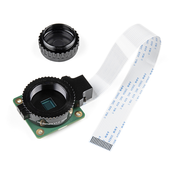

 dark grail
you would need the gerber files
eternal fox
Does anyone know if the https://www.adafruit.com/product/5752 has the same "pitch" as the https://www.adafruit.com/product/4980 when it comes to the 4 encoders vs mx compatible switches?
A tiny bit annoying that it doesnt have the same pinout as the smaller 1 encoder breakout but thats something i can ultimately live with ^^
Rotary encoders are soooo much fun! Twist em this way, then twist them that way. Unlike potentiometers, they go all the way around and often have little detents for tactile feedback. But, if ...
The only thing better than a nice mechanical key is, perhaps, FOUR mechanical keys that also can glow any color of the rainbow - and that's what the Adafruit NeoKey 1x4 QT I2C ...
Cant find any exact meassurement for the different rotary encoder spacings. I know a rotary encoder of that type has roughly the same footprint as a cherry switch.
livid sand
how do i import pcb files into fusion 360
 rustic linden
eternal fox
Does anyone know if the https://www.adafruit.com/product/5752 has the same "pitc...
rustic linden
eternal fox
Does anyone know if the https://www.adafruit.com/product/5752 has the same "pitc...
Well, both boards are exactly the same size, with the mounting holes in the same places, but the pinouts are not the same, so I'd assume the encoders and the switches are spaced out evenly on the boards, but you couldn't exactly use one or the other unless you were using Stemma QT
tough matrix
livid sand
how do i import pcb files into fusion 360
which PCB files?
Eagle? KiCad?
in general, I'd suggest exporting to STEP (KiCad and just about every other electronic design software offer that option) and then opening step file in F360
sweet cairn
So I'm implementing the PAM8302A class d mono amp in one of my project. Following adafruit's implementation of it. For capacitors, I want to go with tantalum caps because ceramic caps can introduce buzzing apparently (all this is very overkill for my project but ah wth why not at this point right?)
My question is, what should the polarity of the tantalum caps be?

The datasheet specifies that for the input caps (C4 and C5), the positive side should face the IC, but what about C3, and the filtering caps C6 and C7?

OK ig C3 is fine being ceramic then.

Nothing about the filtering caps though
 tough matrix
sweet cairn
The datasheet specifies that for the input caps (C4 and C5), the positive side s...
tough matrix
sweet cairn
The datasheet specifies that for the input caps (C4 and C5), the positive side s...
well, given that one side of these caps is connected to GND, it seems pretty clear that that side should be negative
latent jungle
sweet cairn
So I'm implementing the PAM8302A class d mono amp in one of my project. Followin...
The C_Polarized and C_Polarized_Small (I prefer the _Small variant of the passives) symbols are a better choice if you're going with tantalum, or any electrolytic. If you're using the footprints built into KiCad, it will help prefer them from getting defined backward on a PCB.
latent jungle
sweet cairn
The datasheet specifies that for the input caps (C4 and C5), the positive side s...
C6 and C7 should be C0G Ceramics (or Film.) You won't find a 220pF tantalum, anywhere.
C0G does not have piezoelectric effects.
distant raven
latent jungle
C0G does not have piezoelectric effects.
They don’t? 🤔 TIL
Ah fascinating
They don’t have ferroelectric materials
latent jungle
distant raven
They don’t? 🤔 TIL
Nope. C0G/NPO is typically made with Calcium Zirconate. Almost every other formation is made with Barium Titanate is ferroelectric.
distant raven
As I’ve said, always learning something from you 🙂
latent jungle
tldr; the barium atom doesn't fit inside of the titanate matrix, so electric and magnetic fields can move it
distant raven
Very cool bit of physics/chemistry 🙂
latent jungle
There are C0G/NPO formulations made with Barium Titante as the base material, but the dielectric is soooo thick (and/or it is doped) that the ferroelectric properties are heavily damped.
distant raven
I suppose it makes sense why you’d use C0G/NPO for things like crystal load capacitors and antenna matching networks
latent jungle
yeah. they're also ultra stable with temperature (and aging)
distant raven
I’ve used some pretty small value caps for 2nd order filters for free space optics receivers
1pF, heck even 0.5pF
It’s pretty wild we can get them that low
Digi-Key Carrie’s as low as 0.1pF which is probably as low as we can really get because you start getting to a point where the pads for the capacitor have larger capacitance
latent jungle
fun fact, some of the low-value "X5R and X7R" (100s of pF) caps are actually C0G/Calcium Zirconate. e.g. a 1206 100 pF X7R is C0G because two plates of Barium Titanate is too much cap.
latent jungle
distant raven
Digi-Key Carrie’s as low as 0.1pF which is probably as low as we can really get ...
and once you get in the sub picofarad range, the tolerance values change because 5% at that point is...well, pointless 😉
distant raven
🙂
latent jungle
Someday, I hope to remember less about capcaitors 😉
distant raven
I’m positive my wife would love if I remembered more things that weren’t electronics
latent jungle
distant raven
I’m positive my wife would love if I remembered more things that weren’t electro...
Just remember to remember the things that matter.
coarse lark
Lets say, hipothetically, that i wanted to make a development board compatible with stemma qt components/sensors. Where could i get a stemma qt smd socket? Do i need any permissions or licenses to put it in my board?
left grove
coarse lark
Lets say, hipothetically, that i wanted to make a development board compatible w...
https://learn.adafruit.com/introducing-adafruit-stemma-qt/technical-specs Hopefully that answers some questions. But I have no idea about using the "Stemma QT" (or any Adafruit) branding
(The connector is just JST SH)
coarse lark
Thx
I mainly wanted to know the connector type
I also wondered if it used a propietary connector like grove
worldly schooner
Saying it’s “StemmaQT compatible” seems to be as much as I’ve seen from non-adafruit manufacturers. If you have any plans to sell, I’d consult adafruit support and/or a relevant law professional before doing so.
coarse lark
worldly schooner
Saying it’s “StemmaQT compatible” seems to be as much as I’ve seen from non-adaf...
Im not planning on selling it, its just for my own personal use
faint rain
coarse lark
I also wondered if it used a propietary connector like grove
Grove's are compatible with 4-pin JST PH connectors. (See https://learn.adafruit.com/introducing-adafruit-stemma-qt for STEMMA (JST PH) and STEMMA QT (JST SH) details.)
coarse lark
Hmm i see
Im designing a custom ESP32-S3 dev board, and wanted to add something like a grove/stemma connector, just for fun
livid sand
does the size of via's matter or is it fine how it is
 supple pollen
For most purposes, it doesn't matter, but I tend to make them a little bigger, so the board is easier to manufacture (sometimes this translates into cheaper boards)
latent jungle
Also, larger vias can turn into (emergency) test points.
unique patio
eternal fox
Does anyone know if the https://www.adafruit.com/product/5752 has the same "pitc...
tough matrix
faint rain
Grove's are compatible with 4-pin JST PH connectors. (See <https://learn.adafrui...
not really.
You can make it kinda fit if you push hard enough, but this is not "compatible".
If Adafruit website says otherwise, they are misleading
I can make a video to illustrate it
supple pollen
I juggled how I arranged the vias on this board mostly for æsthetic reasons
 paper vale
Hello. I'm a little confuse. the nominal speed for an ebike motor is 370 RPM and the motor has a gearbox with a reduction ratio of 1:5. what is the real speed of the motor to consider when developping a control algorithm ? 370 * 5 or 370 or 370/4 RPM ?
cursive sentinel
A 1:5 ratio (assuming 1 tooth on the motor shaft per 5 teeth on the output shaft) will divide the motor rotation rate by 5.