#help-with-hw-design
1 messages · Page 15 of 1
 distant raven
I’d personally love to work for TI
They have a fab ~15 minutes down the road from me
I can see it from my 2nd story window
 woven bluff
I'd like to work for LANL (we'd neighbors ), but they rejected me after 4 month of interviews and email exchange
distant raven
Bummer. I had an offer to intern with TI but for whatever reason none of the hiring managers wanted me on their team so the offer basically expired. Apparently my GPA was too low and I wasn’t enough of an EE 🤷♂️
I did make it to the final round of interviews with them for a full time job, but I got a really good offer from where I work now so I ended up stopping the interview process
Some regrets here because that would have honestly been a cooler job
 idle python
the enable pin on the led driver lets you change the brightness via pwm, but its not at all connected to that stm32
i see the waveshare 2.8 inch screen has icn6211 and a STM32G031G8U6, and it lets you change the brightness from the pi
there are no schematics available for any waveshare screen sadly
this dfrobot screen backlight is literally controlled by a potentiometer
i looked up the stm32 chip featured on the waveshare screen, i see it has pwm output
idle python
@dry pelican i found out that the stm32 is supposed to merge the i2c for the touchscreen and the i2c configuration of the icn6211
 supple pollen
An STM32 seems like overkill for such a simple task.
idle python
supple pollen
An STM32 seems like overkill for such a simple task.
i mean im not an expert on these things so i just copied them from here
but id like to make it so i can change the brightness via i2c
 young elbow
That's a good question. The 3.3 PWM signal is coming from a Teensy. The 12v PWM will be going to a John Deere turbo charger actuator, with the duty cycle telling the actuator what position to have.
I'm not entirely sure what level of current the actuator's PCB expects, but I'm assuming 5-50ma
young elbow
Got one of these off Amazon but isn't switching the 12v input
 supple pollen
It's presumably not capable of sufficient current drive, not compatible with 3.3V logic, or a dud.
young elbow
They came in set of five; have tried different ones with same result. Wiring diagram shows 3.3v input:


 dry pelican
It may be because the micro can't supply sufficient voltage
You have a voltage drop of maybe 2-3v
Bc of the two leds in series
And then there's a resistor
The output may also not be turned on fully if the optoisolator's LED is not fully on
young elbow
Assume a good first step would be to measure voltage between input and ground pins on the chip?
dry pelican
You may want to hook up a transistor to the output of the optoisolator
In order to have more drive current
young elbow
Btw here's the chip on the board: https://datasheet.lcsc.com/lcsc/1810241112_Everlight-Elec-EL817S1-C-TU-F_C106900.pdf
 flint zodiac
good morning
I'm thinking about shortening the pads of Kicad's LQFP-64 footprint. does that shorter one in the foreground still look healthy or is it too short?

it was 1.55 mm, now it's 1.1 mm
distant raven
It probably is better to keep them longer for mechanical strength
You could shorted the part that goes behind the pin a bit, but you definitely want to make sure the pads can sufficiently hold the chip down
If it was just one pin to help you orient the index pin, sure it probably wouldn’t matter.
flint zodiac
no I'm trying to make the overall footprint smaller, not just one pad. Even shortening it to 1.3 mm would help
would look like this
 distant raven
That might be okay
young elbow
dry pelican
The output may also not be turned on fully if the optoisolator's LED is not full...
Removing the chip and wiring directly to it seems to be working the actuator. Thanks for the idea. Pretty new to circuits so still wrapping the brain around all the factors that need be accounted for
dry pelican
young elbow
Removing the chip and wiring directly to it seems to be working the actuator. Th...
Are you wiring the actuator to the microcontroller directly?
young elbow
No. Teensy -> the optocoupler chip -> actuator
dry pelican
Oh
I see
Weird that that board has an indicator led, and optoisolator and a resistor. They really shouldn't say that it works with 3.3v
young elbow
Yeah. Always a lottery with Amazon stuff
dry pelican
If the actuator were wired to the micro, you would have some  lol
lol
young elbow
I tried that initially, hoping it'd still pick up the PWM signal. No dice
dry pelican
Ooh
Wonder why the teensy wasn't
Another option would be just using a mosfet
But optoisolators give you that galvanic isolation
young elbow
So the pwm signal doesn't directly control the motor. It just tells the PCB in the actuator what position the shaft should be in
Yeah especially in automotive the isolation is nice
young elbow
Indeed
Basically I'm going to use the teensy to control a variable geometry turbocharger. So need to send PWM control signal to actuator, needs to read throttle position sensor, count tach pulse, read a couple pressure sensors, count turbo shaft RPM.
A lot to do
supple pollen
Is this like for a home power generator?
young elbow
For a truck that predates VGT turbos
supple pollen
Wow, I wouldn't hook amazon grade hardware to anything I cared about or that could run amuck, catch fire, or smash people or things.
young elbow
Oh for sure. At this point it's mostly to prove out an interface method between the teensy and actuator. If a component in the system failed worst that would happen is the turboactuator would default the vanes to the safe position which is "wide open".
supple pollen
Ah, that's not nearly as bad as a runaway diesel, which is quite a fearsome thing
young elbow
Definitely
The PCM that controls the engine and injection timing will still be there, completely separate
 hushed smelt
I'm working on a PCB to clean up the rats nest inside the mailbox. Will let me experiment with the different boards for future projects. Basically footprints for 3 separate boards in 1 one. 4 different gnd planes to an I2S amplifier. The only thing commonly connected is all the reset switches so no matter which board is connected there's 1 reset switch which runs through a 4 selector toggle switch just to ensure your not crossing ground potentials.

Everything will still be done via breadboard wires not hard traces.
Because I'll be working with audio a lot figured a basic audio out board from a variety of adafruit boards would be helpful. I2S goes out to a 3.5mm audio jack.
One thing I couldn't quite figure out is how to connect USB power + data to all of them. Will probably throw a commercial USB hub on top in there somewhere.
distant raven
hushed smelt
I'm working on a PCB to clean up the rats nest inside the mailbox. Will let me ...
Are you tying your GNDs together somehow?
If not, highly suggest using 0ohm resistors or even some large 0.1uF caps
Or simply just using one ground plane
They all have to be connected either way, you run the risk of having different ground references in each area which can cause weird voltage level issues
And also some weird transients in the analog areas which can have some not so great quality affects on your signals.
Plus you also run into the fact that signals mights not work if there is no common return
You can do individual areas on the top as long as the are all tied to a solid common ground plane on the bottom as well
hushed smelt
I don't want them to share a ground. Each section has it's own gnd
distant raven
hushed smelt
I don't want them to share a ground. Each section has it's own gnd
They have to be connected
hushed smelt
It's not like a feather doubler where they're all tied together.
hushed smelt
Each has it's own gnd plane
distant raven
That doesn’t matter
hushed smelt
Imagine 3 separate PCB's but on 1 board
distant raven
If those ground are not connected together for a shared GND reference, it won’t work
hushed smelt
They're not designed to be used together, they're meant to be used separately.
distant raven
Do you plan on hooking the Pico to the amp?
hushed smelt
That's an option yes
The gnd plane of the pico gets tied to the gnd plane of the amp with breadboard wires.
distant raven
I personally wouldn’t do that. If they are on the same board, they should share a ground. It isn’t going to hurt anything for them ti share it
hushed smelt
The qt py has 5v so i didn't want to take any chances
distant raven
As long as you don’t violate drc, you’ll be fine
hushed smelt
hmm that's not the power plane though your right
yup DRC 0 🙂
so i can swap in/out different boards for audio projects while having the amp to 3.5mm part of the board
distant raven
How about this, put a solder jumper so they can be separated but you also have the option for a much more electrically sound ground connected between the sections
hushed smelt
hmm yeah gnd plane jumping through a breadboard wire probably not the best idea
distant raven
You’re audio projects will thank you
A good ground connection can make a world of difference in audio setups
hushed smelt
ah because if i want to do gnd side switches i wanted them isolated otherwise it might trigger something on another board.
i'm just gonna try this and if it doesn't work out i'll fill the whole thing and see.
distant raven
Having ground connected isn’t going to cause anything funny
Trust me, I design lots of PCBs and have a debt paper that said I passed all my electrical engineering classes lol
hushed smelt
ok i'll give it a shot. at least could get rid of the selector switch which was an expensive part and just use a regular 6mm button switch for reset.
distant raven
hushed smelt
ok i'll give it a shot. at least could get rid of the selector switch which was...
It’ll just save some headaches down the road.
hushed smelt
what to do with the qt py 5v to gnd?
that can't share the same as the 3v3 gnd right?
dry pelican
They already have the same ground
hushed smelt
on the qt py, derp yes
dry pelican
Oh
I think you should just have the same ground plane for everything. I don’t think it matters.
But I am not an EE
distant raven
dry pelican
But I am not an EE
I’m technically not an EE, but a majority of my degree was EE
I’m a Computer Engineer/Embedded Systems Engineer
Sad part is people only read the first part of my degree field and autocomplete with “science”
hushed smelt
better?

the large capacitors are optional and experimental, if they don't help then will bridge them with 0ohm resistors
distant raven
hushed smelt
the large capacitors are optional and experimental, if they don't help then will...
Assuming the capacitors are for the speaker out?

 rustic linden
can't wait for my boards to come in
 rustic linden
especially since i can't afford anything but Global Direct Standard Freight or whatever they call it
distant raven
rustic linden
especially since i can't afford anything but Global Direct Standard Freight or w...
I could probably afford DHL but I’m cheap
hushed smelt
and that's just the wait before it actually ships
distant raven
hushed smelt
drc passed
You might want to scoot the feather connectors to the right just a bit to compensate for the slight overhang
hushed smelt
your right i didn't account for that. was going on pin square only but they are bigger
distant raven
Yeah, ever so slightly
The dimensions for the PCB itself is 2”x0.9”
Or like 23x51mm
hushed smelt

Bleeding Rainbow boards are in production now 🙂

to save more space i can put the mounting holes under the pico and feather. all the boards are going to be on female risers anyway.
will measure the boards and ensure they all fit before i send to fab, will pass by the final design here maybe tomorrow.
thank you for the advice skerr, very appreciated ❤️
hushed smelt
Got it down to 4" that will help a lot. Mailbox interior is 6.5" plenty of room for other stuff now too.
 rustic linden
What's the board? It looks like an adapter between Feather Wings, PiCowbells, and QTPy BFFs, with a headphone jack and a button
hushed smelt
That's pretty much all it is yes.
and all the button does is a universal reset no matter what board is plugged in.
Pick which board you want to use, use breadboard wires from the board to the 3W I2S amplifier, and you get a 3W audio jack out.

Hoping to clean up the rats nest inside the mailbox. The reason I added the other board footprints is because there's a minimum order of 5 so tried to figure out a way to make it generally useful for other future projects.
 silver marsh
It’s counterintuitive, but the reason the original circuit works is because the QTpy and I2S circuit ground and the analog power amp circuit ground are isolated from each other. Otherwise the neg output of the I2S amp is shorted to its ground pin. Allowing the analog amp’s ground to float along with the I2S neg output sorts out the filtered audio from the differential PWM signal. The original circuit works because the two power sources are completely isolated from each other.
hushed smelt
Are you saying tying the I2S amp to the main gnd plane was a mistake in this pcb design?
or are you talking about the way I have the mailbox currently wired?
 silver marsh
The way you have the existing working mailbox is with the I2S amp’s ground and the analog power amp’s power grounds isolated from each other, correct?
hushed smelt
yes
Here's the new setup with the 100W amp and 1x 40w speaker. The sound is excellent.
distant raven
Technically speaking, if they’re connected to the same power supply source (a plug strip for instance), they still share a common ground
silver marsh
And that’s why it works. Connecting the grounds together will be noisy and will short out the I2S amp output.
hushed smelt
The amp will get mounted inside the mailbox with the new board I'm designing. Making for an easier and cleaner install.
silver marsh
distant raven
Technically speaking, if they’re connected to the same power supply source (a pl...
Perhaps, but not confirmed in this instance.
distant raven
silver marsh
Perhaps, but not confirmed in this instance.
My if got replaced by a they for some reason lol
silver marsh
Simple to test. What happens when you jumper the two grounds together with the existing?
hushed smelt
The amp is 12V powered by a wall wart... the same as the 20W adafruit amp, also 12V wall wart. They have to be isolated or bad things will happen. 🙂
distant raven
Anyway, the negative terminal shouldn’t be shorted to ground, there should always be a filter on that path.
Like, it’s a really bad idea to short the negative I2S pin directly to ground
You’re changing the ground reference which is very very bad
hushed smelt
I can bodge wire a jump around it. That's why I made everything jumper pins so I can re-route as necessary.
distant raven
At the very least you need a capacitor to block any DC from going to ground, AC noise can be attenuated with the right setup
hushed smelt
Negative terminal isn't shorted to ground that I know of. Both positive and negative audio in/out are going directly from the amp to the audio out.
silver marsh
It’s all about converting the differential PWM output of the I2S amp to a single-ended analog input for the power amp. The power sources have to be completely isolated if an analog signal isolator transformer isn’t used.
hushed smelt
That's what the 3W I2S amp does?
hushed smelt
I'm just routing the audio out to the jack.

Pump up the volume with this 20W stereo amplifier! This slim little board has a class D amplifier onboard that can drive 2 channels of 4-8 ohm impedance speakers at 20W each. Power it with ...
This is the current 20w amp but it's getting replaced by the 100W pyle amplifier pictured above.
silver marsh
hushed smelt
That's what the 3W I2S amp does?
It creates a differential PWM signal that isn’t relative to ground; it “floats.” The analog power amp is expecting a non-differential signal relative to ground.
hushed smelt
which is why there's nothing on the board design for the 20w amp
i know i know. it's less than ideal. the pyle amp i've already tested and sounds much much better
it must have better isolation involved because it sounds crisp 👌
 silver marsh
hushed smelt
i know i know. it's less than ideal. the pyle amp i've already tested and sound...
silver marsh
hushed smelt
i know i know. it's less than ideal. the pyle amp i've already tested and sound...
It’s clever, actually, but depends on the power sources to be isolated.
distant raven
So given that, when operating properly, you should be able to connect the grounds together
hushed smelt
yes, and the 20w has i2c controls. i had to put it in analog mode, that worked much better.
distant raven
Your setup falls under the, “while it works, it’s not recommended” category lol
hushed smelt
yes
silver marsh
distant raven
So given that, when operating properly, you should be able to connect the ground...
But connecting the single-ended input to one of the differential PWM out pins would be noisy.
hushed smelt
 distant raven
silver marsh
But connecting the single-ended input to one of the differential PWM out pins wo...
distant raven
silver marsh
But connecting the single-ended input to one of the differential PWM out pins wo...
Get a preamp
hushed smelt
the 3W IS2 is my preamp 😆
distant raven
Unintended operations can lead to shorter component life, just keep that in mind.
 hushed smelt
 distant raven
Electricity is usually one area where I’d rather not risk doing things outside of the recommended application because there’s generally a good reason
Overclocking is one thing
 distant raven
Lol
hushed smelt
for science
distant raven
Anyway, be safe; report back any fires. Use a preamp next time lol
I won’t be telling my stereo junky father in law what you did because he’d drive to Florida personally 😂
hushed smelt
i don't like pwmout, i like the i2s modules. i've found them to have better quality sound.
this seemed like a reasonable compromise
distant raven
They absolutely have better quality
But there are easier and safer ways to achieve your ends 🙂
hushed smelt
and the ESP32's don't do MP3 so i had to go with the M4, thinking about switching back to the RP2040 because I cannot get it to play nice with the reed switch trigger.
distant raven
Reed switches be hard sometimes
Anyway, good luck; I wish you no random fires and no magic smoke escaping
hushed smelt
distant raven
But there are easier and safer ways to achieve your ends 🙂
Please explain? I thought this was the easiest way to do I2S. Not all boards have I2S out natively so going with a module seemed the most compatible way to drop in any board for the project... and was the right decision when I found out the ESP32 I started with couldn't do MP3.
distant raven
hushed smelt
Please explain? I thought this was the easiest way to do I2S. Not all boards ha...
Use a high quality DAC, something 12-16b
 distant raven
DACs output analog signals and audio is analog 🙂
hushed smelt
but isn't I2S a protocol that needs decoding? a dac will do that?
 worldly schooner
No, but a microcontroller can
distant raven
You can output wav data directly through a DAC
worldly schooner
With a DAC you would output the analog signal directly to an analog amplifier
distant raven
WAV is better than MP3, but you can send MP3 out a DAC as well
hushed smelt
wait.. so the mp3 through the dac wouldn't need i2s..
worldly schooner
Is the esp32 DAC good enough for audio though?
hushed smelt
yeah that's the another thing, not all boards have dacs
distant raven
I2S is generally used when DACs aren’t available
distant raven
There are also options to send your data over i2c or even SPI to an off chip DAC
hushed smelt
yes but i'm also using lora and an esp32 airlift. the mcu needs a good amount of computing power.
worldly schooner
distant raven
There are also options to send your data over i2c or even SPI to an off chip DAC
At that point, you’re using the same number of parts to accomplish the same ends. Is that easier?
hushed smelt
It's a cobble of parts no matter how you look at it depending on the features I need.
distant raven
worldly schooner
At that point, you’re using the same number of parts to accomplish the same ends...
For quality, sure
hushed smelt
Jepler just started on I2S out for the IMX maybe someday will switch to that. The lora featherwing won't be drop in but it'll eliminate the need for the airlift since the IMX has one on board.
distant raven
Yeah
hushed smelt
and if you read the datasheet the iMX has a 5 band EQ built in... looking forward to seeing someone get that working.
distant raven
Oh yeah, the iMX is a great chip
worldly schooner
Wait which imx? There’s an iMX dev board in the works?
distant raven
The one that launched 2 weeks ago
hushed smelt
the metro m7 that's already out
distant raven

Get ready for our fastest Metro ever - the NXP iMX RT1011 microcontroller powers this board with a 500 MHz ARM Cortex M7 processor. There's 4 MB of execute-in-place QSPI for firmware + ...
hushed smelt
the low amount of ram might be a concern for my project. i honestly don't know how much ram it's taking.
distant raven
I’m slowly working on an iMX8 nano carrier module to be a drop in for the CM4
hushed smelt
ohhhh
distant raven
I’ve got.. the chip and the RAM placed and I’ve started routing
But motivation is fleeting at the moment
hushed smelt
i've never heard of an imx8, datasheet?
distant raven
It’s an MPU
hushed smelt
CM4? is that the name of your watch?
hushed smelt
i saw bga and immediately closed the pdf. nope. 😛
worldly schooner
When most professional EEs hear iMX, the first thing that usually comes to mind is one of NXP’s iMX6/7/8 microprocessors haha
distant raven
But they (cm4) are super unobtainium
worldly schooner
Not a cortex M7 lol
hushed smelt
you've got to have serious skill and patience to deal with bga anything
distant raven
But I can buy iMX8 and ram so..
And PCBs
I just need to get the wires in place and then start length matching
hushed smelt
your projects are always impressive, looking forward to seeing what you do with it
you're doing tapeouts and low power circuit python watches and i'm just over here trying not to start fires.
hushed smelt
if Jepler gets the i2s working great on the rt1011 all I'd need is a LORA shield for it. That would help a lot. Maybe I could make a featherwing to shield adapter PCB hmmm.
With the amount of featherwings I have, and that are out there, that actually sounds like a great idea.
 flat vigil
I just merged in the i2s stuff
distant raven
flat vigil
I just merged in the i2s stuff
 woven bluff
what can I do to D+ and D- to make sure I can receive at least 1A?
distant raven
woven bluff
what can I do to D+ and D- to make sure I can receive at least 1A?
For like USB PD?
woven bluff
not PD, just 1A
 knotty tiger
are you going to use those lines for data at all? what kind of device will be upstream?
woven bluff
the socket is USB2.0 type-C, but if I use A-to-C cable, the upstream does not know about cc1 and cc2
no data
usb hubs, chargers, etc
distant raven
Well, power delivery will be based on upstream capabilities
knotty tiger
so chargers and hubs with type A receptacles? there's lots of protocols to choose from, and not all devices support all of them
distant raven
So if a usb hub can deliver 1A per type A port than it will deliver as much as your board draws to that limit
woven bluff
just short D+ and D-?
distant raven
Leave them floating
woven bluff
in this revision, it is floating and no problem with hubs
cc1 and cc2 is also floating
my PD power bank refuse to deliver power with C-to-C but works with A-to-C
knotty tiger
is your PD power bank USB-C? you'll need the correct pull down resistors on the CC lines, then
woven bluff
yeah, next revision will have 5k1 pull down
PD says my divergence meter is drawing 3.5W, but I'm under-driving the nixes
the next revision will have a 18650 backup, guess it will only hold 3 hours max
 broken zenith
Is there a good place to learn about the different CC resistor values of USB-C? I thought Adafruit had a Learn guide on it but I can't find it. Specifically looking for the way to get voltages other than 5V out of a USB-C port via PD. Thanks!
distant raven
broken zenith
Is there a good place to learn about the different CC resistor values of USB-C? ...
Yeah, one sec

If you’ve been following along our USB-C saga, you know that the CC wire in the USB-C cables is used for communications and polarity detection. However, what’s not as widely known is th…
broken zenith
That's just what I needed, thanks!
dry pelican
woven bluff
PD says my divergence meter is drawing 3.5W, but I'm under-driving the nixes
Maybe the boost converter is working in forced PWM mode instead of PFM or power saving mode. That would mean that it's just wasting power in order to get lower ripple.
woven bluff
dry pelican
Maybe the boost converter is working in forced PWM mode instead of PFM or power ...
max1771 only works in PFM mode
dry pelican
woven bluff
max1771 only works in PFM mode
Hmm. Is any part of the circuit getting warm?
woven bluff
just inductor
woven bluff
nixies are warm too
IN14 can be warm at 2mA, operation current is 2.5mA
there's also isolated 5V-to-12V module that feed the 12V-to-170V boost
woven bluff

adding that cap makes power consumption to go up to 10W
maybe 100p is too much for 12V-170V boost
dry pelican
Maybe you're exceeding the breakdown voltage of the cap
But that doesn't make sense either
woven bluff
that cap is rated 250V
knotty tiger
broken zenith
Is there a good place to learn about the different CC resistor values of USB-C? ...
you usually need to actually speak the digital PD protocol to get higher than 5V over USB-C. CC resistors aren't enough. there are chips that will help, though
dry pelican
FUSB302. And ST has one that has some nonvolatile memory iirc (it’s used in Sparkfun’s usbc pd board)
 fiery parcel
Hi all, I have a question about hardware design. I have a board footprint, and a couple of schematics already that I need integrated into one board. (RP2040, RFID reader, etc) is this something that's considered a difficult / expensive project?
distant raven
fiery parcel
Hi all, I have a question about hardware design. I have a board footprint, and a...
Difficulty is relative to how home grown you go with your design. Expensive will also be influenced by that as well.
fiery parcel
I need a board done relatively soon and I hardly have a budget. Was thinking of going on fiverr
distant raven
Starting out, it’s often easier to use premade modules like the Pico, and breakout boards like Adafruit modules
fiery parcel
distant raven
Starting out, it’s often easier to use premade modules like the Pico, and breako...
I've been doing this
distant raven
In terms of timeframe, it would definitely be easier and quicker to route a board where you’re just routing between modules
distant raven
If you’re looking at things being assembled by like, JLCPCB, that would save the headache of placing components yourself
There’s tons of references to follow for making a board with the RP2040, and many data sheets too have recommended schematics
fiery parcel
That's true but if I could hire someone I would
it would take a bit of load off my back
distant raven
You definitely hire someone, but consider that the cost will definitely be more.
If you’re cost and time sensitive, it would definitely be worth trying to do it yourself
what specifically are you attempting to make?
fiery parcel
It's the PCB for the toy im working on
right now, its got a Feather RP2040, an RFID Reader, and an audio amp for components
distant raven
Okay
dry pelican
Sparkfun has their A La Carte service. You put down a few standardized modules, and they'll design and build a board for you
dry pelican
I'm thinking of making a tDCS device. I've read into it and it seems that 4-5mA is the maximum safe current output. (Treatment is usually at like 2mA) I want to design the current control and monitoring circuit (as well as the boost circuit (to get enough voltage for 4-5mA max) in such a way that there will never be more than 4 or 5mA (depending on where I set the final current limit) going through the output terminals. My current idea is to have a current limited boost converter powering everything. The boosted voltage goes into the op amp constant current regulator (which is set by the amplified voltage from an I2C DAC) and the current going to the tDCS connectors is sensed by a precise INA237. The INA237 can read the current and voltage back as well as have an alert interrupt that can be configured to trigger when current goes over a certain limit. When the INT line gets pulled low, the NPN transistor that was turned on by the enable power GPIO (ENout) gets turned off, which turns off the output.

Is this pretty much as safe as possible?
supple pollen
Not yet, but you're getting there.
dry pelican
supple pollen
Not yet, but you're getting there.
How could I improve the safety of the device?
supple pollen
Limit the power supply voltage, have a minimum impedance on the output, use galvanic isolation, etc.
dry pelican
Do you mean galvanic isolation from mains for the whole circuit or just isolation for the tDCS CC circuit from the rest of the circuit?
 river glen
Hey so I am working on a circuit that has a voltage regulator with reverse current protection. I want to add a switch that will turn off the load (VCC) when the temperature gets too hot


Would the best bet be to just add a second mosfet? Is it normal to have two mosfets in a row? It's a little weird because signal voltage is 0-3.3v with active low
 dry pelican
You might be able to integrate the alarm signal with some smart circuit design or use another p channel with an npn inverter after the reverse current protection p channel fet.
That reverse current protection circuit looks kinda weird tho
The mosfet's body diode would allow current to flow in reverse even if the fet is switched off
And that schottky diode connected to the gate would turn the mosfet on when there is reverse current
river glen

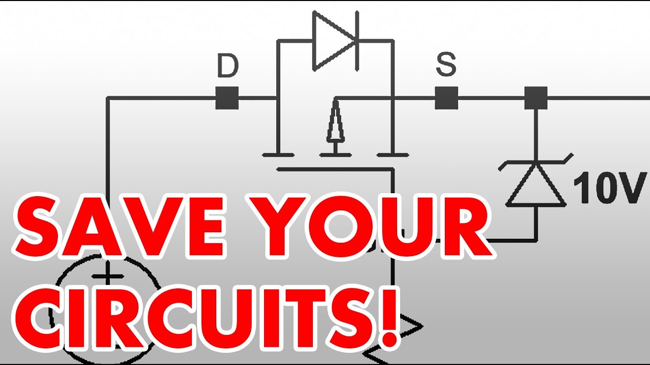
How to use diodes, schottky diodes and P-FETs to protect your circuits from reversed voltage/power connections.
Website: http://www.afrotechmods.com/
I tried to design it based on this
I should appologize, VCC is the "load" in this circuit
dry pelican
Your p channel is backwards then
dry pelican
river glen
I should appologize, VCC is the "load" in this circuit
Ahhhhhhh
That makes a lot more sense now
river glen
So it wouldnt be a big deal if I added another mosfet probably, just cost wise
since this circuit sees about .35a at full load
I put this into a simulator and played around with voltages, I couldnt get it to shut off when voltage was positive
Would I just put an N channel mosfet after that P channel and use a transistor to drive that in such a way that the low turns it on?
dry pelican
You want to make sure your voltage references are good (n channels do low side, p channels do high side. If you're trying to use N channels for high side or p channels for low side you need a bootstrap circuit). A P channel before the reverse voltage protector that has its body diode reverse biased would do the trick
And add an NPN transistor and resistor for an inverter
Why would the circuit get too hot though?
Buck converters are pretty efficient
Unless you're powering a heater or something that has enough power loss/consumption to get too hot
What is VCC's voltage?
river glen
well
it's basically insulated
VIN is 12-24v max
I am making LED panels with acoustic foam as the diffuser, so it's effectively insulated
it should be fine but I want the safety margin
broken zenith
Would a chip like the ATTINY841 require lots of passive components (capacitors, xtal, etc.)? I can't find an application diagram in the datasheet that I'm looking at, and I don't know how to read the electrical characteristics yet.
https://www.digikey.com/en/products/detail/microchip-technology/ATTINY841-MMHR/4437425
Please ping me if you have any thoughts. Thanks!
river glen
dry pelican
You want to make sure your voltage references are good (n channels do low side, ...
got it thanks
distant raven
broken zenith
Would a chip like the ATTINY841 require lots of passive components (capacitors, ...

From sparkfun via a google search
That hooks up to an NRF24L01
So just ignore the NRF part
broken zenith
Ok, thanks so much! I really appreciate all of your help recently.
 broken zenith
That's optional right? Trying to keep this design (e-fidget) simple
distant raven
Yeah
broken zenith
Ok, thanks
supple pollen
dry pelican
Do you mean galvanic isolation from mains for the whole circuit or just isolatio...
Either is fine, as long as anything connected to the body is completely isolated from mains.
dry pelican
supple pollen
Either is fine, as long as anything connected to the body is completely isolated...
It'll likely be powered by a battery. And I will add a zener diode on the output to prevent overvoltages as well as a resistor to limit the output current if everything else in the circuit fails
 brittle isle
I need to use a transistor to convert a gpio signal to a 3.3v line, I have an assortment of transistors, and now idea how to pick the right one for the job
This is the assortment I have. Which tranistor should I use?
 distant raven
brittle isle
This is the assortment I have. Which tranistor should I use?
distant raven
brittle isle
This is the assortment I have. Which tranistor should I use?
So these are BJT which are not well suited for voltage level translation
You will want a mosfet, something like a bss138
Or a proper bi directional translator

Because the Arduino (and Basic Stamp) are 5V devices, and most modern sensors, displays, flashcards, and modes are 3.3V-only, many makers find that they need to perform level ...
This this
brittle isle
There's 4 on there?
distant raven
Yeah, how many do you need?
brittle isle
all im trying to do is power some LEDs on my address and data lines so I can read the byte value easy
so 16 total
8 for data 8 for address
distant raven

Because the Arduino (and Basic Stamp) are 5V devices, and most modern sensors, displays, flashcards, and modes are 3.3V-only, many makers find that they need to perform level ...
brittle isle

DollaTek 8 Channel Logic Level Bi-Directional Converter Module TXS0108E TXB0108
trying to order on amazon because this piece is like all I need
distant raven
Slightly different but should work I guess
brittle isle
ordered
in the meme time, I guess I don't necessarily NEED the LEDs to work on this
distant raven
In the meme time.. I’m stealing that
brittle isle
lol
supple pollen
brittle isle
I need to use a transistor to convert a gpio signal to a 3.3v line, I have an as...
If it's an output circuit, you don't even need a transistor, you can build a voltage divider out of two resistors.
 rigid plume
Can anyone check if I've done my schematic right :), I'm making a SIM800C where I want to make calls, hence the headphone jack, aswell as doing other tasks. 2G is still in my country so that is fine.


 supple pollen
That thing will not be happy running from USB power. What sort of battery do you have in mind? L4 will need to be beefy - did you work out the inductor selection equations? I'm interested in the double ESD protection for the SIM card.
rigid plume
supple pollen
That thing will not be happy running from USB power. What sort of battery do yo...
Well I'm using battery power mainly, just usb c for programming the esp32 s3, it has an IP5306-I2C for that
The inductor is this https://www.lcsc.com/product-detail/Inductors-SMD_PSA-Prosperity-Dielectrics-MCS0530-4R7MN2_C2836880.html
MCS0530-4R7MN2 PSA(Prosperity Dielectrics) US$0.0798 - 3.5A 4.7uH ±20% 5A 50mΩ SMD,5.2x5.4mm Inductors (SMD) ROHS datasheet, price, inventory C2836880
It looks fine and it is probably enough I hope
Also the ESD protection is what I see some people suggest since the SIM800C is sensitive
supple pollen
I've always powered the SIM chips directly from LiPo cells, but that converter seems like it should work
 rigid plume
That looks nice
I think using the IP5306-I2C is great for these features: Increased Flexibility: The I2C interface allows the IP5306-I2C to be controlled and configured by a microcontroller, offering greater flexibility in managing power and charging functions.
Reduced Component Count: The I2C interface eliminates the need for additional external components, such as MOSFETs or resistors, that would be required to implement power management and charging functionality in the non-I2C version of the IP5306. This can help reduce component count and simplify PCB layout.
Real-time Monitoring: The I2C interface allows real-time monitoring of various parameters, such as battery voltage, charging current, and temperature, which can be useful for optimizing power management and detecting potential issues.
Improved Safety: The IP5306-I2C includes safety features such as overvoltage and overcurrent protection, which can help protect the device and the battery from damage due to unexpected voltage or current spikes.
Ease of Integration: The IP5306-I2C is designed for easy integration into existing designs and can be used with a variety of battery chemistries and charging configurations.
supple pollen
I take it the "LED" pins do double duty as I2C pins?
rigid plume
Yeap
supple pollen
Note that you may not need those level converters
rigid plume
I think I will just keep them there just incase
Other than that do you think my schematic is fine? Thanks
supple pollen
Nothing else jumps out at me
The aggressive power decoupling seems like a good idea
rigid plume
Yep it would help alot, thanks for your help
supple pollen
Here's a pic of a (slightly later revision) board with its various antennæ and peripherals in place
 rigid plume
Looks nice, what is the GPS chip?
supple pollen
The SIM808 does both GSM and GPS, which was handy
Although I had to add an outboard network to use an active patch antenna, as the SIM808 only has support for a passive antenna.
rigid plume
I see
The SIM808 looks great with added GPS functionality, the SIM800C i'm using is like a basic compact version of it
supple pollen
Yup
rigid plume
What's the MCU on your board?
supple pollen
Texas Instruments MSP430FR5969. I wanted my board to be able to carry information through total power failure, and the FR series has FRAM that can be used as non-volatile SRAM.
It's also the lowest power consumption available in the MSP430 line
rigid plume
Never heard of those MCU's but they look interesting what was your board for?
supple pollen
It was for tracking high-value merchandise, and could communicate via WiFi, Bluetooth, and GSM. There was also provision for tamper detection and some other goodies.
"Homer" for the ability to get things home again
rigid plume
Wow, sounds great
supple pollen
The first version, I got the pin numbering wrong for one side of the SIM808 footprint, hence the bodge wires
 rigid plume
I like the board layout it looks nice
supple pollen
Thanks!
rigid plume
Why did you put the SIM chip so close to micro b port?
supple pollen
Trying to get the cellular signal pushed as close to the edge of the board as possible, so as not to interfere with the other circuitry. Also the micro B port was to talk to the SIM module anyway, so it made for short USB data lines.
rigid plume
Oh sure
Also, what chip would you recommend for 4G?, since 2G is going out soon in like 5 years for the UK
supple pollen
I'm looking at the SIM7600 series currently, there are variants for different parts of the world. I think some of the other vendors (Quectel? uBlox?) have offerings as well.
They also include satellite positioning support as a bonus
rigid plume
I see, what do you think about the A7670- I think it supports 4G
rigid plume
supple pollen
They also include satellite positioning support as a bonus
Thanks will research that chip
supple pollen
I hadn't looked at the A7670 series, so I'm not sure what the differences are.
That's a nice little breakout board
rigid plume
Thanks for your help
rigid plume
supple pollen
I hadn't looked at the A7670 series, so I'm not sure what the differences are.
Hi, I have a question for the ADC from the SIM800C, can I leave it floating like this and connect it to a header just incase it is needed later
 supple pollen
Yeah, should be fine. I like to allow for future expansion like that.
rigid plume
That's great thanks
rigid plume
supple pollen
Yeah, should be fine. I like to allow for future expansion like that.
Hi, sorry for all the questions

I want to use another switch which is labelled 2 in this image, am I doing the circuit right? Thanks
The first one was the original circuit that works
 unreal flax
rigid plume
I want to use another switch which is labelled 2 in this image, am I doing the c...
unreal flax
rigid plume
I want to use another switch which is labelled 2 in this image, am I doing the c...
Unfortunately, no. You've got the ESP_EN pin directly connected to ground there, for example. You'll want to follow the original schematic more closely but just swap out the button portion of it for the new part.
rigid plume
unreal flax
Unfortunately, no. You've got the ESP_EN pin directly connected to ground there,...
Something like this?

Thanks
unreal flax
rigid plume
Something like this?
Yep! Nicely done, that looks good. 👍
rigid plume
unreal flax
Yep! Nicely done, that looks good. 👍
Thanks 🙂
 rich sorrel
Hey folks, got a mystery LCD display, looking for a datasheet or some way to control it. It's from the first ZipIt wireless messenger, 320x240x4. 24 pin FPC, although only 18 pins are populated. The FPC is branded Wintek, and their display models have similar numbers, but I can't find this one.
Likely STN, given the specs of the ZipIt's cpu/lcd controller. The ZipIt is dead, so I can't probe it while it's running.
I tried diving into the kernel drivers on https://elinux.org/ZipIt_Tech_Details#Source_Code but I'm not knowledgeable enough to figure out what parts of the kernel are doing the displaying, versus other display drivers that are just part of the kernel.
 rigid plume
Hi, I have another question with my schematic design I was wondering if the voltage outputs such as +5v and VBAT are correct, because I think they're wrong. I'm using the IP5306-I2C, and I don't know if the VBUS has to go into it first then exit to the regulator. Thanks
 rigid plume
Hi @unreal flax if your able to help, sorry for the ping.
supple pollen
rigid plume
Hi, I have another question with my schematic design I was wondering if the volt...
It looks like the IP5306 either bridges VUSB to +5V, or generates +5V from VBAT. If so, you don't need the diode and MOSFET before the 3V3 regulator, just run the +5V output from the IP5306 to it.
unreal flax
The IP5306 datasheet uses a 0.5-ohm resistor between VBAT and the BAT pin, though I'm not quite sure why, but it is a difference from your schematic.
rigid plume
I don't think the resistor is necessary, I'm not quite sure
rigid plume
supple pollen
It looks like the IP5306 either bridges VUSB to +5V, or generates +5V from VBAT....
Would this be fine? Thanks
 supple pollen
Yeah, looks like there's 22µF from the cell to ground, and the 0.5Ω resistor in series with a second 22µF capacitor to ground, presumably forming a decoupling network/low-pass filter for the battery voltage to the battery voltage sense pin. Without it, the voltage variations into the coil to the switching pin could confuse the chip's battery voltage sensing circuitry.
rigid plume
Hmm, I'll add that just incase
supple pollen
Note: I'm unclear on what 3V3_EN and ES_3V3 are for.
rigid plume
supple pollen
Note: I'm unclear on what 3V3_EN and ES_3V3 are for.
They're just generic pins ES_3V3 is for monitoring and 3V3_EN isn't connected to anything except an header
supple pollen
Also note: the 3 22µF capacitors on the 5V line coming from the IP5306, along with the 10µF and 47µF capacitors on the input to the 3V3 regulator, are all effectively in parallel.
Also also note: now VSYS is synonymous with +5V, so you probably don't need two net names.
rigid plume
supple pollen
Also note: the 3 22µF capacitors on the 5V line coming from the IP5306, along w...
Is this bad, I can't tell. 😄
supple pollen
It's not necessarily bad, just seems an odd selection of parallel values
rigid plume
I see, also are you sure an 0.5ohm resistor is needed, it seems very odd to add one, and an odd value.
I can't tell from the datasheet as it doesn't list resistor values
supple pollen
While I suspect the value isn't critical, you probably do want some decoupling between the electrically noisy signal at the battery/inductor junction and the voltage sensing node.
 tulip topaz
rigid plume
I see, also are you sure an 0.5ohm resistor is needed, it seems very odd to add ...
tulip topaz
rigid plume
I see, also are you sure an 0.5ohm resistor is needed, it seems very odd to add ...
I would assume It’s needed.
woven bluff
any recommendation of fixed frequency MSPS controller to replace max1771?
supple pollen
woven bluff
any recommendation of fixed frequency MSPS controller to replace max1771?
You have asked this a few times now, in different forms. What specifically are you trying to accomplish? Which features of the 1771 are important to you? Which features don't matter? Are you looking for a particular frequency, mode, or configuration? Do you need a particular kind of package? Are you flexible on external/internal switching?
 opaque comet
Hi everyone! I'm hoping someone can help me. I'm using a TI SN74HC4852DR to select UART pins on a pico. I have the A/B connected to a DIP switch where one end of the switches are connected to 5V and the ON ends are connected to the A/B pins of the SN74HC4852DR each with their own 10K pull down resistor. I don't believe the pulldown resistors are doing what I expect them to do (pull the A/B pins low when the DIP is switched off). When I set both switches to ON the correct pins are output on the SN74HC4852DR so I know that's working at least. Any suggestions on where to start troubleshooting?
supple pollen
I'd measure the voltage on the A/B pins with the switches on and off
supple pollen
It sounds like your switching arrangement is doing what you want it to, then, so the problem reduces to figuring out why the chip isn't acting as expected
opaque comet
so these things are meant for logic output from like an MCU... am I wrong in thinking I can just use a pulldown to GND to "simulate" low from an MCU?
is there something in the datasheet I should be looking for to tell me if I have the proper pulldown resistor value?
supple pollen
In general you're right, but some older logic families (like TTL) need a particularly strong pulldown to get a reliable logic low. However the HC series is high impedance and should work fine that way.
Since the input measures 0V, your pulldown is working correctly.
I'm guessing the real problem is something like an unconnected input. Presumably you're routing the two signals to be switched to 1Y0 (pin 12) and 1Y1 (pin 14), and taking the switched signal from 1Z (pin 13), you're switching S0 (pin 10) and grounding S1 (pin 9) and /E (pin 6)?
opaque comet
so by default, S0 and S1 (9/10) are low (from my pulldown), which should enable 1Y0 and 2Y0.
when I set both switches to ON S0/S1 get 5V and 1Y3 and 2Y3 are enabled (this works)
and yes, I am setting EN (pin6) low to GND
I have a jumper to GND connected to pin 6
also with a 10k pulldown resistor
supple pollen
Weird. That leaves things like mismatched ground references, out of range voltages, a problem with the chip itself, or something I haven't thought of.
opaque comet
I built a PCB so all the GNDs are connected
the voltages does raise a question tho
does the SN74HC4852DR VCC need to match the logic voltage?
I routed 5V from VBUS on the picoprobe to VCC of the SN74HC4852DR and the uart is presumably using 3.3V
should I have used the 3.3V from the pico to VCC on SN74HC4852DR
supple pollen
That should be fine, it's an analog switch, so should happily pass voltages between ground and its supply voltage (0-5V). So 0-3.3V should be fine (the other way around could cause problems, but that's not your situation)
You're switching between different pins on the same Pico?
 dapper niche
anyone familiar with particle argons i need help trying to put it together and then try get the LED to blink morse code
opaque comet
so the board basically connects a picoprobe to a target pico... and I am using the common pins of the SN74HC4852DR to the picoprobe UART, and want to be able to switch to different UART pairs of the target pico
so yes, I'm trying to switch between different pins of the same target pico
supple pollen
Did you perhaps route RX to RX instead of RX to TX on one port?
opaque comet
I checked that... I'm not
supple pollen
Then we're down to the last 2...
opaque comet
I've got all the TX and RX pins on the same side of the SN74HC4852DR and routed them all the same according to the pico pinout
supple pollen
Or the target Pico isn't routing the signals to the pins you have connected
opaque comet
to clarify 1Y = TX and 2Y = RX... so since XY3 works... I don't think it's connected wrong
I manually defined them with stdio_uart_init_full(uart0, PICO_DEFAULT_UART_BAUD_RATE, 0, 1); to be sure I was
supple pollen
So that's D0 and D1?
opaque comet
and I explicitly uart_puts(uart0, "blah");
opaque comet
supple pollen
So that's D0 and D1?
not sure what D refers to... those pins are connected to 1Y0 and 2Y0
but on the pico.. those are GP0 and GP1
supple pollen
You said stdio_uart_init_full(uart0, PICO_DEFAULT_UART_BAUD_RATE, 0, 1); does that mean that you're routing RX and TX to the D0 and D1 pins?
opaque comet
yes, that's correct
supple pollen
Ah, GP0 and GP1. Same notion, different naming convention.
Is that on the probe or the target?
supple pollen
So what's the other UART on the target routed to?
supple pollen
Have you validated that works as desired?
opaque comet
uart1 (GP8/GP9), uart0 (GP12/GP13), uart0 (GP16/GP17)
and yes, I've used all those pins as UART and they work as expected when directly connected
supple pollen
Then again, we're down to the last two
opaque comet
could it be the chip tho if it works when both pins are high?
supple pollen
Yeah, chips can fail in a myriad of ways
opaque comet
okay.. I'll keep playing around and see what I can find out. Thanks for the advice.
opaque comet
@supple pollen update. Chip is fine. Issue with plating on 2 multilayer pads on the pcb making 2 of the combos not working.
Bad footprint 🤦🏻♂️. I should have known better than to trust a community uploaded footprint for the Pico without verifying it.
supple pollen
Ouch. That was a real headscratcher.
But thanks for sharing what you discovered, I was curious!
opaque comet
Yea, I really wanted to validate that the dip switch would work for the logic which you answered.
supple pollen
Yeah, that approach is solid.
woven bluff
supple pollen
You have asked this a few times now, in different forms. What specifically are ...
I have hot inductor issue (not saturated). I need alternative 170V supply for my nixies. the 1771 is nice because of low external component count, but switching frequency too low thus require huge inductor, also too sensitive to feedback node noise. non-FN or BGA package. internal switching not possible with this high voltage
supple pollen
I've stopped rolling my own nixie supplies, opting for the Tayloredge ones, but my previous reply about the MC34063 and related chips should point you in the right direction.
Some useful reading here https://hackaday.io/project/160535-nixie-tube-high-voltage-power-supply
hushed smelt
170V? Good lord.
dry pelican
woven bluff
I have hot inductor issue (not saturated). I need alternative 170V supply for my...
Since you don’t need high current capability, maybe a BJT instead of a mosfet might be good at high switching frequencies. Higher voltage fets usually have higher gate capacitances, which means they take more energy to switch at higher frequencies. But you still need to find a high frequency boost converter
That supports an external FET/bjt
supple pollen
170V isn't that hard, but it is a large boost ratio from 12V and even more so from 5V, so a pure inductor flyback converter is going to have an unattractive duty cycle. Transformer based ones make it easier.
 dry pelican
Agreed. Flyback converter prolly makes sense at that point
555 timer might even be able to provide the signal
But voltage would not be very regulated
supple pollen
It's not hard to build a 555 based boost converter with voltage regulation. They're not particularly efficient, but they're easier to get working than the more complex MAX1771 and MC34063 circuits.
woven bluff
WE-FLEX seem to be able to reach 1:5 ratio but they are quite bulky
as for controller, most of them are multi-topology and there is nothing simpler than max1771
if I switch to flyback I might as well get the isolation done. In my current design the isolation is provided by commercial 5-to-12V module
dry pelican
I think the UCC3808 is built for fly back driving or something
woven bluff
it's too expensive too make a chip that only support one topology
for flyback with isolation, the feedback is problem, unless there's primary side sensing
supple pollen
The usual approach is an optocoupler to route the feedback across the isolation barrier
 stoic birch
anyone know why i am getting these reads direct from adc? they are on a analog stick with x and y axis. i've checked for bodges and can't find any. y chanel seems consistent but x has what appears to be random reads
y axis is fine in print values, x seems so random to me
it holds it's mid value but the moment it goes + or - it does the cycle down to 0 and doesn't hold any area
also the mini joycon like buttons from adafruit dont click after pressing it like 5 times but that's a build issue
i also had a faulty one before
guess i'll just try another stick
another bad stick
this one works flawless and the push action currently works
we're gaming
now to superglue it in place
dry pelican
supple pollen
The usual approach is an optocoupler to route the feedback across the isolation ...
👆
That's the approach most switching power adapters use to isolate input and output. I wonder if you could abuse one of those smps ics as a step up flyback instead of a step down flyback.
 opal rapids
what's the thing holding the resistance wire called

not the whole enclosure, just the little ceramic thing the wire sits inside of
distant raven
opal rapids
what's the thing holding the resistance wire called
I’d guess something along the lines of a ceramic insulator
 regal lodge
if I need a crap ton of voltages in a design, what's the best/most efficient way to do that? (Input voltage will be 5-20V; output should be 1.2V, 3.3V, 5V, and 12V -- I plan to have the 12V disabled if the supplied voltage is under 15V, but the other voltages need to work even if the supply is 5V)
distant raven
regal lodge
if I need a crap ton of voltages in a design, what's the best/most efficient way...
There are a handful of chips that will spit out a few voltages
regal lodge
yeah I looked into that but they are like $30+ lol
one thing I'm really not sure about is 5V
most/all of the regulators I looked at need higher than 5V to make 5V
how do I get a 5V regulator that operates at 5-20V
I looked at buck-boost ones but they seem to also not like getting exactly their output
distant raven
buck boost will be your best bet for 5V, and 12V
regal lodge
I'm fine with 12V not being there when supply is <15V
distant raven
there are lots of good 1.2V and 3.3V regulators that take a wide input.
regal lodge
yeah 1.2V and 3.3V stand alone regulators seem pretty straightforward
but 5V has me stumped
distant raven
I would suggest using a beefy 5V buck boost and driving the 1.2 and 3.3 regulators
and using a boost to get 12V
or just a 5V buck that takes 5V-24V
or more if you want.
use this to get 5V and up to 5A (not sure what kind of loads your running)
this will give you 25W of power
distant raven
do you know your power budget?
regal lodge
1.2V is for the FPGA which is very light, like 30mA
the most power hungry thing would be the SoC, let me check its datasheet quick
1A peak under a worst case full-load max-temp situation

that's on the 3.3V
it's a bit more complicated than the atmega2560s I normally work with 😅
 distant raven
regal lodge
it's a bit more complicated than the atmega2560s I normally work with 😅
distant raven
regal lodge
it's a bit more complicated than the atmega2560s I normally work with 😅
Okay, so I would personally plan for at least 1.5A draw
Maybe 2A depending on what you’re doing with the 12V supply
dry pelican
I think that most 5v buck converters will just spit out close to 5v (5v minus diode drop) with an input of 5v. A datasheet for a TI simple switcher buck said that it will output at least 95% of vin iirc
distant raven
yeah
I think what i'd do.. buck/boost to 12V, buck/boost 5V, and then tie in 3.3V and 1.2V off the 5V supply
either LDO or buck
dry pelican
Or you could do some goofy thing like hook up the 5v buck to the 12v buck boost.
Not that goofy tho
distant raven
you could for sure
dry pelican
Depending on power needed
If you don't need much out of 12v or 5v, it would work. But 5v is probably the main rail
distant raven
they said they would like to omit 12V if voltage is less than 15V so having 12V separate would meet that requirement
dry pelican
There is an interesting PMIC in the M5stack core2
But it's more for battery powered and lower current
distant raven
yeah
regal lodge
yeah, 12V is a niche use, most people won't need it
I'm making a supply based on USB-PD, the idea being if they plug in a 15-20V capable PD supply they get 12V
otherwise they do not
on another note, how's this look...
 dry pelican
regal lodge
I'm making a supply based on USB-PD, the idea being if they plug in a 15-20V cap...
dry pelican
regal lodge
I'm making a supply based on USB-PD, the idea being if they plug in a 15-20V cap...
Why the SoC and FPGA then? Or is that a different thing?
dry pelican
You shouldn’t need a FPGA and SoC for a USBC PD powered supply unless it’s doing something more
dry pelican
Makes sense
regal lodge
it's a thing that interfaces with other things
rarely some of those things want 12V
I figured these days most geeky type people have a USB PD supply kicking around so if they need 12V for a once off they can borrow their phone/laptop/tablet/etc charger for a few minutes and save having to get some random 12V wall wart they'll use once
regal lodge
regal lodge
on another note, how's this look...
hopefully I wired this right, tried to follow the datasheet but idk if I did it right XD

for the same project btw lol
here's the datasheet for that chip, https://www.ti.com/lit/ds/symlink/sn74gtl2003.pdf
 paper vale
Hello. Please do the Quectel BC660K-GL NB-IoT module needs anything special to work on all GSM/LTE bands ? because since at least 3 days it doesn't able to attach on any of my operators. I wonder if a problem is with the antenna or the NB-IoT coverage
dry pelican
regal lodge
hopefully I wired this right, tried to follow the datasheet but idk if I did it ...
Sref should not have a 200k resistor
 young elbow
Anyone decently versed in ATX psus? I'm using the ~40 amp 12v rail to power an actuator that I've been controlling via an arduino. When the actuator does a big change from one extreme to the other, the ATX shuts itself down for a few minutes
I've measured the actuator drawing 5 amps... Maybe it could draw 8 or 10 at most. I don't really understand why a sudden momentary draw that's well within it's amperage capability would cause a PSU to go in to protection
 fluid lark
Ok, so, Ill ask here cause I'm so PCB inept, how hard would making a PCB for this with a keypad macro matrix work? And how would I do it?

 cinder anchor
fluid lark
Ok, so, Ill ask here cause I'm so PCB inept, how hard would making a PCB for thi...
cinder anchor
fluid lark
Ok, so, Ill ask here cause I'm so PCB inept, how hard would making a PCB for thi...
Hey Velo, take a look at this Learn article: https://learn.adafruit.com/deluxe-4x4-neopixel-neokey-keypad

Adafruit Learning System
Build a highly posh keypad with aluminum enclosure
cinder anchor
fluid lark
Ok, so, Ill ask here cause I'm so PCB inept, how hard would making a PCB for thi...
Making your own PCB shouldn't be too hard if you follow the schematics that already exist for the RP2040 MacroPad or similar. I recommend KiCad as it is free.
Unless you really want to make a PCB, you can use the NeoKey hot-swappable Ortho to build many different configs of macropads and keyboards: https://www.adafruit.com/product/5157
For folks who want ready-to-go keeb action, we've got the lovely Adafruit Macropad with a 3x4 grid of MX+NeoPixel key switches - but for those who like to forge their own path, we now ...
fluid lark
Thanks for these!
cinder anchor
Yup yup! I am going that route myself before I jump into making a PCB for the thing... Those snap-aparts are glorious for prototyping a macro pad.
rustic linden
cinder anchor
Unless you really want to make a PCB, you can use the NeoKey hot-swappable Ortho...
Forgot about this product, but this is a great suggestion, as it takes all the difficulty out of making a key matrix
woven bluff
supple pollen
The usual approach is an optocoupler to route the feedback across the isolation ...

this has primary side sensing and 42V switch
 balmy tide
@regal lodge if your FPGA has development board see if they have multi rail power ics. Usually someone else already done homework for you.
rustic linden
woven bluff
macropad just connect keys directly to GPIOs
yeah, it's why i used that approach for mine
 digital moat
forgive me if this is the wrong forum. We currently use the two of the TLC5947 chips and the https://github.com/adafruit/Adafruit_TLC5947 library to drive 16 rgbw leds. I was looking at newer chips like the TLC5955 https://www.ti.com/product/TLC5955 so we would only need one control chip instead of two. While there is an arduino library for it https://github.com/zackphillips/TLC5955 there is no circuitpython library. I see that some work was done for a similar chip TLC5957 https://www.ti.com/product/TLC5957 but the library was never completed https://github.com/s-light/slight_CircuitPython_TLC5957. May I please ask where I should turn for help only to understand whether there may be a way forward to result in a CP library for the TLC5955 somehow?

GitHub
Adafruit's Arduino driver for the TLC5947. Contribute to adafruit/Adafruit_TLC5947 development by creating an account on GitHub.
TI’s TLC5955 is a 48ch, 16bit PWM LED driver with dot-correction, brightness control, open/Short Detection. Find parameters, ordering and quality information

GitHub
Arduino library for the TI TLC5955 LED controller. Contribute to zackphillips/TLC5955 development by creating an account on GitHub.
TI’s TLC5957 is a 48-channel, 16bit ES-PWM LED driver w/ pre-charge FET, LED open Detection and caterpillar cancelling. Find parameters, ordering and quality information
supple pollen
woven bluff
Yes, primary side sensing or feedback winding sensing are the other approaches.
dry pelican
You can make your own cp library
stoic birch
switch like joycons - garbage - first the push function just vanishes after like 10 presses and it seems to short on one or both axis'
stoic birch
replaced with more industrial. i wouldn't recommend those switch like joycons, all the ones i had broke as soon as the push button gave up which was very fast
supple pollen
We had controllers we were fielding for the military and they tended to fail quickly. We upgraded to "industrial" but those failed quickly too. Then we upgraded to very expensive "mil spec", which also failed quickly. Then I suggested we go to "arcade spec", which isn't too expensive, and is designed to keep working in a bar, with beer, cigarette ash, and abuse from drunken people taken into account. That stuff lasted quite well.
stoic birch
well these joycons simply don't work. u get one good read the voltage just goes haywire
at least the other one seems to be consistent
supple pollen
The "mil spec" ones had hardened shafts to avoid bending from pressure. The arcade ones had ordinary plastic shafts, but they were mounted in spring loaded bearings, and there was a solid bumper underneath to limit the total motion. All cheap molded plastic, but amazingly durable.
stoic birch
yeh the other stick is crude looking but very solid
supple pollen
Yeah, joycons are famously designed to just get replaced.
stoic birch
they're utter crap. i wasted so much time on this print thinking that nahhh it was just one i returned, 4 sticks later same situation
yep crap
oh well gives me a chance for more iteration


 zinc basalt
hey guys, I'm interested in making some very basic PCB designs (i.e. no more complicated than a minimal design RP2040, mostly keyboard PCBs with no RGB). I was wondering if it makes sense to use KiCAD for something like this, or if Fritzing's PCB design tools would make sense for simple projects? I was looking at JP's guide and that prompted the question: https://learn.adafruit.com/diy-pico-mechanical-keyboard-with-fritzing-circuitpython/make-a-custom-pcb-with-fritzing

Adafruit Learning System
Build your own custom mech keyboard that runs CircuitPython on the Raspberry Pi Pico RP2040
 low anchor
Personally I've enjoyed using kicad a lot and I found fritzing's system to be frustrating. But you can use either, it's just a matter of preference
stoic birch
could someone recommend heatshrink size for electronic wire?
i was looking at 3mm which is 2:1 shrink size, i'm assuming this will shrink to half the size and 1.5mm in total. maybe this is the one since my electronic wire is about 1.5mm wide
zinc basalt
low anchor
Personally I've enjoyed using kicad a lot and I found fritzing's system to be fr...
Would you say the learning curve is different between the two?
and, does Adafruit have any guides written for navigating KiCAD? JP's Fritzing guide is very good for teaching.
dry pelican
There are some videos on the digikey YouTube channel about using kicad (it’s an older version, but the main controls have probably not changed much, so it’s still good)
stoic birch
there's an element14 presents kicad run through and a few others on YT
 supple pollen
The graphic on the Pico footprint oddly reminds me of the "companion" creature in the ST:TOS ep "Metamorphosis".

 vestal crystal
Sorry if this is the wrong place to ask, but does anyone know where to get started on slapping a humidity sensor into a MagTag? I looked around for a bit and I think if I got a AHT20 sensor and a Stemma QT to QT cable that'd work? But also those cables seem to be out so wondering if there's alternatives and also if I'm looking at the wrong things.
(this sensor https://www.adafruit.com/product/4566)
The more I'm looking at this the more I think I do indeed need those out of stock cables, hrm.
dry pelican
Sparkfun may have them
Qwiic is the same standard
and there are now amazon knockoff qwiic/stemma QT cables
hushed smelt
@vestal crystal #help-with-circuitpython is the best place for help for the Magtag
 unique patio
vestal crystal
The more I'm looking at this the more I think I do indeed need those out of stoc...
unique patio
vestal crystal
The more I'm looking at this the more I think I do indeed need those out of stoc...
DigiKey has some cables in stock: https://www.digikey.com/en/products/filter/accessories/783?s=N4IgTCBcDaIM4BcCmBbFBDABARwSAugL5A
Also Sparkfun QWIIC is equivalent for cables: https://www.sparkfun.com/search/results?term=qwiic+cable
stoic birch
best way to solder wire to push button pins? with legs bent horizontal and straight rather than breadboard or through hole orientation
 worldly schooner
I tend to solder them either parallel or twisted around, then add heat shrink over it all.
unique patio
stoic birch
best way to solder wire to push button pins? with legs bent horizontal and strai...
soldering to a board? or how mounted?
stoic birch
not mounted, just wire direct to the pin - the buttons are later glued down. i know i know
stoic birch
worldly schooner
I tend to solder them either parallel or twisted around, then add heat shrink ov...
that's where i was headed on this next iteration. hard to get the wire wrapped round
i think leaving a hook at the end of the pin when bent should help with wrapping round
make an eye essentially if i'm careful enough
stoic birch
This way the wire can be fed , looped back and twisted. Then for my personal use it's good because then untinned wire can move freely beyond the area it's being fixed to. Worth the effort for my project. 17 of these to make
unique patio
I usually mount to perfboard with pads or Perma-Proto. I have made up some Perma Proto boards with lots of buttons because I find they don't work reliably in breadboards: the legs are a bit too short
stoic birch
yeh for this project i've tried the mounting to proof board but there's other demands on the proof board that i can't reach e.g. it needs to be custom size (so needs cut) and needs afixed (so needs drilled or slot fitted)
woven bluff
supple pollen
Yes, primary side sensing or feedback winding sensing are the other approaches.
I have decided to roll the SMPS myself, with isolated flyback, but 5-to-170 is hard even with 1:5 ratio, it's hard to satisfy minimum primary inductance requirement without using bulky transformer.
worldly schooner
stoic birch
yeh for this project i've tried the mounting to proof board but there's other de...
Sounds like a custom PCB checks all those boxes haha
In all seriousness, eyes are tough to make. I tend to just make hooks for the wire, then smush it down with needle nose pliers after the wires are hooked in before soldering.
Twisting is more of a wire-to-wire splicing thing
stoic birch
Yeh I am taking a bit of time before learning kicad and things. Probably follow a tutorial and build a drone next
Fixing the push buttons like that as simple as it may be works well
supple pollen
woven bluff
I have decided to roll the SMPS myself, with isolated flyback, but 5-to-170 is h...
It only takes a few turns with a high permeability core to get a decent amount of inductance. Of course, increasing operating frequency lowers the required inductance as well, although it tends to bring other problems. I'll often go with a 1:10 or 1:20 ratio. I wish I had a source for the teeny transformers used in camera flashes, but those may not provide enough current for a few nixies (especially if they're direct drive).
hushed smelt
 stoic birch

Development boards for microcontrollers speed up prototyping; they collect all of the bits you normally need into a single place. The Raspberry Pi Pico Eurocard dev board was designed by element14 Community member Shabaz, and it is awesome! James walks through the major features of this DIY dev board, talks about what he likes about it, and demo...
hushed smelt
I've never seen that but I also thought about putting a little proto area on it. Didn't do it because I wanted it to be small as possible because it's going in the mailbox.
stoic birch
yeh i think this is a goto device if you do a lot of pidev , nice to have all the things on the eurocard for deving
hushed smelt
ahh he's got a lot of great tips in there I didn't consider. :/ Power status LED's would have been helpful.
Ahh I missed a chance to put an SD card on there. At least I got the reset button. lol and it's red just like that one.
stoic birch
lol @ reset button
woven bluff
what is the board for? 3 MCUs talking to each other?
hushed smelt
only the reset is connected. everything else is on it's own. adds an outer row of GPIO so I don't have to use stacking headers all the time.
extra GPIO for 5V bus, 3v3 bus, and GND. Can get power from where ever I want.
It's designed to be used with 1 board at a time really.
for stuffing into a mailbox kind of thing
I did specifically add the footprint for Adafruit's 3W amplifier and an audio out jack. Was just tired on the spaghetti for simple audio projects.
woven bluff
speaking of audio projects, I always wanted voice command, ESP box advertised on far-field voice command but I'm skeptical.
hushed smelt
The ESP32-S3 and C3 have the same kind of AI capabilities but it's not part of circuit python. You can use the ESP-IDF to work with it.
woven bluff
"initiate self-destruct sequence authorization code:XXXXXXXX" then start a 10 second timer, when it hits zero.. blow up my house
hushed smelt
The two row female headers were out of stock, everywhere, digikey, mouser, etc.. So I just soldered two rows of singles. Works just as well. Hole spacing is the same.
woven bluff
2.54mm pins can bend quite a lot
hushed smelt
The actual board for assembly used the dual row headers but they couldn't get them. So I was like eh I 'll just order the board and assemble it myself. It was a lot of soldering.
That's true but didn't need to bend a single one. Got all the hole spacing perfect on the first try for every component. 👌

normally the amp has screw terminals there. I just put two pins spaced apart. Drops right in. 😉
Cutting the single female pins was a bit tricky. Didn't feel like trying to track down the correctly spaced male/female header for that one.
It's not 2.54, no idea what it is.
hushed smelt
discovered a minor error, whoops.

 latent jungle
That’s a mistake I’ve never made… multiple times!
unreal flax
My favorite time was when I misplaced a couple of silkscreen labels, and the PCB assembler helpfully placed the parts next to the labels instead of where the centroid file actually specified the part should be... 🙄
distant raven
unreal flax
My favorite time was when I misplaced a couple of silkscreen labels, and the PCB...
Yikes!
distant raven
latent jungle
That’s a mistake I’ve never made… multiple times!
How’s your Apple ][ project coming along?
latent jungle
distant raven
How’s your Apple ][ project coming along?
lololol. Rev 3 is “done.” I’m 80% of the way through writing the video and 20% the way through editing it.
And I’m super,super, glad I didn’t spin the rev3 board to fix a mistake. I’ve discovered a huge change I need to make for SmartPort (hard drive) support.
as is, i can boot almost any Apple IIe software.
distant raven
I’ve enjoyed watching the project so far. The one board you spun with the RP2040 was a brilliant idea
latent jungle
(from floppy)
latent jungle
distant raven
I’ve enjoyed watching the project so far. The one board you spun with the RP2040...
Yeah! So, I’m using one RP2040 for usb in. and another for vga out.
I could use one for both. But I’m not interested in doing that optimization.
distant raven
Oh very cool! It’s so versatile
I really enjoy that the RP2040 can do so much for being an M0
latent jungle
as I've used it more, I sincerely think it was a "MVP" (minimum viable product) from Rasp Pi. It does a handful of things really great. And a handful very poorly. But on a whole, it answers the question: can we make this thing and it useful.
distant raven
I am hoping for an M4, or even an M23
rustic linden
The maker world (at least from what I've seen) has taken to the RP2040 like a moth to a flame, and it's been really cool to see
latent jungle
I'll go the other route, I'd like to see a single-core M0+ and 2x the GPIO pins with 2X the PIO.
regardless, as a first entry into the market, it's good.
distant raven
I’d absolutely pay $2-3 a chip to get wider PIO and DAC
latent jungle
rustic linden
The maker world (at least from what I've seen) has taken to the RP2040 like a mo...
It hit this cross-section of usability, features, and availability
distant raven
12-16b PIO would be amazing. You could drive high fidelity high bit rate DACs for some cool audio applications
latent jungle
that's why I started to see it as a MVP. "Hey, let's put all of these blocks into a package and see what people like."
distant raven
High precision function generator
rustic linden
latent jungle
It hit this cross-section of usability, features, and availability
I think a big reason is because of it's availability where everyone else was having difficulties during the chip shortage, and the cost, probably are big contributors to why it's so popular
distant raven
High precision oscilloscopes using parallel out ADCs to PIO
latent jungle
rustic linden
I think a big reason is because of it's availability where everyone else was hav...
Totally agree. #1, it was available. but also, #2, it could do most of what people wanted to do (with more capable chips)
also, I think it's going to be several years before any RPxxxxx is supply chain constrained.
distant raven
Agreed, my understanding talking with Eben Upton over a year ago was that they had secured capacity for a good while
latent jungle
yeah, there's that. But there is also the design life cycle. The reason STM32s were so impossible to get is that they were designed into everything.
At the same time, the RP2040 was easy to get because no one is buying them at 1e6, or even 100e3 a month
distant raven
I think an M23 is a logical step because it’s an M0+ but includes a lot of the features that would make it powerful for secure embedded applications
latent jungle
buuuuut... being the new kid on the block, when you only have a few SKUs, it's easier to supply them.
latent jungle
distant raven
I think an M23 is a logical step because it’s an M0+ but includes a lot of the f...
23 or 33?
latent jungle
Hm. I'll have to do some homework. I know more about hair care products than I do the Arm cores.
distant raven
Or I think M3.. might be M4
unreal flax
distant raven
Or I think M3.. might be M4
I think M4 equivalent, yeah.
distant raven
Anyway, M23 would be a good step because they mentioned wanting to be a choice for industrial embedded applications
Plus minimal die changes
distant raven
latent jungle
Hm. I'll have to do some homework. I know more about hair care products than I d...
I know nothing of hair care products other than my 6 in 1 hair, body, tile, carpet, pet, car shampoo really gets things clean
latent jungle
distant raven
I know nothing of hair care products other than my 6 in 1 hair, body, tile, carp...
lol. how well does it work on flux?
distant raven
Works great, but I recommend drying your PCBs after showering with them
latent jungle
Lame
rustic linden
0402 caps look huge when you're making tiny boards
rustic linden
I don't need to use USB-B but I'm going to because I can
distant raven
 rustic linden
I probably should do Micro-B
 hexed mural
You should use a 4-pin molex but put USB on it
hushed smelt
So I soldered the I2S ampfiler upside down so when connecting it all the pins were backwards.
 rustic linden
ohno
hushed smelt
and during design got confused or forgot about that I guess and when the little amp is soldered correctly the vo+ and vo- are backwards.
hexed mural
Like this, the red wire is even 5V. Use the black wires for D+ D-, and the yellow for ground. What could go wrong
 hushed smelt
This is why I have a deep mistrust of wiring colors. Always probe and verify.
rustic linden
hexed mural
Like this, the red wire is even 5V. Use the black wires for D+ D-, and the yell...
grumble grumble because i can see that happening
hexed mural
rustic linden
grumble grumble because i can see that happening
Another option

That lower pin is even shaped like an upside-down "U" for "USB"
rustic linden
nO
The USB Data lines are switched around from what I have on the board, so I'd need to somwhow swap them, and I have no room other than using vias to do so
Someone remind me when I get paid to actually fab my boards and not just... sit on them
 teal storm
rustic linden
0402 caps look huge when you're making tiny boards
teal storm
rustic linden
0402 caps look huge when you're making tiny boards
real
teal storm
hexed mural
Like this, the red wire is even 5V. Use the black wires for D+ D-, and the yell...
red is power and black is ground. always has been, always will be.
hexed mural
teal storm
red is power and black is ground. always has been, always will be.
laughs in A/C wiring
 supple pollen
rustic linden
I probably should do Micro-B
supple pollen
rustic linden
I probably should do Micro-B
I'm fond of inverted micro-B, as it seems more robust to me, but it's hard to find and I've even had one board house substitute non-inverted, which had the effect of reversing the pinout (not a good thing)
 hallow solstice
Hi everyone ! I'm sorry in advance if this is not the right channel ; I have a design done in kicad ( 2 layers PCB board with a bit weird shape because it's board for drone ) and exported the gerber files for it (looks right on jlcpcb) but I wanted to manufacture in my university. Unfortunately their setup only accepts .pcbdoc (Altium Designer files) or Eagle files because it's their recommended software to students and they said they cannot deal directly with gerber files.
Last time for that I used Altium Designer 21 because it had dedicated plugin for exactly that job, but it seems it has been removed in the last version (I cannot downgrade because I'm using it on cluster) and it seems that the newest eagle (the fusion360 I understand) cannot do it too.
I tried multiple things like exporting to some intermediate formats ( like File->Export->Specctra DSN/IDFv3 ) but I never worked with these formats before and we never made it work in altium. We also tried just importing the gerber file directly into altium (like RE gerber into PCB schematics in altium) but it doesn't work great (we had some problems with "physical order of all layers" which we never been able to resolve).
Would anyone know a solution to this problem (getting a .pcbdoc from a kicad project design ) ? We could port a Kicad project to altium directly, but I still want to keep a project in Kicad ( and I just want to manufacture the board in uni whether it's working OK )
distant raven
hallow solstice
Hi everyone ! I'm sorry in advance if this is not the right channel ; I have a d...
Maybe try this: https://resources.altium.com/p/moving-altium-designer-kicad
Altium
Making a Smooth Transition to Altium Designer from KiCad Layout
In this guide, we’ll focus on importing KiCad Layout PCB designs. Please refer to specific guides if you need to migrate other files.
If you have access to Altium you can convert your KiCAD PCB files over
hallow solstice
so we tried this, but I'm not exactly sure we are doing wrong, but we are missing this extension for reading Kicad, my friend today tried it and she said that in our cluster on altium 23, there is no option like this (I don't know really why that is )

sorry in advance for bad quality of picture
 distant raven
Darn… there might be an online tool.
supple pollen
I'm going to guess it's easier to go from KiCAD to EAGLE.
distant raven
supple pollen
I'm going to guess it's easier to go from KiCAD to EAGLE.
I found a site that claims to have a tool to go between different ecad files but I couldn’t figure it out from my phone
supple pollen
I find looking for detailed information on my phone is frustrating. I'm just too spoiled by a big high rez screen and nice keyboard.
distant raven
KiCAD is good, it just is a pain to try and go back and forth if you still like other software
But that’s a pain point with most every ecad software
supple pollen
Eventually I'll have to switch, then I'll start improving KiCAD
distant raven
I’ve been working up to switching.. I might bite the bullet and pay for recurring eagle license as much as I hate the model
I am struggling with board settings and things like that in KiCAD but I do like the rich set of community plugins
dry pelican
Do you know if KiCAD has a plugin or something to optimize routing and length matching speed? Right now it is painfully slow once traces get longer.
supple pollen
I'll probably get an M2 machine to run it
dry pelican
I have a Ryzen 5900HS and it struggles even when on the "turbo" power setting on my laptop
Especially if I move to a place where a trace can't go to
not necessarily painfully slow, but too laggy for the hardware and the task
teal storm
i have a Ryzen 5900X
dry pelican
but making a really long trace with the length matching tool can take up to a minute or even more
really long meaning like 5000mm
I use the tool to make hotplates
supple pollen
Why would you bother with length matching on a trace used as a resistive heater?
dry pelican
I just need to make a really long trace
and I don't know any better ways
it works
not the best method, but not the worst either
supple pollen
That is a creative approach
dry pelican
How would most people do it? Hand-routing the traces seems extremely inefficient and frustrating
the length tuning tool just does it automatically
and if you know trace width and length, you know resistance
unreal flax
The last time I did it I think I used like the array-duplicate tool to replicate a copy of the straight and curve pieces. But I like your way better, heh heh.
supple pollen
I wouldn't know how most people would do it. I too am known for unusual approaches to problems.
woven bluff
isolated flyback with LT8301, any advice?
 supple pollen
Your in/out connector kind of destroys your separation barrier
More importantly, the inductor seems to be completely missing
The switching node is on the wrong side? That doesn't look like an LT8301 to me.
woven bluff
flyback does not need inductor
the big square is a 1:10 transformer
LT8301

the isolation only need to withstand 250V max, so 2.54mm pitch should be ok
worldly schooner
Should be okay, but if it were me, I’d have used a 5-pin with a NC in the middle.
woven bluff
I'm a bit concerned about accessing SW node from back with a long trace, but there seems to be no other way, I want this board single-sided
D1 and D2 is a DZ snubber
dry pelican
I don't see any reason to have a single sided board if you're getting it manufactured. At JLC, single sided costs the same as double and takes longer
Since it's isolated, would the nixie switchers work since the gpio pin and the nixie switcher need to share the same ground?
woven bluff
dry pelican
I don't see any reason to have a single sided board if you're getting it manufac...
I meant all components are on the same side so the board can be surface mounted onto another board
woven bluff
dry pelican
Since it's isolated, would the nixie switchers work since the gpio pin and the n...
I have a digital isolatior to transfer serial signals to the HV driver
 blissful frigate
could also integrate the flyback inductor into the pcb with cutouts for the core
woven bluff
flyback inductor?
woven bluff
it's already on the board
woven bluff
you mean PCB transformer? like the one on the RPi4 PoE HAT?
blissful frigate
Jup, without the additional winding-pcb
Done that for a flyback design, works well
woven bluff
that would need 12 layers to get the primary inductance to acceptable level...
because of the air gap on the core, it's hard to increase inductance
blissful frigate
6 layers were just fine in my case
woven bluff
also the 1:10 ratio
blissful frigate
Depends entirely on the core, core-material, etc.
If your design parameters are fixed it might not be feasible for you, yeah
Just wanted to mention the possibility
woven bluff
SMPS usually use ferrite core, instead of metallic core because of saturation
blissful frigate
Which do usually have much higher permeability aswell
saturation really isnt the reason either, its the losses associated with high-frequency switching
woven bluff
I like the PCB transformer, but I doubt I can make one with 1:10 ratio and 40uH primary inductance
blissful frigate
Yeah, 1:10 might not be that easy. My design was 1:4
but with multiple winding combinations*
supple pollen
woven bluff
flyback does not need inductor
Flyback absolutely needs an inductor, but your transformer serves that function here
woven bluff
supple pollen
Flyback absolutely needs an inductor, but your transformer serves that function ...
I think it's just a terminology issue.
technically you can call boost converter flyback
and a transformer is just 2 or more coupled inductors
woven bluff

 twilit mango
@karmic salmon Greetings. I'm wondering if you could help me with something. There's a pad on the back of this Feather that apparently connects to the Boot button, and I'm not sure if I should be including it on the Pinouts page, or if it's simply an incidental thing? You may not have an answer and I may need to ping Limor, but I thought I might try to figure it out on my own first. https://www.adafruit.com/product/5712 LMK if you need me to export the schematic/fab print. It's Feather RP2040 RFM rev A.

 karmic salmon
yah
karmic salmon
pogo pin thingees
twilit mango
Right exactly
That was entirely escaping me.
At least I'll remember it the next few times 😄
karmic salmon
how'd you find it in the first place? curious is theres other context?
twilit mango
I'm doing the Pinouts images, and I always get both the front and back images to start with, in case there's something on the back that needs to be highlighted. In this case, it's only the logic pins (and only because they're not all labeled on the front). But I saw that pad, and sometimes there's debug pads on the back, so I looked into it.
That's the context, heh
supple pollen
It's good to be thorough and ask questions. We all learn that way.
karmic salmon
@twilit mango just took a look in eagle. that's RP2040's USBBOOT. it goes to that pad, and then to the button on the front.
twilit mango
karmic salmon
<@330227457296957440> just took a look in eagle. that's RP2040's USBBOOT. it goe...
Right that's what I saw
karmic salmon
it's not broken out anywhere else. so i don't think need to doc in pinout.
karmic salmon
unless you do that for onboard buttons, etc
twilit mango
Only for the button, not the pad on the back
karmic salmon
yah, that pads for the programmer, no real use beyond that
twilit mango
I also need help figuring out what all counts as "power and charging circuitry". I was trying to figure it out on my own on the DVI Feather, but uff. I don't see the "chargeback diode" mentioned in the Power Management template (which is supposed to be highlighted in that image). I think I figured out a lot of it, but I think I'm missing something crucial. Here is an example image: https://learn.adafruit.com/assets/41632
Template wants "Image highlighting the USB jack, LiPoly JST jack, 3.3V regulator, changeover diode, and the LiPoly charging circuitry."
Changeover I apparently mean. Not chargeback.
Here's as far as I got

I don't think any of those things is a diode.
I even looked up what a diode is on a schematic in case I had it wrong. (I did not.)
unreal flax
The S3 part in the upper left may be one.
karmic salmon
yah, that's this one
 twilit mango
Yep just found that
Clicked on the spot on the board file and checked the schematic
That eyeball tool is brilliant. Especially since I changed the colors it shows to green and orange. So they actually show up.
Am I missing anything else? Feels like maybe, but again, not sure.
karmic salmon
prolly good if you've been poking things with the eyeball tool to find out
also sort of overkill info for basic guide
so as long as notionally highlighting stuff, probably fine
twilit mango
It's part of the Feather-specific Power Management page.
Right after that, I get to explain what's where in the image. 😖
So this is probably good enough?
 karmic salmon
lgtm
 pale umbra
karmic salmon
<@330227457296957440> just took a look in eagle. that's RP2040's USBBOOT. it goe...
pale umbra
karmic salmon
<@330227457296957440> just took a look in eagle. that's RP2040's USBBOOT. it goe...
do you have better eagle than the ones you release on github ? 😄
internally ?
twilit mango
pale umbra
do you have better eagle than the ones you release on github ? 😄
We release the internal ones on GitHub. They're the exact files.
dry pelican
The eagle jpgs are very low resolution. But I guess that's because eagle does not need to export high resolution jpgs so it doesn't
twilit mango
We export pngs for the guides, but we release the actual board files on GitHub.
pale umbra
I installed eagle so I can answer these types of questions for myself and for others asking when I see it
that is why I was asking to see if it was necessary to asks adafruit staff
twilit mango
Nope 🙂
pale umbra
or if they were looking at the same ones I can open in eagle
twilit mango
Exactly the same.
I mean, unless they've been updated and we forgot to update GitHub. But ostensibly, yes. Same.
pale umbra
I need to check the whole adafruit catalog one-day, keep losing my carts etc
ok it was removed 😦
dry pelican
twilit mango
We export pngs for the guides, but we release the actual board files on GitHub.
That's what I assumed
pale umbra
Id probably quit dyi electronics if most electronics sold with the eagle files 😄
supple pollen
That seems backwards to me: the more electronics with documentation, the more likely I am to go riff on them and build new stuff.
dry pelican
Absolutely
pale umbra
I mean like I wouldn't feel the need to make electronics for simple stuff if I wasn't being charged 1$ for the electronic components, 29$ for the casing and 30$ for the packaging
sometimes Im wrong on this like the alarm clock a few months ago
but most 60$ temperature monitor are basically a DHT11 with a cheap LCD and 1$ of memory
if I had the eagle I would know this for certain so they probably would make better ones where I wouldn't get as ripped of
supple pollen
While that is a common perception, I suspect it's not reality. Most people would just buy the $60 unit as they just want something they can plug in and use. Us hobbyists, sadly, are a small minority of the customer base. So while there's not really financial pressure not to offer design files, there also isn't financial pressure to offer them. There's also some implied pressure, in that if you offer design files, you'll get customers with questions about those, which consume expensive customer service resources.
pale umbra
This should be a better example of what I mean than the alarm clock

Not sure what it can do better than a 15$ BMO air quality sensor and a 5$ DHT-22 or similar temperature/humidity sensor and a 20$ TFT color display
when I peruse my hardware store and see this my first though is how it could be done with cheap chips instead and I could just cut some plastic to mount it on the wall
supple pollen
I know the feeling. When my thermostat died, I started building a replacement out of an Arduino.
pale umbra
If Id need more than one I could probably still do 5-6 PCBs with it and even then it would be less expensive than 320$
And a company like that probably made over 10000 so they probably pay like half of what I pay for these electronic components + they possibly have a MCU speced exactly for their need that cost half the price of a qt py esp32-s2 etc
supple pollen
Quite true.
pale umbra
I thought they were certified or something like that but dont seem to be the case
supple pollen
There's also the real effect that a company will offer essentially the same box at a few different price points with different brand names. A bunch of people will buy the $60 one, and they'll make a tidy profit on those, some people will buy the $180 version, and a few people will splash out for the $400 version. One of the fundamental concepts of sales is to sell as many units as you can at the best price point you can get.
pale umbra
But Im sure that peoples who can make wood furniture feels the same when they see furniture
as well
supple pollen
Yeah, they're presumably ISM band and just have basic type acceptance, not expensive certification for a licensed intentional radiator.
supple pollen
Just look up the FCC filings if you're curious: https://fcc.report/FCC-ID/W9Z-ARANET4/4420169
pale umbra
since their app require wifi
supple pollen
Since the FCC filings are a matter of public record, and generally include internal photos, they're a great resource
supple pollen
Amusingly, you can see the WiFi module in the pictures, and it has its own FCC ID
pale umbra
you dont see the connections on the "board" and they used a litteral black box to black box it 😄
yeah I noticed that
but this device is sold internationally
which isn't the case for most cheap items sold at this hardware store
so I wouldn't get pics for most of their internals because they wouldn't be sold in the US and hence would not have a FCC registration
pale umbra
supple pollen
Amusingly, you can see the WiFi module in the pictures, and it has its own FCC I...
Im seeing 2AA9804 but FCC ID cant find it
Nordic BMD-300 Module
dry pelican
Is there any easy way to create an RFID coil footprint in KiCAD? I need to put the coil on the other side of the board...


and apparently KiCAD has raytracing
 earnest folio
I'm making an RP2040 board and I'm rather intimidated by the oscillator circuit. At first I thought I could use a clock IC, and I probably can, but it's not clear to me what kind of accomodations have to be done for it in firmware.
So, my question is, what is the effect of sub-optimal load capacitor values?
As I understand, the circuit is self correcting to a degree and would either not oscillate at all or oscilate a harmonic higher or lower if load capacitors are way off, or take longer to "spin up" and produce less output if they're slightly off. Is that a correct assumption?
supple pollen
A clock IC does simplify things, as the oscillator is implemented for you. If you use a crystal and capacitors, and they're a little off, it'll work, just the frequency will be affected slightly. You're correct about the case of them being way off. The RP2040 hardware manual gives a lot of information on clock circuits. AdaFruit offers this nice writeup on choosing crystal padding capacitors https://blog.adafruit.com/2012/01/24/choosing-the-right-crystal-and-caps-for-your-design/
woven bluff
I can't decide the order of pins... IN-/IN+/OUT-/OUT+ or IN+/IN-/OUT+/OUT- or IN+/IN-/OUT-/OUT+ or /IN-IN+/OUT+/OUT-
 supple pollen
Having the negative ones outermost, for easy connection to the pours, seems straightforward, but if it's isolated, you may want to separate Vin+ from Vout+ more. You could add pours for Vin+ and Vout+ (I would)
I'd probably delete the center pad as well
Is the feedback node connected correctly to regulate the output voltage?
The more I look at it, the more things I'd tweak (like pushing the input protection diodes to the top, above the input filter capacitor)
And push the connector to the top too
woven bluff
thanks, there is no input protection diodes, D1 and D2 is a DZ snubber for the primary winding, feedback node is connected to the switch node via resistor

 tidal elbow
Hi, I have a question.
I recently made battery powered boards with microcontroller and communication module (either ethernet or cellular). The problem is that sometimes it would not functioning properly (it won't send telemetry) and need a power cycle. It might happened when the battery needs recharged (was under voltage for quite sometimes) by solar MPPT. My intuition is to made them have a delayed relay to make them self power cycle, but it could be a fatal failure point if not made properly.
Does anyone have similar encounter and how you fix them? Any suggestions?
dry pelican
The "bodge" solution would be to trigger a reset on the cellular module every time it does not work.
I think most modules have reset pins
tidal elbow
dry pelican
The "bodge" solution would be to trigger a reset on the cellular module every ti...
Have adopted reset pin trigger in firmware. Not always work sadly
woven bluff
 supple pollen
I like it. Traces are shorter and more direct, looks good.
woven bluff
thanks
dry pelican
tidal elbow
Have adopted reset pin trigger in firmware. Not always work sadly
I guess you could control power to that part of the circuit with a mosfet
dry pelican
Can you use length matching when you can't use a kelvin connection?
Both the traces are about 5.4mm

traces from the filtering cap to those ferrite beads
unreal flax
The kelvin connection is to the main shunt resistor. Once you're past that into the low-current regime, you don't really need to worry, AFAIK.
 cinder grail
Can i connect a dc brushless 12 v fan to the 5v and gnd pins on an esp 32 dev module?
yes, it will be undervolted
unreal flax
With a brushed fan, you'd just be providing less power to the motor coils but still have basically the same behavior. But with brushless, there's now control electronics which would be functioning way out of spec, so it just depends on the details of those circuits for how well they'd react to too low a voltage.
cinder grail
unreal flax
With a brushed fan, you'd just be providing less power to the motor coils but st...
hm
how would be the best way to power it